

Page 1

Ordering number : ENN*6703
Dot Matrix LCD Segment Driver with On-Chip
1280-Byte Display RAM for the LC868364A Expansion
Preliminary
Overview
The LC868920A is a segment driver with built-in display RAM for the liquid crystal dot matrix-graphic display. It
stores the display data sent from the 8-bit microcontroller in the internal display RAM and generates dot matrix LCD
drive signals to control LCD panels. The LC868920A controls the graphic display simply in such a way that one bit of
the display RAM corresponds to one dot of the LCD.
It is possible to expand the display capacity of LC868364A more than 32 × 100 dots by using this segment driver. The
LCD controller operates on the low frequency clock from the microcontroller except when writing to registers or RAM.
Therefore, it is suitable for personal electronics devices with LCD panelswhich operates in low-power.
Features
(1) Segment driver to expand LCD display capability for LC868364A.
(2) Internal RAM : 1280 × 8 bits
(3) Segment output port : 80 terminals
- Segment output direction : S01 → S80
CMOS IC
LC868920A
Ver.1.34
32900
91400 RM (IM) HO No.6703-1/21
Page 2

LC868920A
(4) LCD automatic display controller
- Display duty : 1/1 - 1/32 duty
- LCD control functions
.
1
Number of display bits in horizontal direction control
2.
Vertical display scroll function : by changing the display start address
.
3
Read/Write display RAM
4. LCD drive frequency control
- Source clock of LCD controller : Crystal oscillator for low power consumption
- Clock for accessing registers and display RAM (R/W) : System clock from microcontroller.
(5) Power supply
- Internal logic circuit 2.5V - 6.5V
- LCD driver 3.0V - 6.5V
(6) Shipping form
- Chip delivery form
No.6703-2/21
Page 3
LC868920A
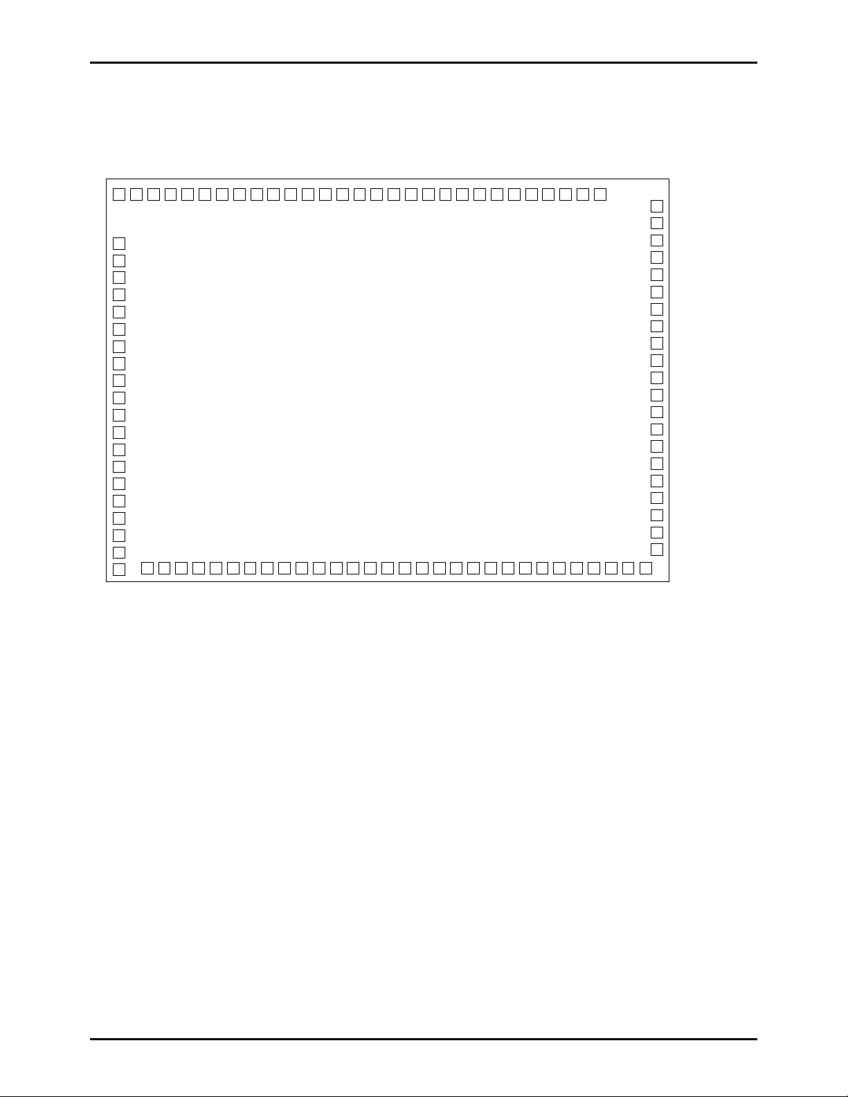
Pad Assignment
Chip size (X × Y) : 4.04mm
Thickness of chip : 480
Pad size : 105
Pad pitch : 110
81
82
83
84
85
86
87
88
89
90
91
92
93
94
95
96
97
98
99
100
× 3.21
m
µ
m × 105µm
µ
m
µ
mm
52 53 54 55 56 57 58 59 60 61 62 63 64 65 66 67 68 69 70 71 73 74 75 76 77 78 79 80 72
51
50
49
48
47
46
45
44
43
42
41
40
39
38
37
36
35
34
33
32
31
30 29 28 27 26 25 24 23 22 21 20 19 18 17 16 15 14 13 12 11 10 8 7 6 5 4 3 2 1 9
No.6703-3/21
Page 4

LC868920A
Pad name and Coord ina te s value
Pin No. Pad No. Name
1 1 S01 -1423 -1365 51 51 S51 1780 1352
2 2 S02 -1313 -1365 52 52 S52 1265 1364
3 3 S03 -1203 -1365 53 53 S53 1155 1364
4 4 S04 -1093 -1365 54 54 S54 1045 1364
5 5 S05 -983 -1365 55 55 S55 935 1364
6 6 S06 -873 -1365 56 56 S56 825 1364
7 7 S07 -763 -1365 57 57 S57 715 1364
8 8 S08 -653 -1365 58 58 S58 605 1364
9 9 S09 -543 -1365 59 59 S59 495 1364
10 10 S10 -433 -1365 60 60 S60 385 1364
11 11 S11 -323 -1365 61 61 S61 275 1364
12 12 S12 -213 -1365 62 62 S62 165 1364
13 13 S13 -103 -1365 63 63 S63 55 1364
14 14 S14 7 -1365 64 64 S64 -55 1364
15 15 S15 117 -1365 65 65 S65 -165 1364
16 16 S16 227 -1365 66 66 S66 -275 1364
17 17 S17 337 -1365 67 67 S67 -386 1364
18 18 S18 447 -1365 68 68 S68 --496 1364
19 19 S19 557 -1365 69 69 S69 -606 1364
20 20 S20 667 -1365 70 70 S70 -716 1364
21 21 S21 777 -1365 71 71 S71 -826 1364
22 22 S22 887 -1365 72 72 S72 -936 1364
23 23 S23 997 -1365 73 73 S73 -1046 1364
24 24 S24 1107 -1365 74 74 S74 -1156 1364
25 25 S25 1218 -1365 75 75 S75 -1266 1364
26 26 S26 1328 -1365 76 76 S76 -1376 1364
27 27 S27 1438 -1365 77 77 S77 -1486 1364
28 28 S28 1548 -1365 78 78 S78 -1596 1364
29 29 S29 1658 -1365 79 79 S79 -1706 1364
30 30 S30 1768 -1365 80 80 S80 -1816 1364
31 31 S31 1780 -849 81 81 V2 -1753 909
32 32 S32 1780 -739 82 82 V3 -1753 788
33 33 S33 1780 -629 83 83 V5 -1753 668
34 34 S34 1780 -519 84 84 VSS -1753 548
35 35 S35 1780 -408 85 85 DB0 -1753 428
36 36 S36 1780 -298 86 86 DB1 -1753 308
37 37 S37 1780 -188 87 87 DB2 -1753 188
38 38 S38 1780 -78 88 88 DB3 -1753 68
39 39 S39 1780 32 89 89 DB4 -1753 -52
40 40 S40 1780 142 90 90 DB5 -1753 -172
41 41 S41 1780 252 91 91 DB6 -1753 -292
42 42 S42 1780 362 92 92 DB7 -1753 -412
43 43 S43 1780 472 93 93 VDD -1753 -532
44 44 S44 1780 582 94 94 SCK -1753 -652
45 45 S45 1780 692 95 95
46 46 S46 1780 802 96 96
47 47 S47 1780 912 97 97
48 48 S48 1780 1022 98 98 RS -1753 -1132
49 49 S49 1780 1132 99 99 CL2 -1753 -1252
50 50 S50 1780 1242 100 100 M -1753 -1372
Coordinates Coordinates
Xµm Yµm
Pin No. Pad No. Name
CS
RD
WR
Xµm Yµm
-1753 -772
-1753 -892
-1753 -1012
Notes:
• When using LC868920A in the form of chip, connect the substrate of chip to VSS or leave it open.
No.6703-4/21
Page 5

LC868920A
System Block Diagra m
S80
V2
V3
V5
VDD
VSS
Latch for display data
START ADDRESS
LCD DRIVER
DUTY REGISTER
SCK
CL2
RS
RD
WR
CS
DB0
DB1
DB2
DB3
DB4
DB5
DB6
DB7
M
TIMING
GENERATOR
INSTRUCTION
REGISTER
ADDRESS REGISTER
ADDRESS REGISTER
LOWER CURSOR
HOTIZONTAL WORD
COUNT REGISTER
UPPER CURSOR
Terminal Form
A TYPE B TYPE
VDD
IN
VSS
Terminals: M, RS, RD, WR, CL2
IN
Terminals: SCK
C TYPE D TYPE
VDD
IN/OUT
Terminals: DB0 to DB7
DATA
OUTPUT
CONTROL
OUT
Terminals: S1 to S80
DOUT
UPPER AD DRESS
RAM
(128 0 BYTES)
LOWER ADDRESS
DIN
DOUT
S01
V5
V3
V2
VSS
No.6703-5/21
Page 6

LC868920A
Terminal Function Table
Terminal Pin No. Input/Output Function Description
VSS 84 - Negative power supply (-)
VDD 93 - Positive power supply (+)
DB0 - DB7 85 - 92 Input/Output Built-in Data bus
Terminals for sending/receiving data to/from the MPU
SCK 94 Input Clock for registers and disp lay RAM access
CS
RD
WR
RS 98 Input Register selection
CL2 99 Input LCD display signal (clock signal)
M 100 Input LCD display signal (synchronization signal)
V2
V3
V5
S1 - S80 1 - 80 Output LCD segment drive output terminal
95 Input Chip select terminal : Enable when CS=0
96 Input Read signal from LC868920A to LC868 364A
97 Input Write signal from LC868364A to LC868 920A
RS=1 : Instruction register
RS=0 : Data register
81
82
83
-
-
-
LCD power supply
No.6703-6/21
Page 7

LC868920A
1. Absolute Maximum Ratings at Ta=25°C, VSS=0V
Parameter Symbol Pins
Supply voltage VDDMAX VDD -0.3 - +7.0
LCD Input voltage VNMAX V2,V3,V5 VSS - +7.0
CS,RD,WR
CL2,M,SCK
(Input mode)
(Output mode)
,RS,
Maximum power
consumption
Operating
temperature
Storage
temperature
VI(1)
VI(2) DB0 to DB7
VO(1) S1 to S80 -0.3 - V5+0.3 Output voltage
VO(2) DB0 to DB7
Pdmax 200 mW
Topr -30 - 70
Tstg -55 - 125
Conditions Ratings
VDD[V] min. typ. max.
-0.3 - VDD+0.3 Input voltage
-0.3 VDD+0.3
-0.3 - VDD+0.3
*) The following condition has to be satisfied: V5 ≥ V3 ≥ V2 ≥ VSS
2. Recommended Operating Range at Ta=-30 to +70°C, VSS=0V
Parameter Symbol Pins
Operating
supply voltage
range
VDD VDD
VDD[V] min. typ. max.
FSCK ≤ 6MHz 3.3 6.5
FSCK ≤ 4MHz 2.7 6.5
Conditions Ratings
unit
V
C
°
unit
V
FSCK ≤ 3MHz 2.4 6.5
Supply voltage
range in Hold
mode
LCD supply
voltage range
High level input
voltage
Low level input
voltage
Input clock
frequency
VHD VDD
V5 V5
(Input mode)
CS,RD,WR
VIH(2) CL2,M,SCK
CS,RD,WR
VIL(3) CL2,M,SCK
FCL2 CL2 2.4 - 6.5 32 32.768 33 kHz
FSCK SCK
,RS
,RS
Keep RAM and
register data in
standby mode
VSS 6.5
2.0 6.5
4.5 - 6.5 0.75VDD VDD VIH(1) DB0 to DB7
2.4 - 4.5 0.75VDD VDD
4.5 - 6.5 0.75VDD VDD
2.4 - 4.5 0.75VDD VDD
4.5 - 6.5 0 0.25VDD VIL(1) DB0 to DB7 Input mode
2.4 - 4.5 0 0.25VDD
4.5 - 6.5 0 0.25VDD VIL(2)
2.4 - 4.5 0 0.25VDD
4.5 - 6.5 0 0.25VDD
2.4 - 4.5 0 0.25VDD
2.4 - 6.5 0.3 3
2.7 - 6.5 0.3 4
3.3 - 6.5 0.3 6
MHz
Note:
The specifications above concerning recommended operating conditions and electrical characteristics
assume the chip is in the QIP100E package. However, the LSI will be delivered in die form, not in a package.
The specifications will be very similar for the die, however, depending on factors such as the board on which
the chip is mounted, t he bonding pressure, and the moul ded plastic the characteristics will differ.
The ideal operating temperature for the above specifications is Ta= 25
C ± 2°C.
°
No.6703-7/21
Page 8

LC868920A
3. Electrical Characteristics at Ta=-30 to +70°C, VSS=0V
Parameter Symbol Pins
voltage
voltage
V5-Si drop voltage
(i:1 to 80)
VX-Si drop voltage
(X:2, 3) (i: 1 to 80)
VSS-Si drop voltage
(i:1 to 80)
Hysteresis voltage VHIS SCK 2.5 - 6.5 0.1VDD V
VOH(1) DB0 to DB7
VOL(1) DB0 to DB7
VD(1) S1 to S80
VD(2) S1 to S80
VD(3) S1 to S80
VDD[V] min. typ. max.
• Output mode
• IOH=-0.6mA
• Output mode
• IOH=-0.1mA
• Output mode
• IOL=+0.6mA
• Output mode
• IOL=+0.1mA
• -90µA for each
Si terminal
• V5-VSS=5V
• -15µA for each
Si terminal
• V5-VSS=5V
• -90µA for each
Si terminal
• V5-VSS=5V
• -15µA for each
Si terminal
• V5-VSS=5V
• +90µA for each
Si terminal
• V5-VSS=5V
• +15µA for each
Si terminal
• V5-VSS=5V
Conditions Ratings
4.5 - 6.5 2.4 VDD High level output
2.5 - 6.5 VDD-0.5 VDD
4.5 - 6.5 0 0.4 Low level output
2.5 - 6.5 0 0.4
4.5 - 6.5 630
2.5 - 6.5 120
4.5 - 6.5 200
2.5 - 6.5 120
4.5 - 6.5 -630
2.5 - 6.5 -120
unit
mV
4. Sample Current Dissipation Characterist ics at Ta=-30°C to +70°C, VSS=0V
The sample current dissipation characteristics shows the measurement result of Sanyo evaluation board.
The currents through the output transistors are ignored.
Parameter Symbol Pins
Current consumption
during normal operation
IDD(2)
IDD(3) • FCL2=32kHz
during READ/WRITE
operation to RAM or
registers
IDD(4) • FCL2=0Hz
during standby mode
VDD[V] min. typ. max.
• FSCK : stop
• Figure 1
• V2=V3=V5=VSS
• FCLK2=32kHz
• FSCK : stop
• Figure 4
• V5=5V, V3=3V,
V2=2V
• FSCK : 3MHz
• Figure 2
• V2=V3=V5=VSS
• FSCK : stop
• Figure 3
• V2=V3=V5=VSS
Conditions Ratings
4.5 - 6.5 7 15 IDD(1) • FCL2=32kHz
2.5 - 4.5 4 10
4.5 - 6.5
2.5 - 4.5
4.5 - 6.5 170 300 Current consumption
3.0 - 4.5 100 200
4.5 - 6.5 0.05 30 Current consumption
2.5 - 4.5 0.02 20
15 50
5 20
unit
V
A
µ
No.6703-8/21
Page 9

LC868920A
fCL2=32kHz
VDD
Open
A
VDD S1 S2 S80
SCK
CS
RD
WR
RS
M
LC868920A
CL2 VSS V2 V3 V5
DB0
DB1
DB2
DB3
DB4
DB5
DB6
DB7
VDD
Open
A
fSCK=3MHz
Open Open
Open
fCL2=32kHz
VDD S1 S2 S80
SCK
CS
RD
WR
RS
M
LC868920A
CL2 VSS V2 V3 V5
DB0
DB1
DB2
DB3
DB4
DB5
DB6
DB7
Figure 1 Current consumption measuring circuit Figure 2 Current consumption measuring circuit
during normal operation during READ/WRITE operation to
RAM or registers
Open
fCL2=0Hz
VDD
Open
A
VDD S1 S2 S80
SCK
CS
RD
WR
RS
M
LC868920A
CLK2 VSS V2 V3 V5
DB0
DB1
DB2
DB3
DB4
DB5
DB6
DB7
Open
Open
fCL2=32kHz
VDD
Open
A
VDD S1 S2 S80
SCK
CS
RD
WR
RS
M
LC868920A
CL2 VSS V2 V3 V5
2V 3V 5V
DB0
DB1
DB2
DB3
DB4
DB5
DB6
DB7
Figure 3 Current consumption measuring circuit Figure 4 Current consumption measuring circuit
during standby mode during LCD operation
Open
Open
No.6703-9/21
Page 10

AC Characteristics at Ta=-30 to +70°C, VSS=0V
(1) MPU Interface
1. Read/write clock
SCK
4
RD, WR
2. Read cycle
RD
CS
, RS
DB0 - DB7
3. Write cycle
WR
, RS
CS
DB0 - DB7
9
9
6
11
6
13
LC868920A
1
2
3
6
7
10
12
7
10
14
8
8
8
0.75VDD
0.25VDD
8
0.75VDD
0.25VDD
5
No.6703-10/21
Page 11

LC868920A
No Item Symbol
VDD MIN MAX
1 SCK clock cycle tsck SCK
Conditions Value
3.3 – 6.5 166 3340
2.7 – 6.5 249 3340
2.4 – 6.5 333 3340
2 SCK_H width pw1 SCK 2.4 – 6.5 0.45 0.55 tsck
3 SCK_L width tr1,tf1 SCK 2.4 – 6.5 0.45 0.55 tsck
RD, WR
set-up time
tRS
SCK, RD, WR
4.5 - 6.5 5 40 4
2.4 - 4.5 5 100
RD, WR
Hold time
tRH
SCK, RD, WR
4.5 - 6.5 5 40 5
2.4 - 4.5 5 100
6
RD, WR
pulse width
7 ENABLE cycle time
pw1
tcyc1
tcyc2
RD, WR
RD
WR
RD
2.4 – 6.5 3 6 tsck
2.4 – 6.5 12
2.4 – 6.5 12
4.5 - 6.5 20 8 Rising/Falling time tr1, tf1
2.4 - 4.5 40
9 Address set-up time
CS
, RS, RD
4.5 - 6.5 40 tAS1
2.4 - 4.5 40
tAS2
CS
, RS, WR
4.5 - 6.5 40
2.4 - 4.5 40
10 Address Hold time
11 Data delay time tDDR1
tAH1
tAH2
CS
, RS, RD
CS
, RS, WR
RD
, DB0 - DB7, CL=50pF
RD
, DB0 - DB7, CL=50pF
2.4 – 6.5 0.5
2.4 – 6.5 0.5
2.4 – 6.5 2 tsck
4.5 - 6.5 20 12 Data Hold time tDHR1
2.4 – 6.5 20
13 Data set-up time tDSW1
14 Data Hold time tDHW1
WR
, DB0 - DB7, CL=50pF
WR
, DB0 - DB7, CL=50pF
2.4 – 6.5 1.5 tsck
2.4 – 6.5 1 tsck
CL: Loading Capacity
unit
ns
ns
ns
tsck
ns
ns
ns
tsck
ns
No.6703-11/21
Page 12

LC868920A
(2) Display Control Timing at Ta=-30 to +70°C, VSS=0V
CL2
0.75VDD
2
0.25VDD
1
4 5
6
3
M
No Item Symbol
VDD MIN MAX
1 Clock cycle tCL2 CL2 2.4 - 6.5 30 31
2 Low level pulse width tWLCL2 CL2 2.4 - 6.5 13
3 High level pulse width tWHCL2 CL2 2.4 - 6.5 13
0.75VDD
0.25VDD
Conditions Value
4.5 - 6.5 20 4 Rising time tr CL2
2.4 - 4.5 50
4.5 - 6.5 20 5 Falling time tf CL2
2.4 - 4.5 50
4.5 - 6.5 60 6 M delay time tDM M
2.4 - 4.5 100
unit
s
µ
s
µ
s
µ
ns
ns
ns
No.6703-12/21
Page 13

LC868920A
(
Example circ uit for refe r en ce
1. 32 × 112 dots
External
Voltage up
converter
2. 32 × 192 dots
C32
C1
P40
VLCD
S32 S1
2KOUT)
LC868364A LC868920A
LCD Panel (32 × 112 dots)
P41(CL2)
P42(LCDP2)
P43(M)
P00
P01
P02
P03
P04
P05
P06
P07
P46(RD)
P47(WR)
P44
P45
VDD
V2
V3
V5
VSS
LCD Panel (32 × 192 dots)
S80 S1
CL2
SCK
M
DB0
DB1
DB2
DB3
DB4
DB5
DB6
DB7
RD
WR
CS
RS
VDD
V2
V3
V5
VSS
External
Voltage up
converter
C32
C1
P40(2KOUT)
VLCD
P0
P46(RD)
S32 S1
S80 S1 S80 S1
LC868364A LC868920A LC868920A
P47(WR)
P44
P45
P41(CL2)
P42(LCDP2)
P43(M)
LCD power
VDD
VSS
DB
RD
WR
CS
RS
CL2
SCK M LCD power
VDD
VSS
DB
RD
WR
CS
RS
CL2
SCK M LCD power
VDD
VSS
No.6703-13/21
Page 14

LC868920A
!
Evaluation Sample (ES)
Shipping Form: LC868920A: chip, Evaluation sample: QIP100E (shown below) or chip
If you use the ES in the package to design and fabricate an evaluation board, refer to the following pin assignment.
Terminal Assignment
S80
S79
S78
S77
S76
S75
S74
S73
S72
S71
S70
S69
S68
S67
S66
S65
S64
S63
S62
S61
S60
S59
S58
S57
S56
S55
S54
S53
S52
S51
V2
V3
V5
VSS
DB0
DB1
DB2
DB3
DB4
DB5
DB6
DB7
VDD
SCK
CS
RD
WR
RS
CL2
M
8079787776757473727170696867666564636261605958575655545352
81
82
83
84
85
86
87
88
89
90
91
92
93
94
95
96
97
98
99
100
1 2 3 4 5 6 7 8 9
10
11
12
13
14
15
16
17
18
19
20
21
22
23
24
25
26
27
28
29
51
50
49
48
47
46
45
44
43
42
41
40
39
38
37
36
35
34
33
32
31
30
S50
S49
S48
S47
S46
S45
S44
S43
S42
S41
S40
S39
S38
S37
S36
S35
S34
S33
S32
S31
S1S2S3S4S5S6S7S8S9
S10
S11
S12
S13
S14
S15
S16
S17
S18
S19
S20
S21
S22
S23
S24
S25
S26
S27
S28
S29
S30
Package Dimension
(unit : mm)
3151
SANYO : QIP-100E
(FLP100)
No.6703-14/21
Page 15

LC868920A
Functions
1. Interface control
The interface control block consists of the instruction register and the timing generator.
(Note) When accessing to registers or the display RAM of LC868920A, the system clock of LC868364A has to be either
CF oscillation or RC oscillation. It will cause the irregular operation if the crystal oscillation is used in
LC868364A when reading/writing data from/to LC868920A.
The STX instruction of LC868364A should be used to write data to LC868920A. The LDX instruction of
LC868364A should be used to read data from LC868920A.
(1) Instruction register (4-bit data)
- When RS = '1', the lower 4-bits data of the eight bit data bus (DB0-DB7) is sent to this register.
- The following conditions have to be set to write data to the instruction register.
= '0' : Enable the chip select.
1.
CS
= '0' : Writing mode from LC868364A to LC868920A
2.
WR
3. RS = '1' : Select the instruction register.
4. Feed clock to SCK.
- The value of the instruction registers serves as the address of 7 kinds of data registers.
The instruction register holds the data until the instruction code is rewritten. A list of instruction codes is shown below.
Instruction code
DB3 DB2 DB1 DB0
0 0 1 0 Select the horizontal word count register
0 0 1 1 Select the duty register
1 0 0 0 Sel ect the start address register
1 0 1 0 Select the lower cursor address register
1 0 1 1 Select the upper cursor address register
1 1 1 0 Set the display data writing mode
1 1 1 1 Set the display data reading mode
Description
Notes:
Don’t write to the Test Register.
The Test Register can be specified by writing ‘00H’ to the Instruction Register. However, setting any bits in this register
will cause malfunction since this register is only used for testing.
(2) Writing to each data register
- The following indicates how to write data to the registers or the display RAM specified by the instruction register setting.
- The following conditions should be set to write data to each register or the display RAM.
= '0' : Enable the chip select
1.
CS
2.
= '0' : Writing mode from LC868364A.to LC868920A
WR
3. RS = '0' : Select writing data
4. Feed clock to SCK
- The data output from LC868364A through the 8 bits data bus (DB0 - DB7) is written to the register specified by the
instruction register. (Data can not be written without a SCK clock signal.)
- By selecting the display data writing mode with the instruction register and setting the condition shown above, the output
data from LC868364A through the data bus (DB0 - DB7) is written to the display RAM address specified by the cursor
address. After the completion of writing, the cursor address is automatically decremeted by 1. Therefore, the data can
be written contiguously to the display RAM.
No.6703-15/21
Page 16

LC868920A
(3) Reading display RAM
- Refer to "Section 2 Display control registers and display RAM (8)" about how to output the display RAM data to the data
bus (DB0 - DB7).
- The following conditions are necessary to be set to read display RAM data.
= '0' : Enable the chip select
1.
CS
= '0' : Reading mode from LC868920A to LC868364A
2.
RD
3. RS = '0' : Select the display RAM
4. Feed clock to SCK.
- Each time data is read from the display RAM, the address of the display RAM (cursor address) is automatically
decremented by 1.
(4) Timing generator
- The interface control block and the display are controlled by the timing signals and control signals generated in this circuit.
The control signals and timing signals are used to transfer the data output from terminals DB0 - DB7 to the internal
registers and to transfer data between terminals DB0 - DB7 and the display RAM. This circuit also produces the data
input/output control signals and read/write timing signals.
2. Display control registers and display RAM
- The display is controlled by writing data to the instruction register and 7 internal data registers.
(1) LCD drive frequency
- DP indicates the number of clocks which is necessary to display 1 word (16 dots). DP is fixed to '2' in
LC868920A.
- LC868920A is a segm ent driver to exp and the L CD dis play capability for LC86 8364A. The common signal is
output from LC868364A. Therefore, the number of dots to display a line may vary between the internal driver
in microcontr oller and the segmen t driver for expansion. Even if the num ber of display dots is different, the
LCD driver frequency has to be the same on each side.
(Example 1) When selecting 32 COM × 32SEG in LC868364A
The number of dots per line in microcontroller : 32 dots
The number of dots per line in LC868920A : 80 dots
The time required to display a line is the same for both the microcontroller and LC868920A by setting as
follows.
LC868364A : HP = 5 32 × 5 (Hp) = 160
LC868920A : Dp = 2 80 × 2 (Dp) = 160
32
C1
|
C32
S32 - S1 S80 - S1
LCD Panel
32
80
LC868364A LC868920A
No.6703-16/21
Page 17

LC868920A
(Example 2) When selectin g 16COM in LC868364A
The number of dots per line in LC868920A : 80 dots
80 × 2 (DP) = 160
It is necessary to set as follows to have the s ame t ime re quired to display a line in LC86836 4A as in
LC868920A.
32 × 5 (Hp) = 160
(Note) If 16COM is selected in LC868364A and LC868920A is used to expand segments, S1 to S32 segments
can only be used in LC868364A and segment s S3 3 to S48 can not be used. HP = 5 should be set to
LC868364A by program.
16
C1
|
C16
LCD Panel
32
80
(Note)
S33 to S48 can not be used.
S32 - S1 S80 - S1
LC868364A LC868920A
(2) Horizontal word count register
Register
Instruction register 1 0 1 0 0 0 0 0 0 1 0
Horizontal
word
count register
RD WR
1 0 0 - - - - Dn-1
RS DB7 DB6 DB5 DB4 DB3 DB2 DB1 DB0
- This register sets the number of horizontal words.
- Dn indicates the number of words in horizontal direction.
- The total number of horizontal dots on the LCD panel (n) is given by the following formula.
n = 8 × (Dn ×2) (n
≤
80)
- 1 to 5 ( in decimal) can be set as Dn.
- The relation between the total number of horizontal dots (n), the number of horizontal words (Dn) and register settings is
shown below.
Total number of horizontal dots (n) Dn DB2 DB1 DB0
16 1 0 0 0
32 2 0 0 1
48 3 0 1 0
64 4 0 1 1
80 5 1 0 0
(3) Duty register
Register
Instruction register 1 0 1 0 0 0 0 0 0 1 1
Divider ratio register 1 0 0 0 0 Nx-1
RD WR
RS DB7 DB6 DB5 DB4 DB3 DB2 DB1 DB0
- This register sets the divider ratio (Nx). (Display duty = 1/Nx)
- Nx represents the divider ratio of display and 1/Nx indicates a display duty.
- 2 to 32 (in decimal) can be set as Nx.
No.6703-17/21
Page 18

(4) Start address register
LC868920A
Register
Instruction register 1 0 1 0 0 0 0 1 0 0 0
Start address register 1 0 0 0 Start Address (STAD)
RD WR
RS DB7 DB6 DB5 DB4 DB3 DB2 DB1 DB0
- This register sets the value of display start line address.
- The display start line address shows the RAM line address of the data to be displayed in the top line on the LCD panel.
- The start address counter is a 7-bit down-counter with a preset function.
- The start address (STAD) is set to the start address counter as an initial value.
- The start address counter is decremented by 1 each time the display of a line in horizontal direction is completed on the
screen.
- The start address counter takes the value 7FH on the next decrement after 0.
(5) Lower cursor address register
Register
Instruction register 1 0 1 0 0 0 0 1 0 1 0
Cursor address counter
(lower byte)
RD WR
1 0 0 0 0 0 0 Lower cursor address (CAL)
RS DB7 DB6 DB5 DB4 DB3 DB2 DB1 DB0
- Set the lower address used to read/write data from/to the display RAM in this register.
- The lower cursor address counter is a 4-bit down-counter with a preset function.
- The lower cursor address (CAL) is set to the counter as an initial value.
- This counter is decremented by 1 each time the RAM is accessed.
- If RAM is accessed when the value of this counter is "0", then Dn-1 is automatically set.
- 0 to 9 (in decimal) can be set as a lower cursor address.
(6) Upper cursor address register
Register
Instruction register 1 0 1 0 0 0 0 1 0 1 1
Cursor address counter
(upper byte)
RD WR
1 0 0 0 Upper cursor address (CAH)
RS DB7 DB6 DB5 DB4 DB3 DB2 DB1 DB0
- Set the upper addresses used to read/write data from/to the display RAM in this register.
- The upper cursor address counter is a 7-bit down-counter with a preset function.
- This counter is decremented by 1 each time the lower cursor address counter generates the underflow.
- The cursor address is written to the cursor address counter by setting data to the lower and upper cursor address registers.
- The cursor address indicates the RAM address to access display data. The data of the address specified by the cursor
address is read /written from/to the display RAM.
- The cursor address consists of the 4-bit lower address and 7-bit upper address.
(7) Display RAM
Writing data to Display RAM
a
.)
Register
Instruction register 1 0 1 0 0 0 0 1 1 1 0
RAM 1 0 0 MSB Display pattern data LSB
RD WR
RS DB7 DB6 DB5 DB4 DB3 DB2 DB1 DB0
- Select the display data writing mode by setting "0EH" to the instruction register. Then set RS = 0 and write 8-bit data to
the display RAM.
The display pattern data is written to the RAM address specified by the cursor address. After writing data to RAM, the
cursor address counter is automatically decremented by 1.
No.6703-18/21
Page 19

b.) Reading data from display RAM
D
LC868920A
Register
RD WR
RS DB7 DB6 DB5 DB4 DB3 DB2 DB1 DB0
Instruction register 1 0 1 0 0 0 0 1 1 1 1
RAM 0 1 0 MSB Display pattern data LSB
- Select the display data reading mode by setting ‘0FH’ to the instruction register. Then set RS=0 and select the display
RAM.
- The procedure of reading RAM data is as follows:
(1) The RAM data of the address specified by the cursor address is output to DB0 to DB7 terminals by setting as
shown above.
(2) The cursor address counter is decremented by 1.
The following figure indicates the procedure of reading RAM data.
Conditions
• Instruction register (IR) = OFH
• RS=0
=0
•
RD
(2)
-1
DB0
DB1
D0
D1
RAM data
A0 to A10
Cursor
address
counter
11 bits
DB7
D7
(1) RAM DATA is output to DB terminals
(1) Output control (OE)
e.x.) Writing (reading) data to (from) display RAM
• Lower cursor address (CAL) =03H
• Upper cursor address (CAH) =02H
• The number or horizontal bytes (Dn)=05H
• Internal RAM capacity =1280 bytes
00H 01H 02H 03H 04H
10H 11H 12H 13H 14H
20H 21H 22H 23H 24H
30H 31H 32H 33H 34H
7F0H 7F1H 7F2H 7F3H 7F4H
If the writing operation is executed when the value of the
lower cursor address counter is ‘0’, the upper cursor address
counter is decremented by 1 after the completion of writing.
Then (Dn-1) is set to the lower cursor address counter.
Specified by the cursor address
First, data is written to this RAM address.
ecremented by 1 after the completion of writing.
If the writing operation is executed when the cursor address is ‘00H’,
then "7FH" is set to the upper cursor address counter after the
completion of writing.
(Dn-1) is set to the lower cursor address counter.
Notes:
Don’t write to the Test Register.
The Test Register can be specified by writing ‘00H’ to the Instruction Register. However, setting any bits in this register
will cause malfunction since this register is only used for testing.
No.6703-19/21
Page 20

LC868920A
3. LCD driver
- 4 levels of the LCD driving voltage (V5, V3, V2, and VSS) are externally supplied. The LCD driving voltage level to be
output to the segment drivers S1 to S80 vary according to the contents of the display data latch and the synchronous signal (M
signal).
- The 8-bit data output from the display RAM is input to the display data latch. The input 8-bit data is latched in the display
data latch for the number of bytes specified by the horizontal byte count register. This operation is repeated for the number
of times that is determined by the divide ratio number.
- The LCD display voltage has to be supplied to V2, V3 and V5 terminals after all data is set to LCD display data registers and
the display RAM. After power is on, if the LCD display voltage is supplied to V2, V3, and V5 terminals without setting
data to the internal registers and the display RAM, uncertain display is appeared on LCD panel. Thus, supply the VSS level
to V2, V3 and V5 terminals until all data required to display is set to data registers and the display RAM.
(Actually, the LCD display voltage is supplied to this circuit from LC868364A microcontroller. Therefore, turn OFF the
LCD display in LC868364A until data is set to the internal registers and the display RAM in LC868920A)
Display examples
(1) Display mode control register=01H (LCD: ON)
The total number of horizontal dots=80 (Dn=5)
Divider ratio (Nx)=32
Start address register=1FH
S80 - - - - S73 S72 - - - -S65 S64- - - -S57 S56- - - -S49 S48- - - -S41 S40- - - -S33 S32- - - - -S25 S24- - - -S17 S16- - - -S9 S8 - - - - -S1
↓ ↓ ↓ ↓ ↓ ↓ ↓ ↓ ↓ ↓ ↓ ↓ ↓ ↓ ↓ ↓ ↓ ↓ ↓
↓
MSB (1F0H)
C1 →
C2 →
C3 →
C28→
C29→
C30→
C31→
C32→
LSB
MSB (1E0H) LSB MSB (1E1H) LSB MSB (1E2H) LSB MSB (1E3H) LSB MSB (1E4H) LSB MSB (1E5H) LSB MSB (1E6H) LSB MSB (1E7H) LSB MSB (1E8H) LSB MSB (1E9 H) LSB
MSB (1D0H) LSB MSB (1D1H) LSB MSB (1D2H) LSB MSB (1D3 H) LSB MSB (1D4H) LSB MSB (1D5H) LSB MSB (1D6H) LSB MSB (1D7H) LSB MSB (1D8H) LSB MSB (1D9H) LSB
- - - -
MSB (040H) LSB MSB (041H) LSB MSB (042H) LSB MSB (043H) LSB MSB (044H) LSB MSB (045H) LSB MSB (046H) LSB MSB (047H) LSB MSB (048H) LSB MSB (0 49H) LSB
MSB (030H) LSB MSB (031H) LSB MSB (032H) LSB MSB (033H) LSB MSB (034H) LSB MSB (035H) LSB MSB (036H) LSB MSB (037H) LSB MSB (038H) LSB MSB (039H) LSB
MSB (020H) LSB MSB (021H) LSB MSB (022H) LSB MSB (023H) LSB MSB (024H) LSB MSB (025H) LSB MSB (026H) LSB MSB (027H) LSB MSB (028H) LSB MSB (029H) LSB
MSB (010H) LSB MSB (011H) LSB MSB (012H) LSB MSB (013H) LSB MSB (014H) LSB MSB (015H) LSB MSB (016H) LSB MSB (017H) LSB MSB (018H) LSB MSB (019H) LSB
MSB (000H) LSB MSB (001H) LSB MSB (002H) LSB MSB (003H) LSB MSB (004H) LSB MSB (005H) LSB MSB (006H) LSB MSB (007H) LSB MSB (008H) LSB MSB (009H) LSB
MSB (1F1H)
LSB
MSB (1F2H)
LSB
MSB (1F3H)
LSB
MSB (1F4H)
LSB
MSB (1F5H)
LSB
MSB (1F6H)
LSB
MSB (1F7H)
LSB
MSB (1F8H)
LSB
MSB (1F9H)
LSB
(2) Display mode control register=01H (LCD: ON)
The total number of horizontal dots=80 (Dn=5)
Divider ratio (Nx)=32
Start address register=1EH
S80 - - - S73 S72 - - - S65 S64 - - - S57 S56 - - - S49 S48 - - - S41 S40 - - - S33 S32 - - - S25 S24 - - - S17 S16 - - - - S9 S8 - - - - S1
↓ ↓ ↓ ↓ ↓ ↓ ↓ ↓ ↓ ↓ ↓ ↓ ↓ ↓ ↓ ↓ ↓ ↓ ↓
↓
MSB (1E0H) LSB MSB (1E1H) LSB MSB (1E2H) LSB MSB (1E3H) LSB MSB (1E4H) LSB MSB (1E5H) LSB MSB (1E6H) LSB MSB (1E7H) LSB MSB (1E8H) LSB MSB (1E9H) LSB
C1 →
MSB (1D0H) LSB MSB (1D1H) LSB MSB (1D2H) LSB MSB (1D3H) LSB MSB (1D4 H) LSB MSB (1D5H) LSB MSB (1D6H ) LSB MSB (1D7H) LSB MSB (1D8H) LSB MSB (1D9H) LSB
C2 →
MSB (1C0H) LSB MSB (1C1H) LSB MSB (1C2H) LSB MSB (1C3H) LSB MSB (1C4H) LSB MSB (1C5H) LSB MSB (1C6H) LSB MSB (1C7H) LSB MSB (1C8H) LSB MSB (1C9H) LSB
C3 →
- - - -
C28→
C29→
C30→
C31→
C32→
MSB (030H) LSB MSB (041H) LSB MSB (042H) LSB MSB (043H) LSB MSB (044H) LSB MSB (045H) LSB MSB (046H) LSB MSB (047H) LSB MSB (048H) LSB MSB (049H) LSB
MSB (020H) LSB MSB (031H) LSB MSB (032H) LSB MSB (033H) LSB MSB (034H) LSB MSB (035H) LSB MSB (036H) LSB MSB (037H) LSB MSB (038H) LSB MSB (039H) LSB
MSB (010H) LSB MSB (021H) LSB MSB (022H) LSB MSB (023H) LSB MSB (024H) LSB MSB (025H) LSB MSB (026H) LSB MSB (027H) LSB MSB (028H) LSB MSB (029H) LSB
MSB (000H) LSB MSB (011H) LSB MSB (012H) LSB MSB (013H) LSB MSB (014H) LSB MSB (015H) LSB MSB (016H) LSB MSB (017H) LSB MSB (018H) LSB MSB (019H) LSB
MSB (7F0H) LSB MSB (7F1H) LSB MSB (7F2H) LSB MSB (7F3H) LSB MSB (7F4H) LSB MSB (7F5H) LSB MSB (7F6H) LSB MSB (7F7H) LSB MSB (7F8H) LSB MSB (7F9H) LSB
No.6703-20/21
Page 21

LC868920A
(3) Display mode control register=01H (LCD: ON)
The total number of horizontal dots=80 (Dn=5)
Divider ratio (Nx)=16
Start address register=0FH
S80 - - - S73 S72 - - - S65 S64 - - - S57 S56 - - - S49 S48 - - - S41 S40 - - - S33 S32 - - - S25 S24 - - - S17 S16 - - - - S9 S8 - - - - - S1
↓ ↓ ↓ ↓ ↓ ↓ ↓ ↓ ↓ ↓ ↓ ↓ ↓ ↓ ↓ ↓ ↓ ↓ ↓
↓
MSB (0F0H) LSB MSB (0F1H) LSB MSB (0F2H) LSB MSB (0F3H) LSB MSB (0F4H) LSB MSB (0F5H) LSB MSB (0F6H) LSB MSB (0F7H) LSB MSB (0F8H) LSB MSB (0F9H) LSB
C1 →
MSB (0E0H) LSB MSB (0E1H) LSB MSB (0E2H) LSB MSB (0E3H) LSB MSB (0E4H) LSB MSB (0E5H) LSB MSB (0E6H) LSB MSB (0E7H) LSB MSB (0E8H) LSB MSB (0E9H) LSB
C2 →
MSB (0D0H) LSB MSB (0D1H) LSB MSB (0D2H) L SB MSB (0D3H) LSB MSB (0D4H) LSB MSB (0D5H) LSB MSB (0D6H ) LSB MSB (0D7H) LSB MSB (0D8H) LSB MSB (0D9H) LSB
C3 →
- - - -
C12→
C13→
C14→
C15→
C16→
MSB (040H) LSB MSB (041H) LSB MSB (042H) LSB MSB (043H) LSB MSB (044H) LSB MSB (045H) LSB MSB (046H) LSB MSB (047H) LSB MSB (048H) LSB MSB (049H) LSB
MSB (030H) LSB MSB (031H) LSB MSB (032H) LSB MSB (033H) LSB MSB (034H) LSB MSB (035H) LSB MSB (036H) LSB MSB (037H) LSB MSB (038H) LSB MSB (039H) LSB
MSB (020H) LSB MSB (021H) LSB MSB (022H) LSB MSB (023H) LSB MSB (024H) LSB MSB (025H) LSB MSB (026H) LSB MSB (027H) LSB MSB (028H) LSB MSB (029H) LSB
MSB (010H) LSB MSB (011H) LSB MSB (012H) LSB MSB (013H) LSB MSB (014H) LSB MSB (015H) LSB MSB (016H) LSB MSB (017H) LSB MSB (018H) LSB MSB (019H) LSB
MSB (000H) LSB MSB (001H) LSB MSB (002H) LSB MSB (003H) LSB MSB (004H) LSB MSB (005H) LSB MSB (006H) LSB MSB (007H) LSB MSB (008H) LSB MSB (009H) LSB
(4) Display mode control register=01H (LCD: ON)
The total number of horizontal dots=64 (Dn=4)
Divider ratio (Nx)=16
Start address register=1FH
S64 - - - S57 S56 - - - S49 S48 - - - S41 S40 - - - S33 S32 - - - S25 S24 - - - S17 S16 - - - - S9 S8 - - - - S1
↓ ↓ ↓ ↓ ↓ ↓ ↓ ↓ ↓ ↓ ↓ ↓ ↓ ↓ ↓
↓
MSB (1F0H) LSB MSB (1F1H) LSB MSB (1F2H) LSB MSB (1F3H) LSB MSB (1F4H) LSB MSB (1F5H) LSB MSB (1F6H) LSB MSB (1F7H) LSB
C1 →
MSB (1E0H) LSB MSB (1E1H) LSB MSB (1E2H) LSB MSB (1E3H) LSB MSB (1E4H) LSB MSB (1E5H) LSB MSB (1E6H) LSB MSB (1E7H) LSB
C2 →
MSB (1D0H) LSB MSB (1D1H) LSB MSB (1D2H) LSB MSB (1D3H) LSB MSB (1D4H) LSB MSB (1D5H) LSB MSB (1D6H) LSB MSB (1D7H) LSB
C3 →
- - - -
C12→
C13→
C14→
C15→
C16→
MSB (140H) LSB MSB (141H) LSB MSB (142H) LSB MSB (143H) LSB MSB (144H) LSB MSB (145H) LSB MSB (146H) LSB MSB (147H) LSB
MSB (130H) LSB MSB (131H) LSB MSB (132H) LSB MSB (133H) LSB MSB (134H) LSB MSB (135H) LSB MSB (136H) LSB MSB (137H) LSB
MSB (120H) LSB MSB (121H) LSB MSB (122H) LSB MSB (123H) LSB MSB (124H) LSB MSB (125H) LSB MSB (126H) LSB MSB (127H) LSB
MSB (110H) LSB MSB (111H) LSB MSB (112H) LSB MSB (113H) LSB MSB (114H) LSB MSB (115H) LSB MSB (116H) LSB MSB (117H) LSB
MSB (100H) LSB MSB (101H) LSB MSB (102H) LSB MSB (103H) LSB MSB (104H) LSB MSB (105H) LSB MSB (106H) LSB MSB (107H) LSB
No.6703-21/21
PS
 Loading...