

Page 1
Ordering number: EN 5650
LC865020B/16B/12B/08B
CMOS LSI
LC865020B/16B/12B/08B
8-Bit Single-Chip Microcontroller
Overview
The LC865020B/16B/12B/08B microcontrollers are 8-bit
single-chip microcontrollers with the following on-chip
functional blocks :
• CPU : Operable at a minimum bus cycle time of 0.5 µs
(microsecond)
• On-chip ROM capacity : Up to 20K bytes
• On-chip RAM capacity : 384 bytes
(LC865020B/16B/12B/08B)
• 16-bit timer/counter (or two 8-bit timers)
• 16-bit timer/PWM (or two 8-bit timers)
• 8-channel × 8-bit A/D converter
• Two 8-bit synchronous serial-interface circuits
• 13-source 10-vectored interrupt system
All of the functions above are fabricated on a single chip.
Features
(1) Read-Only Memory (ROM) :
LC865020B 20480 × 8 bits
LC865016B 16384 × 8 bits
LC865012B 12288 × 8 bits
LC865008B 8192 × 8 bits
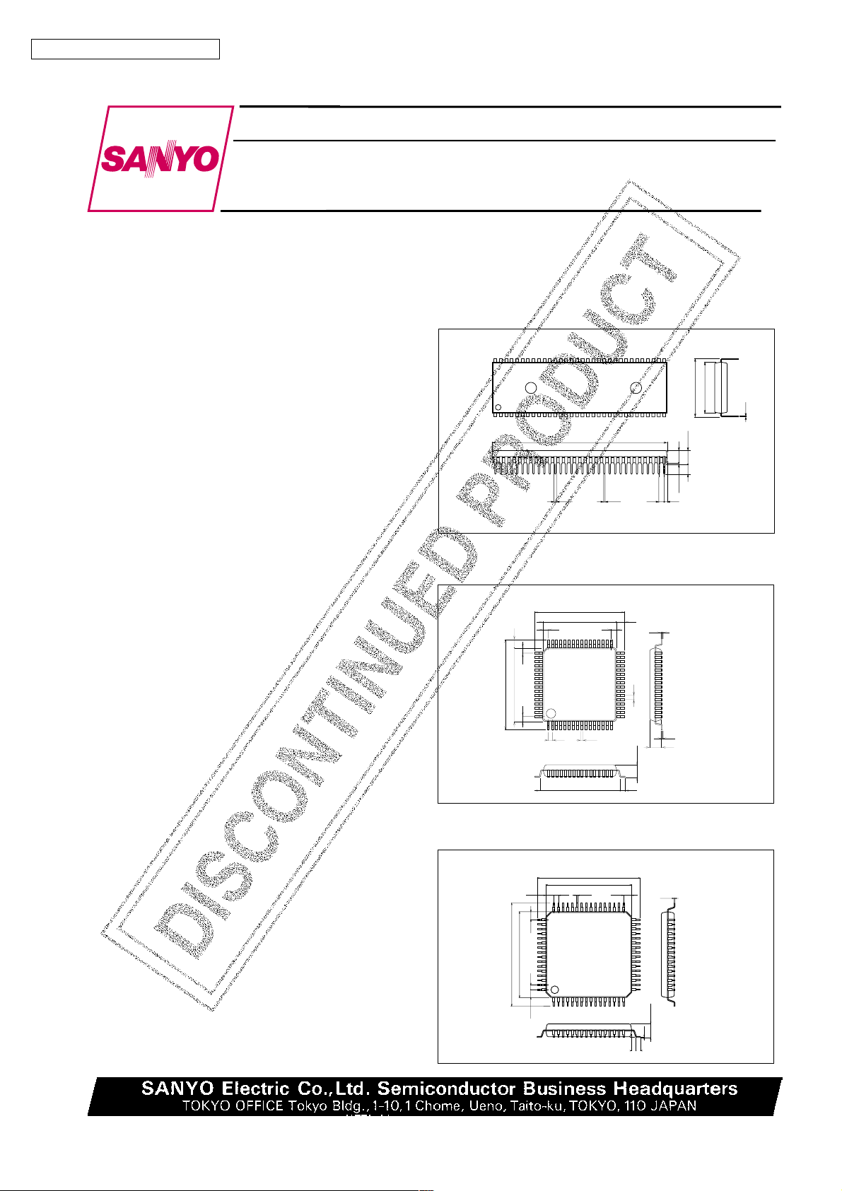
Package Dimensions
unit : mm
3071-DIP64S
[LC865020B/16B/12B/08B]
57.2
0.95 0.48 1.78 1.01
unit : mm
3159-QFP64E
[LC865020B/16B/12B/08B]
17.2
14.0
17.2
1.6
14.0
1.0
1.0
1.0
48
49
64
1
0.8
0.35
1.0
33
32
17
16
3364
321
4.00.51min
SANYO : DIP64S
1.6
0.15
0.8
0.1
2.7
3.0max
5.0max
3.2
19.5
16.8
0.25
(2) Random Access Memory (RAM) :
LC865020B/16B/12B/08B 384 × 8 bits
SANYO Electric Co., Ltd. Semiconductor LSI Div. Microcomputer Development Dep.
unit : mm
3190-SQFP64
1.25 0.5 1.250.18
10.0
12.0
15.6
0.8
SANYO : QFP64E
[LC865020B/16B/12B/08B]
12.0
10.0
0.15
48
49
1.25
0.5
64
116
1.25
33
32
17
1.7max
0.1
0.5
0.5
SANYO : SQFP64
O3097HA (II)
No. 5650-1/21
Page 2
LC865020B/16B/12B/08B
(3) Bus cycle time / Instruction cycle time
The LC865020B/16B/12B/08B microcontrollers are constructed to read ROM twice within one instruction cycle. This results
in 1.7 times better performance within the same instruction cycle compared to our 4-bit microcontrollers (the LC66000 series).
Bus cycle time indicates the speed to read ROM.
Bus cycle time Cycle time System clock oscillation Oscillation frequency Supply voltage
0.5 µs1 µs Ceramic resonator 12 MHz 4.5 to 6.0V
2 µs4 µs Ceramic resonator 3 MHz 2.7 to 6.0V
7.5 µs 15 µs RC oscillator 800 kHz 2.7 to 6.0V
183 µs 366 µs Crystal oscillator 32.768 kHz 2.7 to 6.0V
(4) Ports
- Input/output ports : 6 ports (42 pins)
Input/output port programmable in nibble units : 1 port (8 pins)
(However, when N-channel open-drain output is selected, bit-unit input is possible.)
Input/output port each bit programmable : 5 ports (34 pins)
Include 15 V withstand N-channel open drain output port : 3 ports (18 pins)
- Input ports : 2 ports (13 pins)
(5) A/D converter
- 8-channel × 8-bit A/D converter
(6) Serial-interface
- Two 8-bit serial-interface circuits
LSB first / MSB first functions switchable
- Internal 8-bit band-rate generator in common with two serial-interface circuits
(7) Timer
- Timer 0
16-bit timer/counter
2-bit prescaler + 8-bit programmable prescaler
Mode 0 : Two 8-bit timers with programmable prescaler
Mode 1 : 8-bit timer with programmable prescaler + 8-bit counter
Mode 2 : 16-bit timer with programmable prescaler
Mode 3 : 16-bit counter
The resolution of Timer is fixed to tCYC. (tCYC : cycle time)
- Timer 1
16-bit timer/PWM
Mode 0 : Two 8-bit timers
Mode 1 : 8-bit timer + 8-bit PWM
Mode 2 : 16-bit timer
Mode 3 : Variable-bit PWM (9 to 16 bits)
In Mode 0 and Mode1, the resolution of Timer and PWM is fixed to tCYC.
In Mode 2 and Mode 3, the resolution of Timer and PWM can be programmed to be tCYC or 1/2 tCYC
- Base timer
Every 500 ms overflow system for clock applications (using 32.768 kHz crystal oscillator for Base timer clock)
Every 976 µs, 3.9 ms, 15.6 ms, 62.5 ms overflow system (using 32.768 kHz crystal oscillator for Base timer clock)
- Base timer clock selectable
32.768 kHz crystal oscillator, system clock, and programmable prescaler output of Timer 0
No. 5650-2/21
Page 3
LC865020B/16B/12B/08B
(8) Buzzer output
- The buzzer sound frequency is selectable ; 4 kHz, 2 kHz (using 32.768 kHz crystal oscillator for base timer clock)
(9) Remote-controlled receiver circuit (shares P73/INT3/T0IN pin)
- Noise rejection function
- Polarity switching
(10) Watchdog timer
- RC external watchdog timer
- Watchdog timer operation can be selected : Interrupt/reset
(11) Interrupt system
- 13-source 10-vectored interrupts :
1. External interrupt INT0 (including watchdog timer)
2. External interrupt INT1
3. External interrupt INT2, Timer/counter T0L (lower 8 bits)
4. External interrupt INT3, base timer
5. Timer/counter T0H (upper 8-bits)
6. Timer T1L, timer T1H
7. Serial-interface SIO0
8. Serial-interface SIO1
9. A/D converter
10. Port 0
- Built-in interrupt priority control register
Microcontroller supports 3 levels of multiple interrupt; low level, high level, and highest level. For the 11 interrupt requests
from INT2 through Port 0, high/low level interrupt priority can be specified using the priority control register. Also, for
INT0 and INT1, highest/low level interrupt priority can be specified.
(12) Real-time service operation
Synchronizing with the interrupt request signals, the real-time service starts a 4-byte data transfer between which special
function registers within 1-instruction cycle after the request signal occurs, and then completes its operation within
5-instruction cycles. This operation is performed in parallel with CPU operation.
(13) Subroutine stack
- 128 levels (Max.) : The stack is located in RAM.
(14) Multiplication and division
16 bits × 8 bits (7-instruction cycles)
16 bits / 8 bits (7-instruction cycles)
(15) 3 oscillation circuits
- On-chip RC oscillator circuit for the system clock
- On-chip CF oscillator circuit for the system clock
- On-chip crystal oscillator circuit for the system clock and the time-base clock
XT1 pin can be used as P74.
No. 5650-3/21
Page 4
LC865020B/16B/12B/08B
(16) Standby function
- HALT mode
HALT mode is used to reduce power dissipation. In this mode, program execution is stopped. This mode can be released by
an interrupt request signal or initial system reset request signal.
- HOLD mode
The HOLD mode is used to stop all oscillators RC (internal), CR and Crystal. This mode can be released by the following
operations
• Set Low level to Reset pin (RES).
• Set predefined level to P70/INT0, P71/INT1 pins (programmable).
• Set Low level to Port 0 pin/pins (programmable).
(17) Factory shipment
• DIP64S , QFP64E , SQFP64 delivery form
(18) Development support tools
Evaluation (EVA) chip : LC866098
EPROM version : LC86E5032
One time ROM version : LC86P5032
Emulator : EVA-86000 + ECB866600 (Evaluation chip board)
+ POD865000 (POD for DIP64S)
+ POD865010 (POD for QFP64E)
No. 5650-4/21
Page 5
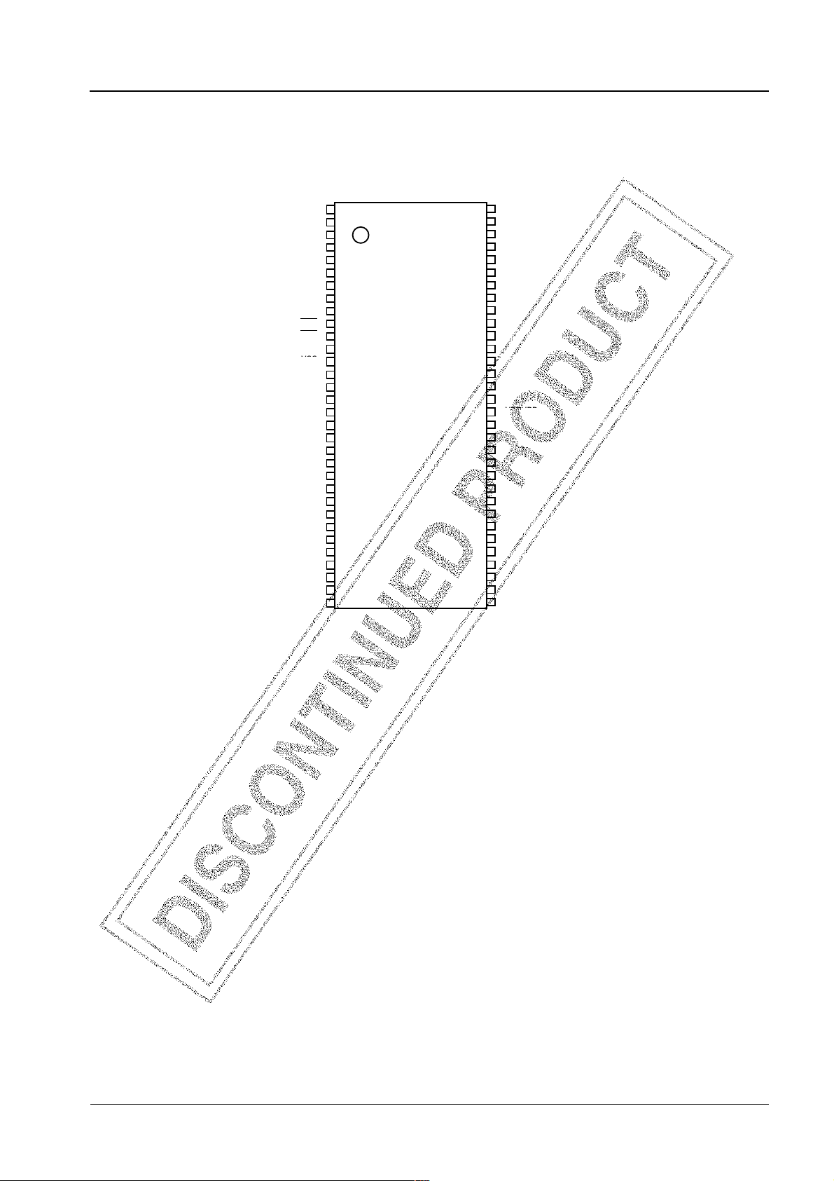
Pin Assignments
DIP64S
P10/SO0
P11/SI0/SB0
P12/SCK0
P13/SO1
P14/SI1/SB1
P15/SCK1
P16/BUZ
P17/PWM
TEST1
RES
XT1/P74
XT2
VSS
V
CF1
CF2
VDD
V
P80/AN0
P81/AN1
P82/AN2
P83/AN3
P84/AN4
P85/AN5
P86/AN6
P87/AN7
P70/INT0
P71/INT1
P72/INT2/T0IN
P73/INT3/T0IN
P30
P31
P32
P33
LC865020B/16B/12B/08B
1
2
3
4
5
6
7
8
9
10
11
12
13
SS
14
15
DD
16
17
18
19
20
21
22
23
24
25
26
27
28
29
30
31
32
64
63
62
61
60
59
58
57
56
55
54
53
52
51
50
49
48
47
46
45
44
43
42
41
40
39
38
37
36
35
34
33
P07
P06
P05
P04
P03
P02
P01
P00
P27
P26
P25
P24
P23
P22
P21
P20
VDDVPP
VDDV
VSS
V
SS
P51
P50
P47
P46
P45
P44
P43
P42
P41
P40
P37
P36
P35
P34
PP
Top view
No. 5650-5/21
Page 6
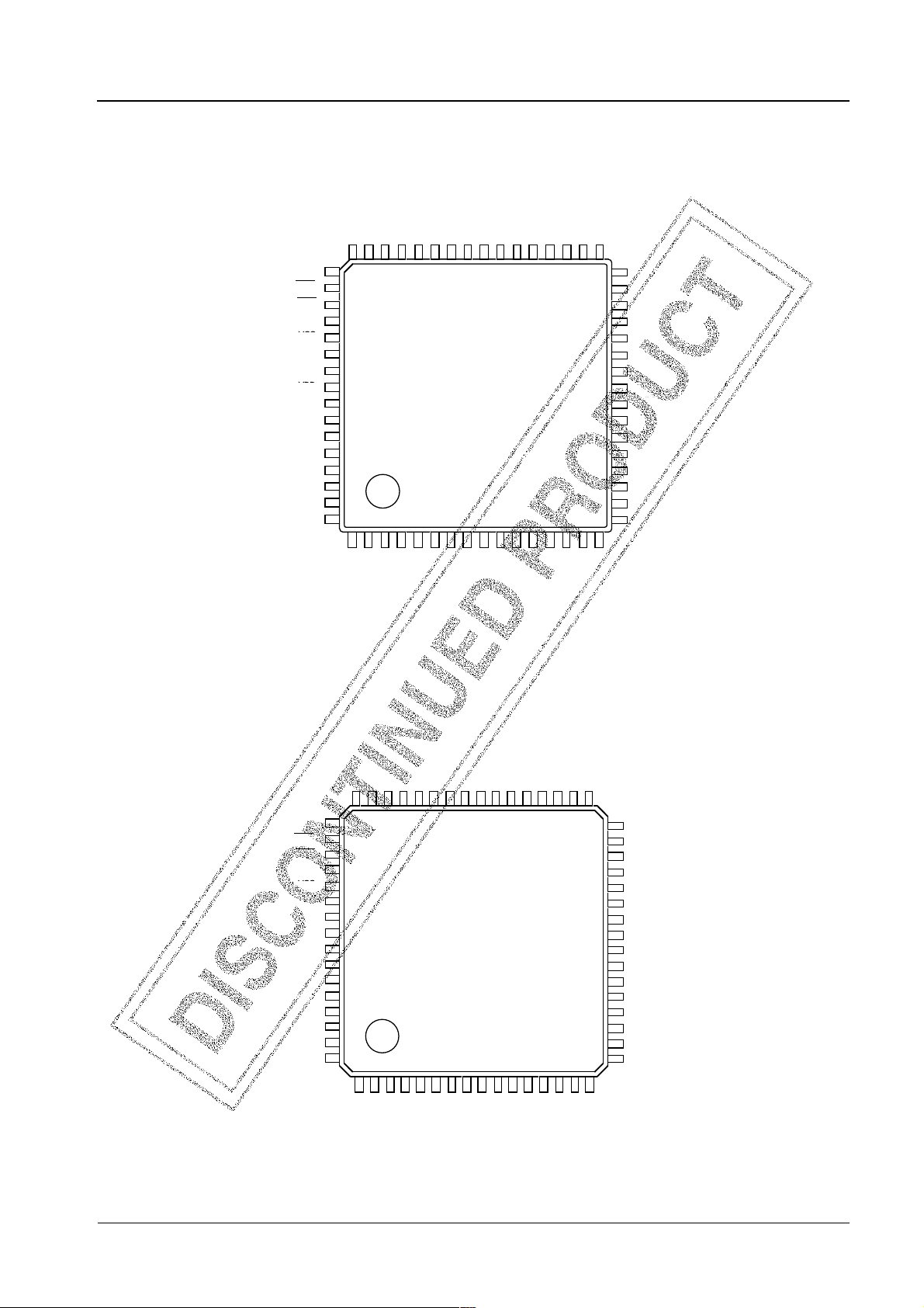
QFP64E
TEST1
RES
XT1/P74
XT2
VSS
CF1
CF2
VDD
P80/AN0
P81/AN1
P82/AN2
P83/AN3
P84/AN4
P85/AN5
P86/AN6
P87/AN7
LC865020B/16B/12B/08B
P00
P01
P02
P03
P04
P05
P06
P07
P10/SO0
P11/SI0/SB0
P12/SCK0
P13/SO1
P14/SI1/SB1
P15/SCK1
P16/BUZ
P17/PWM
48
49
46
47
50
51
52
V
V
53
SS
54
55
56
DD
57
58
59
60
61
62
63
123456789
64
45
42
43
44
39
40
41
10
38
121314
11
36
37
35
32
P27
33
34
31
30
29
28
27
26
25
24
23
22
21
20
19
18
15
17
P26
P25
P24
P23
P22
P21
P20
VDDVPP
VDDV
PP
VSS
V
SS
P51
P50
P47
P46
P45
P44
16
SQFP64
TEST1
RES
XT1/P74
XT2
VSS
V
CF1
CF2
VDD
V
P80/AN0
P81/AN1
P82/AN2
P83/AN3
P84/AN4
P85/AN5
P86/AN6
P87/AN7
P30
P31
P32
P33
P34
P35
P36
P37
P40
P41
P42
P43
P71/INT1
P70/INT0
Top view
P72/INT2/T0IN
P73/INT3/T0IN
P00
P01
P02
P03
P04
P05
P06
P07
P10/SO0
P11/SI0/SB0
P12/SCK0
P13/SO1
P14/SI1/SB1
P15/SCK1
P16/BUZ
P17/PWM
48
47
44
45
46
49
50
51
52
53
SS
54
55
DD
56
57
58
59
60
61
62
63
123456789
64
40
41
42
43
36
35
37
38
39
12
13
10
11
14
32
33
34
31
30
29
28
27
26
25
24
23
22
21
20
19
18
17
15
P27
P26
P25
P24
P23
P22
P21
P20
VDDVPP
VDDV
PP
VSS
V
SS
P51
P50
P47
P46
P45
P44
16
P71/INT1
P70/INT0
P72/INT2/T0IN
P30
P31
P32
P33
P73/INT3/T0IN
P34
P35
P36
P37
P40
P41
P42
P43
Top view
No. 5650-6/21
Page 7
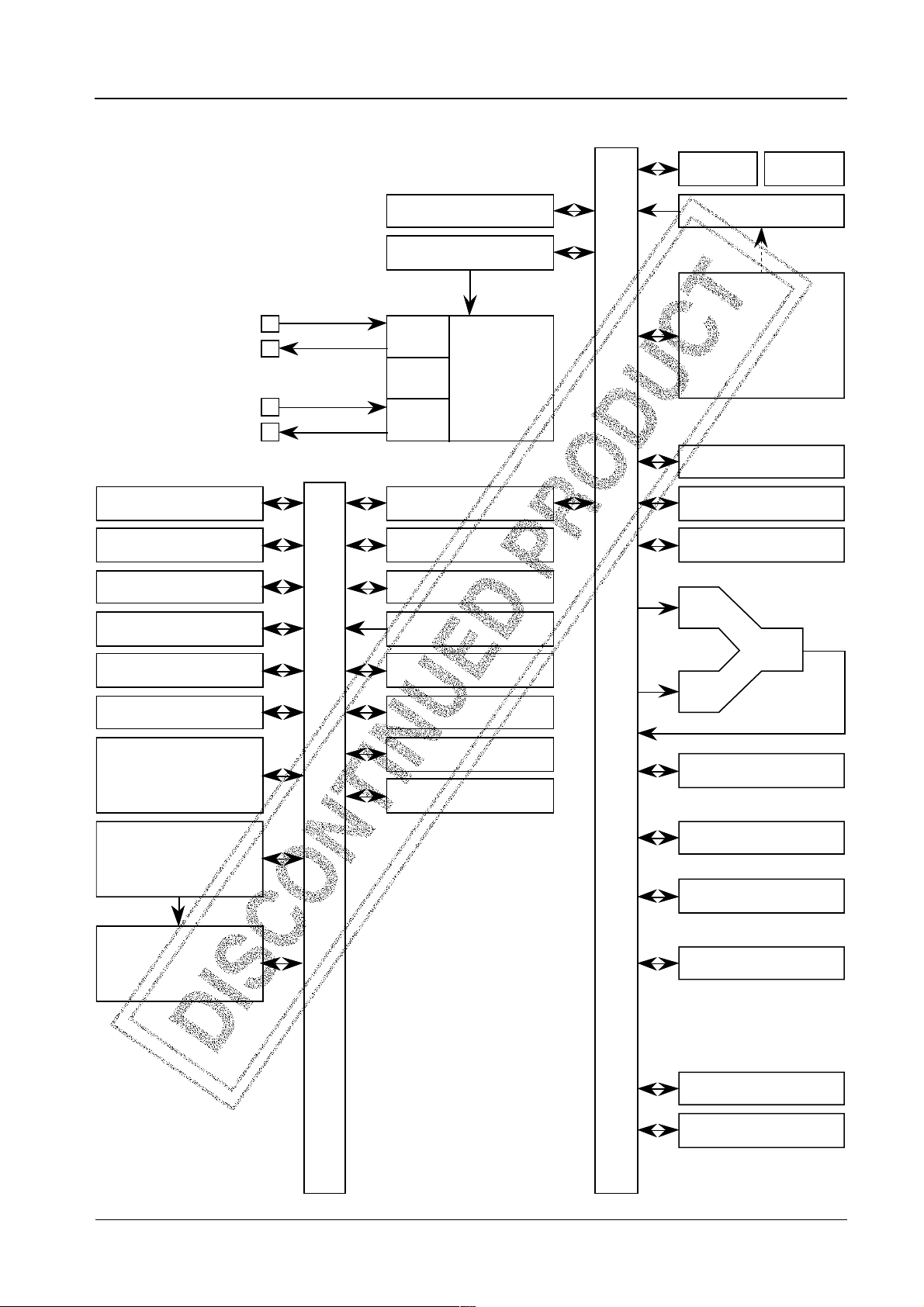
System Block Diagram
LC865020B/16B/12B/08B
IR PLA
Base timer
SIO0
SIO1
Timer 0
Timer 1
Bus
Interrupt control
Stand-by control
CF
RC
Clock
generator
X tal
Bus interface
Port1
Port7
Port8
Port2
Bus
ROM
PC
ACC
B register
C register
ALU
ADC
INT0 to 3
Noise rejection
filter
Real time
service
RAM
(128 bytes)
Port3
Port4
PSW
Port5
RAR
RAM
Stack pointer
PORT 0
Watchdog timer
No. 5650-7/21
Page 8

LC865020B/16B/12B/08B
r
ly
LC865020B/16B/12B/08B Pin Description
Pin name I/O Function description Option
V
SS
V
DD
VDDVPP* Power supply (+)
PORT0 I/O • 8-bit input/output port • Pull-up resistor :
P00 to P07 • Input for port 0 interrupt Present / Not present
PORT1 I/O • 8-bit input/output port • Output form :
P10 to P17 • Data direction can be specified for each bit. CMOS/N-channel open-drain
PORT2 I/O • 8-bit input/output port Output form :
P20 to P27 • Input/output in bit units CMOS/N-channel open-drain
PORT3 I/O • 8-bit input/output port • Pull-up resistor :
P30 to P37 • Input/output in bit units Present / Not present
PORT4 I/O • 8-bit input/output port • Pull-up resistor :
P40 to P47 • Input/output in bit units Present / Not present
PORT5 I/O • 2-bit input/output port • Pull-up resistor :
P50 , P51 • Input/output in bit units Present / Not present
Power supply (–)
Power supply (+)
• Data direction programmable in nibble units
• Input for HOLD release • Output form :
CMOS/N-channel open-drain
• Other pin functions
P10 SIO0 data output
P11 SIO0 data input /bus input/output
P12 SIO0 clock input/output
P13 SIO1 data output
P14 SIO1 data input /bus input/output
P15 SIO1 clock input/output
P16 Buzzer output
P17 Timer1 output (PWM output)
• 15 V withstand at N-channel open-drain output • Output form :
CMOS/N-channel open-drain
• 15 V withstand at N-channel open-drain output • Output form :
CMOS/N-channel open-drain
• 15 V withstand at N-channel open-drain output • Output form :
CMOS/N-channel open-drain
* Connect as in the following figure to reduce noise into VDD.
Short-circuit the V
Short-circuit the two V
terminal to the VDDVPP pin.
DD
pins.
SS
LSI
V
DD
VDD
Powe
Supp
VDDV
VDDVPP
PP
VSS
SS
VSS
V
SS
V
No. 5650-8/21
Page 9

LC865020B/16B/12B/08B
Pin name I/O Function description Option
PORT7 • 5-bit input port Pull-up resistor :
• Other pin functions Present / Not present
P70 I/O P70: INT0 input / HOLD release (P70,71,72,73)
/ N-channel Tr. output for watchdog timer * P74 does not have pull-up resistor option.
P71 to P74 I P71: INT1 input / HOLD release input
P72: INT2 input / timer 0 event input
P73: INT3 input with noise filter/timer 0 event input
P74: XT1 input pin for 32.768 kHz crystal
oscillator
• Interrupt received form, vector address
Rising Falling Rising High Low Vector
& level level
falling
INT0 Enable Enable Disable E nable Enable 03H
INT1 Enable Enable Disable E nable Enable 0BH
INT2 Enable Enable Enable Disable Disable 13H
INT3 Enable Enable Enable Disable Disable 1BH
PORT8 I • 8-bit input port
P80 to P87 • Other function
AD input port (8 port pins)
RES I Reset pin with pull-up resistor
TEST1 O • Test pin
Should be left open.
• Output fixed HIGH
XT1/P74 I • Input pin for 32.768 kHz crystal oscillator
• Other function
Input port P74
When not in use, connect to V
XT2 O Output pin for 32.768 kHz crystal oscillator
When not in use, should be left open.
CF1 I Input pin for ceramic resonator oscillator
CF2 O Output pin for ceramic resonator oscillator
• All port options can be specified for each bit.
DD
.
• State of pins at reset
Pin name Input/output mode State of pull-up resistor specified at pull-up option
Port 0 Input Fixed pull-up resistor exist
Ports 70, 71, 72, 73
Ports 1, 2 Input Programmable pull-up resistor OFF
Ports 3, 4, 5
No. 5650-9/21
Page 10

LC865020B/16B/12B/08B
Specifications
1. Absolute Maximum Ratings at Ta = 25°C , VSS = 0 V
Parameter Symbol Pins Conditions Ratings Unit
VDD[V] min typ max
Supply voltage VDD max VDD, VDDV
PP
Input voltage VI(1) • Ports 71, 72, 73, 74 –0.3 VDD+0.3
• Port 8
• RES
Input/output VIO(1) • Ports 0, 1, 2 –0.3 VDD+0.3
voltage • Ports 3, 4, 5 at
CMOS output option
VIO(2) Ports 3, 4, 5 at N-ch –0.3 +15
open-drain output
option
I
Highlevel
output
current
Peak
output
current
Total
output
current
(1) Ports 0, 1, 2, 3, 4, 5 CMOS output at each –4mA
OPH
∑I
(1) Ports 0, 1 Total of all pins –20
OAH
∑I
(2) Ports 2, 3, 4, 5 Total of all pins –20
OAH
VDD = VDDV
pin
PP
–0.3 +7.0 V
Lowlevel
output
current
Peak
output
current
Total
output
current
I
(1) Ports 0, 1, 2, 3, 4, 5 At each pin 20
OPL
I
(2) Port 70 At each pin 15
OPL
∑I
(1) Ports 0, 1 Total of all pins 40
OAL
Port 70
∑I
(2) Port 2 Total of all pins 40
OAL
∑I
(3) Ports 3, 4, 5 Total of all pins 80
OAL
Power dissipation Pd max (1) DIP64S Ta = –30 to +70°C 700 mW
(max.)
Pd max (2) QFP64E Ta = –30 to +70°C 420
Pd max (3) SQFP64 Ta = –30 to +70°C 290
Operating Topr –30 +70 °C
temperature
range
Storage Tstg –65 +150
temperature
range
No. 5650-10/21
Page 11

LC865020B/16B/12B/08B
2. Recommended Operating Ranges at Ta = –30°C to +70°C, VSS = 0 V
Parameter Symbol Pins Conditions Ratings Unit
VDD[V] min typ max
Operating voltage VDD(1) V
DD
range tCYC ≤ 400 µs
VDD(2) 3.9 µs ≤ tCYC 2.7 6.0
HOLD voltage V
HD
V
DD
Input high voltage VIH(1) Port 0 (Schmitt) Output disable 2.7 to 6.0 0.4V
VIH(2) • Ports 1, 2 Output disable 2.7 to 6.0 0.75V
• Ports 72, 73
(Schmitt)
VIH(3) • Port 70 Output N-channel 2.7 to 6.0 0.75V
Port input/interrupt transistor OFF
• Port 71
• RES (Schmitt)
VIH(4) Port 70 Output N-channel 2.7 to 6.0 0.9V
Watchdog timer transistor OFF
VIH(5) • Port 74 Output N-channel 27 to 6.0 0.75V
• Port 8 transistor OFF
VIH(6) Ports 3, 4, 5 of CMOS Output disable 4.0 to 6.0 0.75V
output (Schmitt)
VIH(7) Ports 3, 4, 5 of open- Output disable 4.0 to 6.0 0.75V
drain output
(Schmitt)
0.98 µs ≤ tCYC 4.5 6.0 V
tCYC ≤ 400 µs
RAM and Registers 2.0 6.0
hold voltage at HOLD
mode.
DD
V
+0.9
V
V
V
V
V
V
13.5
13.5
2.7 to 4.0 0.8V
2.7 to 4.0 0.8V
DD
DD
DD
DD
DD
DD
DD
DD
DD
DD
DD
DD
DD
DD
DD
Input low voltage VIL(1) Port 0 (Schmitt) Output disable 2.7 to 6.0 V
VIL(2) • Ports 1, 2, 3, 4, 5 Output disable 2.7 to 6.0 V
SS
SS
0.2V
0.25V
DD
DD
• Ports 72, 73
(Schmitt)
VIL(3) • Port 70 N-channel transistor 2.7 to 6.0 V
SS
0.25V
DD
Port input/interrupt OFF
• Port 71
• RES (Schmitt)
VIL(4) Port 70 N-channel transistor 2.7 to 6.0 V
SS
0.8V
DD
Watchdog timer OFF –1.0
VIL(5) • Port 74 Output N-channel 2.7 to 6.0 V
SS
0.25V
DD
• Port 8 transistor OFF
Operating cycle tCYC 4.5 to 6.0 0.98 400 µs
time 2.7 to 6.0 3.9 400
No. 5650-11/21
Page 12

LC865020B/16B/12B/08B
Parameter Symbol Pins Conditions Ratings Unit
VDD[V] min typ max
Oscillation FmCF(1) CF1, CF2 • 12 MHz (ceramic 4.5 to 6.0 11.76 12 12.24 MHz
frequency range resonator oscillation).
(Note 1) • Refer to Figure 1.
FmCF(2) CF1, CF2 • 3 MHz (ceramic 2.7 to 6.0 2.94 3 3.06
resonator oscillation).
• Refer to Figure 1.
FmRC RC oscillation 2.7 to 6.0 0.4 0.8 3.0
FsXtal XT1, XT2 • 32.768 kHz (crystal 2.7 to 6.0 32.768 kHz
oscillation).
• Refer to Figure 2.
Oscillation stable tmsCF(1) CF1, CF2 • 12 MHz (ceramic 4.5 to 6.0 0.03 0.5 ms
time period resonator oscillation).
(Note 1) • Refer to Figure 3.
tmsCF(2) CF1, CF2 • 3 MHz (ceramic 4.5 to 6.0 0.2 2
resonator oscillation).
• Refer to Figure 3.
tssXtal XT1, XT2 • 32.768 kHz (crystal 4.5 to 6.0 1 1.5 s
oscillation).
• Refer to Figure 3.
(Note 1) Refer to Table 1 and Table 2 for oscillation constant.
2.7 to 6.0 0.2 6
2.7 to 6.0 1 3
No. 5650-12/21
Page 13

LC865020B/16B/12B/08B
3. Electrical Characteristics at Ta = –30°C to +70°C , VSS = 0 V
Parameter Symbol Pins Conditions Ratings Unit
VDD[V] min typ max
Input high current IIH(1) Ports 3, 4, 5 of open- • Output disabled 2.7 to 6.0 5 µA
drain output • V
IIH(2) • Port 0 without • Output disabled 2.7 to 6.0 1
pull-up MOS • Pull-up MOS
transistor transistor OFF.
• Ports 1, 2, 3, 4, 5 V
IIH(3) • Ports 70, 71, 72, 73 VIN = V
without pull-up
MOS transistor
• Port 8
IIH(4) RES VIN = V
Input low current IIL(1) • Ports 1, 2, 3, 4, 5 • Output disabled 2.7 to 6.0 –1
• Port 0 without • Pull-up MOS
pull-up MOS transistor OFF.
transistor V
IIL(2) • Ports 70, 71, 72, 73 VIN = V
without pull-up
MOS transistor
• Port 8
IIL(3) RES VIN = V
Output high VOH(1) Ports 1, 2, 3, 4, 5 IOH = –1 mA 4.5 to 6.0 VDD–1V
voltage
V
(2)
OH
of CMOS output
Output low VOL(1) Ports 1, 2, 3, 4, 5 IOL = 10 mA 4.5 to 6.0 1.5
voltage
V
(2) IOL = 1.6 mA 4.5 to 6.0 0.4
OL
VOL(3) • IOL = 1.0 mA 2.7 to 6.0 0.4
VOL(4) Port 70 IOL = 1 mA 4.5 to 6.0 0.4
VOL(5) IOL = 0.5 mA 2.7 to 6.0 0.4
Pull-up MOS Rpu • Ports 1, 2, 3, 4, 5 VOH = 0.9 V
transistor resistor • Ports 70, 71, 72, 73 2.7 to 4.5 25 70 150
Hysteresis voltage V
HIS
• Ports 1, 2, 3, 4, 5 Output disable 2.7 to 6.0 0.1V
• Ports 70, 71, 72, 73
• RES
Pin capacitance CP All pins • f = 1 MHz 2.7 to 6.0 10 pF
= 13.5 V
IN
(including off-state
leak current of the
output transistor)
= V
IN
DD
(including off-state
leak current of the
output transistor)
2.7 to 6.0 1
2.7 to 6.0 1
IN
= V
DD
DD
SS
(including off-state
leak current of the
output transistor)
SS
SS
2.7 to 6.0 –1
2.7 to 6.0 –1
IOH = –0.1 mA 2.7 to 6.0 VDD–0.5
• The current of any
unmeasured pin
is 1 mA or less.
DD
4.5 to 6.0 15 40 70 kΩ
Unmeasured input
pins are set to
level.
V
SS
• Ta = 25°C
DD
V
No. 5650-13/21
Page 14

LC865020B/16B/12B/08B
4. Serial Input/Output Characteristics at Ta = –30°C to +70°C, VSS = 0 V
Parameter Symbol Pins Conditions Ratings Unit
VDD[V] min typ max
Cycle
Low-
level
pulse
width
High-
Input clock
level
pulse
width
Cycle
Serial clock
Lowlevel
pulse
width
Output clock
Highlevel
pulse
width
Data setup tICK • SI0, SI1 • Set to the rise of 4.5 to 6.0 0.1 µs
time • SB0, SB1 SCK0, SCK1. 2.7 to 6.0 0.4
Data hold tCKI • Refer to Figure 5. 4.5 to 6.0 0.1
Serial input
time 2.7 to 6.0 0.4
Output delay tCKO(1) • SO0, SO1 • Use an external 4.5 to 6.0 7/12tCYC
time • SB0, SB1 pull-up resistor +0.2
(Serial clock (1 kΩ) with open-
is extrnal drain output. 2.7 to 6.0 7/12tCYC
clock.) +1
Output delay tCKO(2) • Set to the fall of 4.5 to 6.0 1/3tCYC
time SCK0, SCK1. +0.2
(Serial clock • Refer to Figure 5.
Serial output
is internal
clock.)
tCKCY(1) SCK0, SCK1 Refer to Figure 5. 2.7 to 6.0 2 tCYC
tCKL(1) 2.7 to 6.0 1
tCKH(1) 2.7 to 6.0 1
tCKCY(2) SCK0, SCK1 • Use an external 2.7 to 6.0 2
pull-up resistor
(1 kΩ) with open-
tCKL(2)
tCKH(2) 2.7 to 6.0 1/2tCKCY
drain output.
• Refer to Figure 5.
2.7 to 6.0 1/2tCKCY
2.7 to 6.0 1/3tCYC
+1
No. 5650-14/21
Page 15

LC865020B/16B/12B/08B
5. Pulse Input Conditions at Ta = –30°C to +70°C , VSS = 0 V
Parameter Symbol Pins Conditions Ratings Unit
VDD[V] min typ max
High/low-level tPIH(1) • INT0, INT1 • Interrupt acceptable 2.7 to 6.0 1 tCYC
pulse width tPIL(1) • INT2/T0IN • Timer/counter 0
• INT3 pulse countable
tPIH(2) INT3/T0IN Interrupt acceptable 2.7 to 6.0 2
tPIL(2) (Noise rejection filter
time constant is 1/1.)
tPIH(3) INT3/T0IN Interrupt acceptable 2.7 to 6.0 32
tPIL(3) (Noise rejection filter
time constant is 1/16.)
tPIL(4) RES Reset acceptable 2.7 to 6.0 200 µs
6. A/D Converter Characteristics at Ta = –30°C to +70°C , VSS = 0 V
Parameter Symbol Pins Conditions Ratings Unit
VDD[V] min typ max
Resolution N 4.5 to 6.0 8 bit
Absolute precision ET 4.5 to 6.0 ±1.5 LSB
(Note 2)
Conversion time tCAD A/D conversion time 4.5 to 6.0 15.68 65.28 µs
= 16 × tCYC (tCYC = (tCYC =
(ADCR2 = 0) 0.98 µs) 4.08 µs)
(Note 3)
A/D conversion time 31.36 130.56
= 32 × tCYC (tCYC = (tCYC =
(ADCR2 = 1) 0.98 µs) 4.08 µs)
(Note 3)
Analog input V
AIN
voltage range
Analog port I
input current I
AINH
AINL
(Note 2) Quantizing error (±1/2 LSB) is not included.
(Note 3) Conversion time is the period from execution of instruction starting the conversion to completion of shifting the A/D
converted value to the register.
AN0 to AN7 4.5 to 6.0 V
V
= V
AIN
DD
V
= V
AIN
SS
4.5 to 6.0 +1 µA
4.5 to 6.0 –1
SS
V
DD
V
No. 5650-15/21
Page 16

LC865020B/16B/12B/08B
7. Current Drain Characteristics at Ta = –30°C to +70°C, VSS = 0 V
Parameter Symbol Pins Conditions Ratings Unit
VDD[V] min typ max
Current drain I
during basic for ceramic resonator
operation oscillation.
(Note 4) • FsXtal = 32.768 kHz
DDOP
(1) V
DD
• FmCF = 12 MHz 4.5 to 6.0 10 20 mA
for crystal oscillator.
• System clock :
CF oscillator
• Internal RC
oscillator stopped.
I
(2) • FmCF = 3 MHz 4.5 to 6.0 3 7
DDOP
for ceramic resonator
oscillation.
• FsXtal = 32.768 kHz
for crystal oscillator.
• System clock :
CF oscillator
• Internal RC
I
(3) oscillator stopped. 2.7 to 4.5 1.5 5
DDOP
I
(4) • FmCF = 0 Hz 4.5 to 6.0 0.7 3.0
DDOP
(when oscillator
stops).
• FsXtal = 32.768 kHz
for crystal oscillator.
• System clock :
I
(5) RC oscillator 2.7 to 4.5 0.4 2.5
DDOP
I
(6) • FmCF = 0 Hz 4.5 to 6.0 35 100 µA
DDOP
(when oscillator
stops).
• FsXtal = 32.768 kHz
for crystal oscillator.
• System clock :
32.768 kHz
• Internal RC
I
(7) oscillator stopped. 2.7 to 4.5 15 50
DDOP
No. 5650-16/21
Page 17

LC865020B/16B/12B/08B
Parameter Symbol Pins Conditions Ratings Unit
VDD[V] min typ max
Current drain at I
HALT mode • FmCF = 12 MHz
(Note 4) for ceramic resonator
Current drain at I
HOLD mode
(Note 4)
(Note 4) The currents to output transistors and pull-up MOS transistors are ignored.
DDHALT
(1) V
DD
• HALT mode 4.5 to 6.0 5 10 mA
oscillation.
• FsXtal = 32.768 kHz
for crystal oscillatior.
• System clock :
CF oscillator.
• Internal RC
oscillator stopped.
I
(2) • HALT mode 4.5 to 6.0 2.2 4.6
DDHALT
FmCF = 3 MHz
for ceramic resonator
oscillation.
• FsXtal = 32.768 kHz
for crystal oscillator.
• System clock :
CF oscillator.
• Internal RC
(3) oscillator stopped. 2.7 to 4.5 0.8 2.5
I
DDHALT
I
(4) • HALT mode 4.5 to 6.0 400 1000 µA
DDHALT
FmCF = 0 Hz
(when oscillator
stops).
• FsXtal = 32.768 kHz
for crystal oscillator.
• System clock :
(5) RC oscillator 2.7 to 4.5 200 750
I
DDHALT
I
(6) • HALT mode 4.5 to 6.0 25 100
DDHALT
FmCF = 0 Hz
(when oscillator
stops).
• FsXtal = 32.768 kHz
for crystal oscillator.
• System clock :
32.768 kHz
• Internal RC
(7) oscillator stopped. 2.7 to 4.5 8 40
I
DDHALT
(1) V
DDHOLD
I
DDHOLD
DD
(2) 2.7 to 4.5 0.02 20
HOLD mode 4.5 to 6.0 0.05 30
No. 5650-17/21
Page 18

LC865020B/16B/12B/08B
Oscillation type Supplier Oscillator C1 C2
12 MHz ceramic resonator Murata CSA12.0MTZ 33 pF 33 pF
oscillation
Kyocera KBR-12.0M 33 pF 33 pF
3 MHz ceramic resonator Murata CSA3.00MG040 100 pF 100 pF
oscillation
Kyocera KBR-3.0MS 47 pF 47 pF
* K rank (±10%) and SL characteristics must be used for C1 and C2.
Table 1. Ceramic Resonator Oscillation Guaranteed Constants (Main clock)
Oscillation type Supplier Oscillator C3 C4
32.768 kHz crystal oscillation Kyocera KF-38G-13P0200 18 pF 18 pF
* J rank (±5%) and CH characteristics must be used for C3 and C4.
(For applications which do not need high precision, use K rank (±10%) and SL characteristics.)
Table 2. Crystal Oscillation Guaranteed Constants (Sub-clock)
Notes • Since the circuit pattern affects the oscillation frequency, place the oscillation-related parts as close to the oscillator
pins as possible with the shortest pattern length.
• If other oscillators are used, we provide no guarantee for the characteristics.
CST12.0MTW On chip
CST3.00MGW040 On chip
CF1
C1
Figure 1 Ceramic Resonator Oscillator
CF
Main-clock circuit
CF2
C2
XT1 XT2
X tal
C3
Sub-clock circuit
Figure 2 Crystal Oscillator
C4
No. 5650-18/21
Page 19

Power supply
RES
Internal RC
resonator oscillation
CF1, CF2
XT1, XT2
LC865020B/16B/12B/08B
Reset time
t
msCF
t
ssXtal
V
DD
VDD lower limit
0 V
Operation mode
HOLD release signal
Internal RC
resonator oscillation
CF1, CF2
XT1, XT2
Operation mode
<HOLD release signal and oscillation stable time.>
Unfixed
Reset
Instruction execution mode
<Reset time and oscillation stable time.>
Valid
t
msCF
t
ssXtal
HOLD
Figure 3 Oscillation Stable Time
Instruction execution mode
RES
VDD
V
DD
R
RES
Values of C
(Note) Fix the value of C
that reset time is at least 200 µs, measured
C
RES
sure to reset untill 200µs, after Power supply
from the point when V
has been over inferior limit of supply voltage.
limit.
Figure 4 Reset Circuit
RES
and R
should be set such
RES
RES
, R
RES
exceeds VDD lower
DD
that is
No. 5650-19/21
Page 20

LC865020B/16B/12B/08B
0.5VDD
0.5V
< AC timing point >
t
CKCY
t
CKL
DD
t
CKH
V
VDD
DD
SCK0
SCK1
SI0
SI1
SO0,SO1
SB0,SB1
t
CKO
t
t
ICK
< Timing >
Figure 5 Serial Input/Output Test Conditions
t
PIL
CKI
t
PIH
1kΩ
50pF
< Test load >
Figure 6 Pulse Input Timing Conditions
No. 5650-20/21
Page 21

LC865020B/16B/12B/08B
Any and all SANYO products described or contained herein do not have specifications that can handle
applications that require extremely high levels of reliability, such as life-support systems, aircraft’s
control systems, or other applications whose failure can be reasonably expected to result in serious
physical and/or material damage. Consult with your SANYO representative nearest you before using
any SANYO products described or contained herein in such applications.
SANYO assumes no responsibility for equipment failures that result from using products at values that
exceed, even momentarily, rated values (such as maximum ratings, operating condition ranges, or other
parameters) listed in products specifications of any and all SANYO products described or contained
herein.
Specifications of any and all SANYO products described or contained herein stipulate the performance,
characteristics, and functions of the described products in the independent state, and are not guarantees
of the performance, characteristics, and functions of the described products as mounted in the customer’s
products or equipment. To verify symptoms and states that cannot be evaluated in an independent device,
the customer should always evaluate and test devices mounted in the customer’s products or equipment.
SANYO Electric Co., Ltd. strives to supply high-quality high-reliability products. However, any and all
semiconductor products fail with some probability. It is possible that these probabilistic failures could
give rise to accidents or events that could endanger human lives, that could give rise to smoke or fire,
or that could cause damage to other property. When designing equipment, adopt safety measures so
that these kinds of accidents or events cannot occur. Such measures include but are not limited to protective
circuits and error prevention circuits for safe design, redundant design, and structural design.
In the event that any or all SANYO products(including technical data,services) described or
contained herein are controlled under any of applicable local export control laws and regulations,
such products must not be exported without obtaining the export license from the authorities
concerned in accordance with the above law.
No part of this publication may be reproduced or transmitted in any form or by any means, electronic or
mechanical, including photocopying and recording, or any information storage or retrieval system,
or otherwise, without the prior written permission of SANYO Electric Co. , Ltd.
Any and all information described or contained herein are subject to change without notice due to
product/technology improvement, etc. When designing equipment, refer to the “Delivery Specification”
for the SANYO product that you intend to use.
Information (including circuit diagrams and circuit parameters) herein is for example only ; it is not
guaranteed for volume production. SANYO believes information herein is accurate and reliable, but
no guarantees are made or implied regarding its use or any infringements of intellectual property rights
or other rights of third parties.
This catalog provides information as of October, 1997. Specifications and information herein are subject to change without notice.
No. 5650-21/21
 Loading...