

Page 1

Ordering number: EN 5550
SANYO Electric Co.,Ltd. Semiconductor Bussiness Headquarters
TOKYO OFFICE Tokyo Bldg., 1-10, 1 Chome, Ueno, Taito-ku, TOKYO, 110-8534 JAPAN
LC86P4164
CMOS LSI
LC86P4164
8-bit Single Chip Microcontroller
Overview
The LC86P4164 is a CMOS 8-bit single chip microcontroller
with one-time PROM for the LC864100 series.
This microcontroller has the function and the pin description of
the LC864100 series mask ROM version, and the 64K-byte
PROM. It is suitable for developing programs.
Package Dimensions
unit : mm
3128-DIP52S
Features
(1) Option switching by PROM data
The option function of the LC864100 series can be specified by the PROM data.
The functions of the trial pieces can be evaluated using the mass production board.
(2) Internal PROM capacity : 65512 bytes (for program data)
: 8192 × 12 bits (for character data)
(3) Internal RAM capacity : 384 bytes
[LC86P4164]
SANYO : DIP52S
Mask ROM version PROM capacity RAM capacity
LC864164 65512 bytes 384 bytes
LC864156 57344 bytes 384 bytes
LC864148 49152 bytes 384 bytes
LC864140 40960 bytes 384 bytes
LC864132 32768 bytes 384 bytes
LC864124 24576 bytes 384 bytes
LC864120 20480 bytes 384 bytes
LC864116 16384 bytes 384 bytes
LC864112 12288 bytes 384 bytes
(4) Operating supply voltage : 4.5 V to 5.5 V
(5) Instruction cycle time : 1.0 µs to 30 µs
(6) Operating temperature : –30°C to +70°C
(7) The pin and the package compatible with the LC864100 series mask ROM devices
(8) Applicable mask ROM version : LC864164/LC864156/LC864148/LC864140/LC864132
LC864124/LC864120/LC864116/LC864112
(9) Factory shipment : DIP52S
SANYO Electric Co., Ltd. Semiconductor LSI Div. Microcontroller Development Dep.
33098HA (II)
No. 5550-1/20
Page 2
LC86P4164
Usage Notes
The LC86P4164 is provided for the first release and small shipping of the LC864100 series.
At using, take notice of the followings.
(1) Differences between the LC86P4164 and the LC864100 series
Item LC86P4164 LC864164/56/48/40/32/24/20/16/12
Operation after reset The option is specified by degrees until The program is executed from 00H of the
releasing 3 ms after going to a 'H' level to the reset program counter immediately after
terminal. The program is executed from going to a 'H' level to the reset terminal.
00H of the program counter.
Operating supply 4.5 V to 6.0 V 4.5 V to 6.0 V
voltage range (V
Operating temperature –30 to +70°C –30 to +70°C
range (Topr)
Power dissipation Refer to 'electrical characteristics' on the semiconductor news.
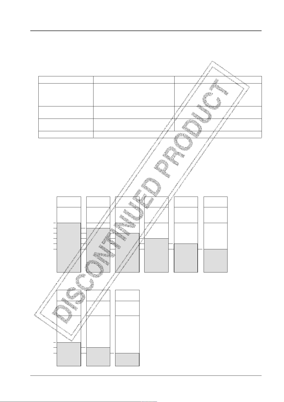
The LC86P4164 uses the program memory area of 256 bytes from FF00H to FFFFH to select the options.
(2) Option
The option data is created by the option specified program "SU86K.EXE". The created option data is linked to the program
area by the linkage loader "L86K.EXE".
DD
)
(3) ROM space
The LC86P4164 and LC864100 series use the program memory area of 256 bytes from FF00H to FFFFH to select options.
The program memory has 65280 bytes from 0000H to FEFFH.
13FFFFH
0FFFFH
0FF00H
0FEFFH
0DFFFH
0BFFFH
09FFFH
07FFFH
05FFFH
0000H
13FFFFH
0FFFFH
Character
generator ROM
Option specified
area 256 bytes
Program area Program area Program area Program area Program area Program area
64K bytes 56K bytes 48K bytes 40K bytes 32K bytes 24K bytes
LC864164 LC864156 LC864148 LC864140 LC864132 LC864124
Character
generator ROM
Option specified
area 256 bytes
Character
generator ROM
Option specified
area 256 bytes
Character
generator ROM
Option specified
area 256 bytes
Character
generator ROM
Option specified
area 256 bytes
Character
generator ROM
Option specified
area 256 bytes
Character
generator ROM
Option specified
area 256 bytes
Character
generator ROM
Option specified
area 256 bytes
Character
generator ROM
Option specified
area 256 bytes
04FFFH
03FFFH
02FFFH
0000H
Program area Program area Program area
20K bytes 16K bytes 12K bytes
LC864120 LC864116 LC864112
No. 5550-2/20
Page 3
LC86P4164
How to use
(1) Create a programming data for LC86P4164
Programming data for EPROM of the LC86P4164 is required.
Debugged evaluation file (EVA file) must be converted to an INTEL-HEX formatted file (HEX file) with file converter
program, SU86K.EXE. The HEX file is used as the programming data for the LC86P4164.
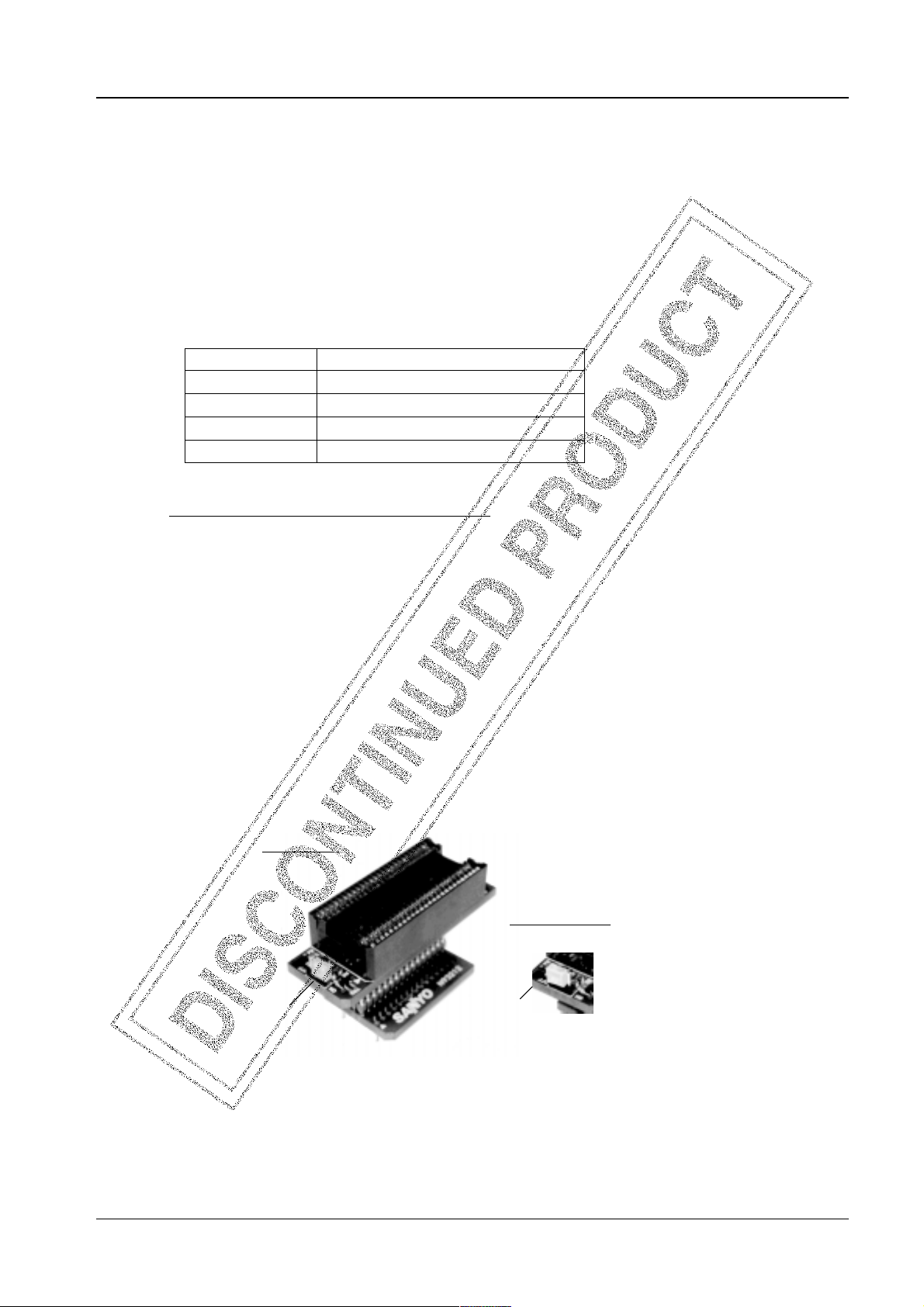
(2) How to program for the PROM
The LC86P4164 can be programmed by the EPROM programmer with attachment; W86EP4164D.
• Recommended EPROM programmer
Manufacturer EPROM progammer
Advantest R4945, R4944
Andou AF-9704
AVAL PKW-1100, PKW-3000
Minato electoronics MODEL 1890A
• "27010 (Vpp=12.5V) Intel high speed programming" mode should be adopted. The address must be set to "0 to 13FFFH"
and
a jumper (DASEC) must be set to 'OFF' at programming.
(3) How to use the data security function
"Data security" is the function to disable the EPROM data from being read out.
The following is the procedure in order to execute the data security function.
1. Set 'ON' the jumper of attachment.
2. Program again. Then the EPROM programmer displays an error. The error means that the data security functions
normally. It is not a trouble of the EPROM programmer or the LSI.
Notes
• Data security is not executed when the data of all address have 'FF' at the procedure 2 above.
• Data security cannot be executed by programming the sequential operation "BLANK=>PROGRAM=>VERIFY" at
procedure 2 above.
• Set the jumper to 'OFF' after executing the data security.
Data security
Data security OFF
Jumper
Jumper
W86EP4164D
pin 1
No. 5550-3/20
Page 4
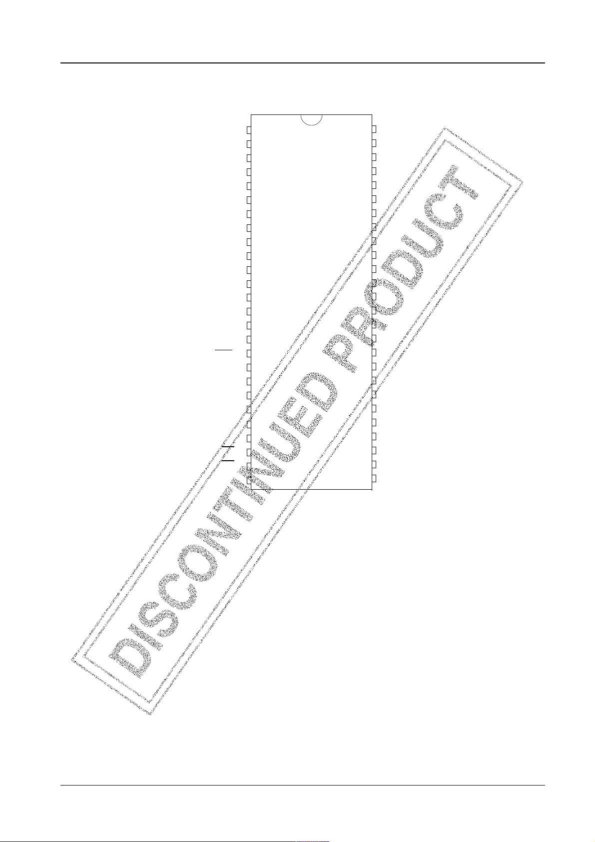
Pin Assignment
LC86P4164
P10/SO0
P11/SI0/SB0
P12/SCK0
P13
P14
P15
P16
P17/PWM
DVSS
CF1
CF2
DVDD
P90/AN0
P91/AN1
P92/AN2
P93/AN3
RES
LC1
LC2
FILT
AVDD
AVSS
CVIN
VS
HS
1
2
3
4
5
6
7
8
9
10
11
12
13
14
15
16
17
18
19
20
21
22
23
24
25
I
26
52
51
50
49
48
47
46
45
44
43
42
41
40
39
38
37
36
35
34
33
32
31
30
29
28
27
P07
P06
P05
P04
P03
P02
P01
P00
P73/INT3/T0IN
P72/INT2/T0IN
P71/INT1
P70/INT0
PWM9
PWM8
PWM7
PWM6
PWM5
PWM4
PWM3
PWM2
PWM1
PWM0
BL
B
G
R
Top view
No. 5550-4/20
Page 5
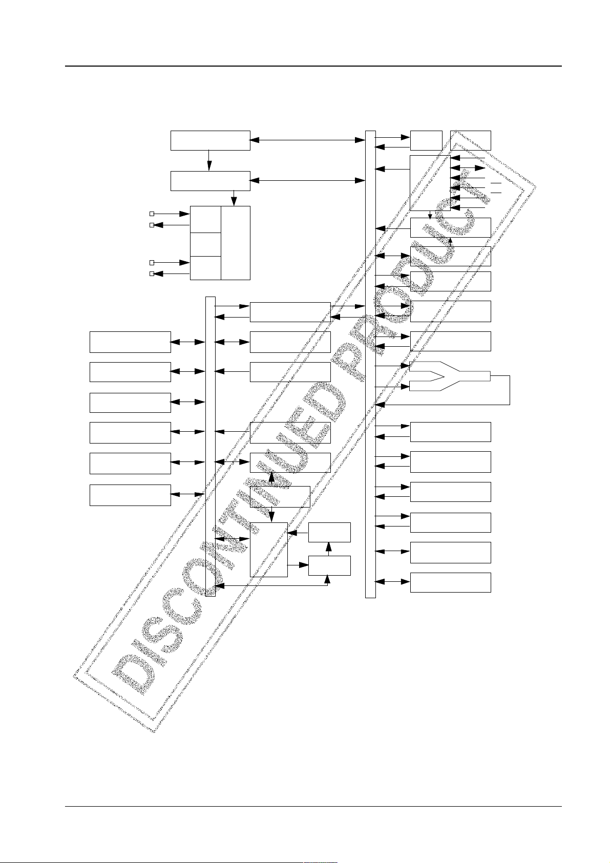
System Block Diagram
LC86P4164
SIO0
Timer 0
Timer 1
ADC
Interrupt control
Standby control
CF
RC
LC
Colck
generator
Bus interface
Port 1
Port 7
Port 9
IR PLA
PROM
control
PROM(64KB)
PC
ACC
B register
C register
ALU
PSW
A14 to A0
D7 to D0
TA
CE
OE
DASEC
INT0 to INT3
Noise rejection filter
PWM
Data slicer
PLL
OSD
control
circuit
RAR
RAM
Stack pointer
CGROM
Port 0
VRAM
Watchdog timer
No. 5550-5/20
Page 6
LC86P4164
Pin Description
Pin name Pin No. I/O Function description Option PROM mode
DVSS 9 — Negative power supply for digital circuit
CF1 10 I Input terminal for ceramic resonator
CF2 11 O Output terminal for ceramic resonator
DVDD 12 — Positive power supply for digital circuit
RES 17 I Reset terminal
LC1 18 I LC oscillation circuit input terminal
LC2 19 O LC oscillation circuit output terminal
FILT 20 O Filter terminal for PLL
AVDD 21 — Positive power supply for analog circuit
AVSS 22 — Negative power supply for analog circuit
CVIN 23 I Video signal input terminal
VS 24 I Vertical synchronization signal input
terminal
HS 25 I Horizontal synchronization signal input
terminal
I 26 O Image intensity control output
R 27 O Red (R) output terminal of RGB image A4 (*1)
output
G 28 O Green (G) output terminal of RGB image A5 (*1)
output
B 29 O Blue (B) output terminal of RGB image A6 (*1)
output
BL 30 O Fast blanking control signal A7 (*1)
Switch TV image signal and caption/
OSD image signal
PWM0 31 to 40 O PWM0 to PWM9 output terminal PWM0 to PWM8 :
to PWM9 15V withstand A8 to A16 (*1)
PWM9 : "L" fixed
Port 0 8-bit Input/output port Pull-up resistor
P00 to P07 45 to 52 I/O Input/output can be specified in nibble unit Provided/not provided
HOLD release input (in bit units)
Interrupt input Output Format
CMOS/Nch-OD
(in bit units)
Port 1 8-bit Input/output port Output Format D0 to D7 (*2)
P10 to P17 1 to 8 I/O Input/output can be specified in bit unit. CMOS/Nch-OD
Other functions (in bit unit)
P10 SIO0 data output
P11 SIO0 data input /bus input/output
P12 SIO0 clock input/output
P17 Timer 1 (PWM) output
Continued on next page.
No. 5550-6/20
Page 7

LC86P4164
Continued from preceding page.
Pin name Pin No. I/O Function Description Option PROM mode
Port 7 4-bit input port Pull-up resistor P70 : VPP (*3)
P70 41 I/O Other functions provided/ P71 : DASEC (*4)
P71 to P73 42 to 44 I not provided P72 : OE (*5)
Port 9 4-bit input port A0 to A3 (*3)
P90 to P93 13 to 16 I Other function
P70 INT0 input/HOLD release input/
Nch-transistor output for watchdog
timer
P71 INT1 input/HOLD release input
P72 INT2 input/timer 0 event input
P73 INT3 input (noise rejection filter
attached input/timer 0 event input
Interrupt receiver format vector address
Rising Falling Rising/Falling H level L level Vector
INT0 enable enable disable enable enable 03H
INT1 enable enable disable enable enable 0BH
INT2 enable enable enable disable disable 13H
INT3 enable enable enable disable disable 1BH
A/D converter input port (4 lines)
(in bit units) P73 : CE (*6)
*1 An → Address input
*2 Data I/O
*3 Power for programming
*4 Memory select input/output for data security
*5 Output Enable input
*6 Chip Enable input
All of port options except the 4-bit unit pull-up resistor option of Port 0 can be specified in a bit unit.
•
• Port status during reset
Terminal I/O Pull-up resistor status at selecting pull-up option
Port 0 Input Pull-up resistor OFF, ON after reset release
Port 1 Input Programmable pull-up resistor OFF
Port 7 Input Fixed pull-up resistor provided
* AVDD and AVSS are the power supply terminals for built-in analog circuit while DVDD and DVSS are the power supply
terminals for built-in digital circuit. Connect them like the following figure to reduce the mutual noise influence.
LSI
Power
Power
Supply
supply
DVDD
DVSS
AVDD
AVSS
No. 5550-7/20
Page 8

Specifications
LC86P4164
1. Absolute Maximum Ratings at Ta = 25
°
C, VSS = 0 V
Parameter Symbol Pins Conditions Ratings Unit
VDD [V] min typ max
Supply voltage VDDmax DVDD, AVDD DVDD = AVDD –0.3 +7.0 V
Input voltage VI(1) –0.3 VDD+0.3
• P71, 72, 73
• Port 9
• RES,HS,VS,CVIN
Output voltage VO(1) R, G, B, BL, I, FILT –0.3 VDD+0.3
VO(2) PWM0 to PWM9 –0.3 +15
Input/output
VIO(1) Ports 0, 1, P70 –0.3 VDD+0.3
voltage
Highlevel
output
current
Peak
output
current
I
(1) Ports 0, 1 –2mA
OPH
• Pull-up MOS
transistor output
• At each pin
I
(2) Ports 0, 1 –4
OPH
• CMOS output
• At each pin
I
(3) R, G, B, BL, I –5
OPH
• CMOS output
• At each pin
Lowlevel
output
current
Total
output
current
Peak
output
current
∑I
(1) Port 1 The total of all pins –10
OAH
∑I
(2) Port 0 The total of all pins –10
OAH
∑I
(3) R, G, B, BL, I The total of all pins –15
OAH
I
(1) Ports 0, 1 At each pin 20
OPL
I
(2) P70 At each pin 30
OPL
I
(3) • R, G, B, BL, I At each pin 5
OPL
• PWM0 to PWM9
Total
output
current
Maximum power
∑I
(1) Port 0 The total of all pins 40
OAL
∑I
(2) Port 1, P70 The total of all pins 40
OAL
∑I
(3) R, G, B, BL, I The total of all pins 15
OAL
∑I
(4) PWM0 to PWM9 The total of all pins 30
OAL
Pd max DIP52S Ta = –30 to +70°C 430 mW
dissipation
Operating
Topr –30 +70 °C
temperature range
Storage
Tstg –55 +125
temperature range
* DVSS and AVSS must be supplied the same voltage, VSS.V
DVDD and AVDD must be supplied the same voltage, V
.VDD = DVDD = AVDD
DD
= DVSS = AVSS
SS
No. 5550-8/20
Page 9

LC86P4164
2. Recommended Operating Range at Ta = –30°C to +70°C, VSS = 0 V
Parameter Symbol Pins Conditions Ratings Unit
VDD [V] min typ max
Operating
supply
voltage range
Hold voltage V
Input high-level VIH(1) Port 0 (Schmitt) 4.5 to 5.5 0.6V
voltage
Input low-level VIL(1) Port 0 (Schmitt) 4.5 to 5.5 V
voltage
CVIN input
amplitude
Operation cycle
time
V
DD
DVDD, AVDD 0.98 µs ≤ tCYC 4.5 5.5 V
tCYC ≤ 1.02 µs
HD
DVDD, AVDD 2.0 5.5
RAMs and the
registers hold data at
HOLD mode.
Output disable
VIH(2) • Port 1 (Schmitt) 4.5 to 5.5 0.75V
Output disable
DD
DD
V
V
• P72,73
• HS,VS
VIH(3) 4.5 to 5.5 0.75V
• P70
port input / interrupt
Output N-channel
transistor OFF
DD
V
• P71
• RES (Schmitt)
VIH(4) 4.5 to 5.5 VDD-0.5 V
P70 Watchdog timer
input
VIH(5) Port 9 port input 4.5 to 5.5 0.7V
VIL(2) • Port 1 (Schmitt) 4.5 to 5.5 V
Output N-channel
transistor OFF
Output disable
Output disable
DD
SS
SS
V
0.2V
0.25V
• P72,73
• HS,VS
• Port 9
VIL(3) 4.5 to 5.5 V
• P70 port input /
interrupt
N-channel transistor
OFF
SS
0.25V
• P71
• RES (Schmitt)
VIL(4) 4.5 to 5.5 V
P70
Watchdog timer input
VIL(5) Port 9 4.5 to 5.5 V
N-channel transistor
OFF
SS
SS
0.6V
0.3V
port input
V
CVIN
CVIN 5.0 0.7 2.3 Vp-p
tCYC(1) OSD function 4.5 to 5.5 0.98 1 1.02 µs
tCYC(2) Except OSD function 4.5 to 5.5 0.98 30
DD
DD
DD
DD
DD
DD
DD
DD
DD
DD
*
* Vp-p : Peak-to-peak voltage
No. 5550-9/20
Page 10

LC86P4164
Parameter Symbol Pins Conditions Ratings Unit
VDD [V] min typ max
Oscillation
frequency range
(Note 1)
Oscillation
stable time
period (Note 2)
FmCF CF1, CF2 4.5 to 5.5 11.76 12 12.24 MHz
FmLC LC1, LC2 4.5 to 5.5 14.11
FmRC 4.5 to 5.5 0.4 0.8 2.0
tmsCF CF1, CF2 4.5 to 5.5 0.02 0.2 ms
(Note 1) The oscillation constant is shown on Table 1 and Table 2.
(Note 2) The oscillation stable time period means the time to oscillate stably after the following conditions.
1. Supplying voltage.
2. Release the HOLD mode.
3. Release stopping the main-clock oscillation.
Refer to Figure 3 for details.
12MHz (ceramic
resonator oscillation)
Refer to Figure 1.
14.11MHz
(LC oscillation)
Refer to Figure 2.
RC oscillation
12 MHz (ceramic
resonator oscillation)
Refer to Figure 3.
No. 5550-10/20
Page 11

LC86P4164
3. Electrical Characteristics at Ta = –30°C to +70°C , VSS = 0 V
Parameter Symbol Pins Conditions Ratings Unit
VDD[V] min typ max
Input high-level
current
Input low-level
current
Output high-level
voltage
IIH(1) 4.5 to 5.5 1 µA
• Port 1
• Port 0 without
pull-up MOS
transistor
IIH(2) 4.5 to 5.5 1
• Port 7 without
pull-up MOS
transistor
• Port 9
• RES
• HS,VS
IIL(1) 4.5 to 5.5 –1
• Port 1
• Port 0 without
pull-up MOS
transistor
IIL(2) 4.5 to 5.5 –1
• Port 7 without
pull-up MOS
transistor
• Port 9
IIL(3) 4.5 to 5.5 –1
• RES
• HS,VS
VOH(1) 4.5 to 5.5 VDD–1V
CMOS output of
Ports 0,1
VOH(2) 4.5 to 5.5 VDD–0.5
R, G, B, BL, I
• Output disable
• Pull-up MOS
transistor OFF
• V
= VDD (including
IN
the off-leak current of
the output transistor)
V
= V
IN
DD
• Output disable
• Pull-up MOS
transistor OFF
• V
= VSS (including
IN
the off-leak current of
the output transistor)
V
= V
IN
SS
VIN = V
SS
IOH = –1.0 mA
I
= –0.1 mA
OH
Output low-level
voltage
Pull-up MOS
transistor
resistance
Output offleakage
current
Hysteresis
voltage
VOL(1) 4.5 to 5.5 1.5
VOL(2) 4.5 to 5.5 0.4
Ports 0, 1
Ports 0, 1
I
= 10 mA
OL
• I
OL
= 1.6 mA
• The total current of
the ports 0,1 is not
over 40 mA
VOL(3) 4.5 to 5.5 0.4
• R, G, B, BL, I
• PWM0 to PWM9
• I
= 30 mA
OL
• The current of any
unmesurement pin is
not over 3 mA.
VOL(4) 4.5 to 5.5 0.4
Rpu 4.5 to 5.5 13 38 80 kΩ
P70
• Ports 0,1
V
I
OL
= 1 mA
= 0.9 V
OH
DD
• Port 7
I
V
OFF
HIS
PWM0 to PWM9
• Ports 0,1
• Port 7
V
= 13.5 V
OUT
Output disable
4.5 to 5.5 5 µA
4.5 to 5.5 0.1 V
DD
• RES
• HS,VS
V
No. 5550-11/20
Page 12

LC86P4164
Parameter Symbol Pins Conditions Ratings Unit
VDD[V] min typ max
Input clamp
voltage
Pin capacitance • f = 1 MHz
4. Serial Input/Output Characteristics at Ta = –30°C to +70°C , VSS = 0 V
Parameter Symbol Pins Conditions Ratings Unit
Cycle
Low-
level
pulse
width
High-
Input clock
level
pulse
width
Cycle
Low-
Serial clock
Serial input
level
pulse
width
High-
Output clock
level
pulse
width
Data set-up
time
Data hold
time
V
CLMP
CP All pins 4.5 to 5.5 10 pF
tCKCY (1) 4.5 to 5.5 2 tCYC
tCKCY (1) 4.5 to 5.5 1
tCKCY (1) 4.5 to 5.5 1
tCKCY (2) 4.5 to 5.5 2
tCKCY (2) 4.5 to 5.5 1/2tCKCY
tCKCY (2) 4.5 to 5.5 1/2tCKCY
tICK 4.5 to 5.5 0.1 µs
tCKI 4.5 to 5.5 0.1
CVIN 5.0 2.3 2.5 2.7 V
• Unmeasured input
pins are set to
V
level.
SS
• Ta = 25°C
VDD[V] min typ max
• SCK0
• SCLK0
• SCK0
• SCLK0
SI0
Refer to Figure 5.
• Use a pull-up
resistor (1 kΩ)
during open drain
output
• Refer to Figure 5.
• Data set-up to SCK0
rising
• Data hold from
SCK0 rising
• Refer to Figure 5.
Output delay
time
(External
serial clock)
Output delay
time
Serial output
(Internal
serial clock)
tCKO(1) 4.5 to 5.5 7/12tCYC µs
tCKO(2) 4.5 to 5.5 1/3tCYC
SO0
• Use a pull-up
resistor (1 kΩ)
during open drain
output.
• Data set-up to SCK0
falling
• Data hold from
SCK0 falling
• Refer to Figure 5.
+0.2
+0.2
No. 5550-12/20
Page 13

LC86P4164
5. Pulse Input Conditions at Ta = –30°C to +70°C, VSS = 0 V
Parameter Symbol Pins Conditions Ratings Unit
VDD [V] min typ max
High/low level
pulse width
Rising/falling time
Horizontal
pull-in range
tPIH(1) 4.5 to 5.5 1 tCYC
tPIL(1)
tPIH(2) 4.5 to 5.5 2
tPIL(2)
• INT0,INT1
• INT2/T0IN
INT3/T0IN
(The noise
rejection clock is
selected to 1/1)
tPIH(3) 4.5 to 5.5 32
tPIL(3)
INT3/T0IN
(The noise
rejection clock is
selected to 1/16)
tPIL(4) 4.5 to 5.5 200 µs
tPIH(5) 4.5 to 5.5 10 tCYC
RES
HS, VS
tPIL(5)
tTHL 4.5 to 5.5 500 ns
HS
tTLH
FH 4.5 to 5.5 15.23 15.73 16.23 kHz
HS
• Interrupt acceptable
• Timer0-countable
• Interrupt acceptable
• Timer0-countable
• Interrupt acceptable
• Timer0-countable
Reset acceptable
Display position
controllable
Each active edge of
HS, VS must be more
than 1tCYC.
Refer to Figure 7.
Refer to Figure 7.
The monitor point in
Figure 10 is 1/2 V
DD
.
6. A/D Converter Characteristics at Ta = –30°C to +70°C, VSS = 0 V
Parameter Symbol Pins Conditions Ratings Unit
VDD [V] min typ max
Resolution
Absolute precision
Conversion time
Reference current
Analog input
voltage range
Analog port input
current
(Note 3) Absolute precision excepts quantizing error (±1/2 LSB).
N
ET
tCAD
I
REF
V
AIN
I
AINH
I
AINL
From selecting
Vref to resulting
AN0 to AN3
4.5 to 5.5 4 bit
(Note 3) 4.5 to 5.5 ± 1/4 ± 1/2 LSB
1 bit conversion time
4.5 to 5.5 1.96 µs
= 2tCYC
(Regulate the ladder
4.5 to 5.5 1.0 2.0 mA
resistor)
4.5 to 5.5 V
= V
V
AIN
DD
V
= V
AIN
SS
4.5 to 5.5 1 µA
4.5 to 5.5 –1
SS
V
DD
V
No. 5550-13/20
Page 14

LC86P4164
7. Current Dissipation Characteristics at Ta = –30°C to +70°C , VSS = 0 V
Parameter Symbol Pins Conditions Ratings Unit
VDD [V] min typ max
Current dissipation I
during basic
operation
(Note 4)
Current dissipation I
in HALT mode
(Note 4)
Current dissipation I
in HOLD mode
(Note 4)
(1) DVDD, AVDD 4.5 to 5.5 21 32 mA
DDOP
(1) DVDD, AVDD 4.5 to 5.5 5 10 mA
DDHALT
I
(2) DVDD, AVDD 4.5 to 5.5 400 800 µA
DDHALT
DDHOLD
DVDD, AVDD 4.5 to 5.5 0.05 20 µA
• FmCF = 12 MHz
Ceramic resonator
oscillation
• FmLC = 14.11 MHz
LC oscillation
• System clock :
CF oscillation
• Internal RC
oscillation stops
• HALT mode
• FmCF = 12 MHz
Ceramic resonator
oscillation
• FmLC = 0 Hz
(oscillation stops)
• System clock :
CF oscillation
• Internal RC
oscillation stops.
• HALT mode
• FmCF = 0 MHz
(oscillation stops)
• FmLC = 0 Hz
(oscillation stops)
• System clock :
Internal RC
• HOLD mode
• All oscillation stops.
(Note 4) The currents of the output transistors and the pull-up MOS transistors are ignored.
No. 5550-14/20
Page 15

LC86P4164
Oscillation type Manufacturer Oscillator C1 C2
12 MHz ceramic resonator Murata CSA12.0MTZ 33 pF 33 pF
oscillation CST12.0MTW on chip
Kyocera KBR-12.0M 47 pF 47 pF
* Both C1 and C2 must use an K rank (±10%) and an SL characteristics.
Table 1. Ceramic Resonator Oscillation Guaranteed Constant (main-clock)
Oscillation type L C3 C4
14.11 MHz LC oscillation 5.6 µH 27 pF 30 pF (Trimmer)
4.7 µH ± 10% 27 pH 27 pH
(Variable)
* See Figure 11,12.
Table 2. LC Oscillation Guaranteed Constant (OSD clock)
(Notes) • Since the circuit pattern affects the oscillation frequency, place the oscillation-related parts as close to
the oscillation pins as possible with the shortest possible pattern length.
• If you use other oscillators than those shown above, we provide no guarantee for the characteristics.
• Adjust the voltage of monitor point in Figure 10 to 1/2V
the PLL circuit.
± 10% by the LC oscillation constant 'L' or 'C' to lock
DD
CF1 CF2
CFC1 C2
Main clock
Figure 1 Ceramic Resonator Oscillation
LC1 LC2
LC3 C4
LC1 LC2
LC3 C4
OSD clock
Figure 2 LC Resonator Oscillation
No. 5550-15/20
Page 16

Power supply
RES
Internal RC
resonator
oscillation
CF1, CF2
LC86P4164
Reset time
t
msCF
V
V
DD
DD
VDD lower limit
VDD lower limit
0V
0V
Operation mode
HOLD release signal
Internal RC
resonator
oscillation
CF1, CF2
Operation mode
<HOLD release signal and oscillation stable time.>
Unfixed
Reset
Instruction execution mode
<Reset time and oscillation stable time.>
Valid
t
msCF
HOLD
Instruction execution mode
RES
Figure 3 Oscillation Stable Time
VDD
V
DD
RES
R
(Note) Fix value of C
C
RES
(Note) Set the values of C
sure to reset untill 200 µs, after Power
the reset time is 200 µs or longer.
supply has been over inferior limit
of supply voltage.
Figure 4 Reset Circuit
RES
RES
, R
RES
, R
RES
that is
so that
No. 5550-16/20
Page 17

LC86P4164
0.5V
< AC timing point >
DD
Serial
clock
Serial
input
Serial
output
t
CKCY
t
t
CKO
CKL
t
ICK
t
CKI
t
CKH
< T iming >
Figure 5 Serial Input/output Test Condition
t
PIL
t
VDD
1 kΩ
50pF
< Test load >
PIH
Figure 6 Pulse Input Timing Condition - 1
t
PIL
(5)
0.75V
HS
VS
0.25V
DD
DD
t
PIL
(5)
more than ±1tCYC more than ±1tCYC
t
TLH
HS
VS
(a) In case of active low (b) In case of active high
Figure 7 Pulse Input Timing Condition - 2
LC86P4164
10 kΩ
HS
HS
C536
t
PIH
0.75V
0.25V
t
THL
(5)
DD
DD
t
PIH
(5)
Figure 8 Recommended Interface Circuit
No. 5550-17/20
Page 18

C-Video
LC86P4164
Noise filter
470Ω
CVIN
560pF
1µF
Coupling capacitor
Figure 9 CVIN Recommended Circuit
Monitor point
22kΩ
FILT
+
2.2µF
1000pF
-
Figure 10 FILT Recommended Circuit
(Note) • Place the parts connected to the FILT terminal at the shortest pattern length possible on the board.
VDD = 5.0V
16
16
L = 4.7µH
C = C3 = C4
Ta = 25°C
15
15
14
14
13
13
LC oscillation frequency [MHz] →
012345
012345
FILT [V] →
C = 30pF
C = 30pF
C = 33pF
C = 33pF
C = 36pF
C = 36pF
C = 39pF
C = 39pF
16
15
14
13
LC oscillation frequency [MHz] →
VDD = 5.0V
C3 = C4 = 33pF
Ta = 25°C
012345
FILT [V] →
L = 4.5µH
L = 4.7µH
L = 4.9µH
L = 5.1µH
Figure 11 FILT-LC Oscillation Frequency (1) Figure 12 FILT-LC Oscillation Frequency (2)
No. 5550-18/20
Page 19

LC86P4164
Requirements Prior to Mounting
Notes on Handling
• The construction of one-time microcontrollers in which the PROM is not programmed precludes Sanyo from fully testing them
before they are shipped. The screening procedure described below is recommended in order to attain higher reliability after
programming the PROM.
• The nature of one-time microcontrollers in which the PROM is not programmed precludes us from fully testing them by writing
all of the bits. Therefore, it is not possible for us to guarantee a write yield of 100%.
• Storage in moisture-proof packaging (unopened)
While they are still in the moisture-proof packaging, these devices should be stored at a temperature of 30˚C and a humidity of
no more than 70%.
• After opening the moisture-proof packaging
These devices should be mounted and soldered as soon as possible after the moisture-proof packaging is opened. Once the
moisture-proof packaging is opened, the devices should be stored at a temperature of 30˚C and a humidity of no more than 70%
for no more than 96 hours.
a. In the case of models that are programmed by the user (models that are shipped with the PROM not programmed)
DIP model
Programming/verification
Recommended screening procedure
Exposure to high temperature without power
150 ±5˚C, 24+1 hours
Confirmation that program can be read
b. Requirements prior to mounting for models that are programmed by Sanyo (models that are shipped with the PROM
already programmed)
–0
Mounting
DIP model
Mounting
No. 5550-19/20
Page 20

LC86P4164
Any and all SANYO products described or contained herein do not have specifications that can handle
applications that require extremely high levels of reliability, such as life-support systems, aircraft’s
control systems, or other applications whose failure can be reasonably expected to result in serious
physical and/or material damage. Consult with your SANYO representative nearest you before using
any SANYO products described or contained herein in such applications.
SANYO assumes no responsibility for equipment failures that result from using products at values that
exceed, even momentarily, rated values (such as maximum ratings, operating condition ranges, or other
parameters) listed in products specifications of any and all SANYO products described or contained
herein.
Specifications of any and all SANYO products described or contained herein stipulate the performance,
characteristics, and functions of the described products in the independent state, and are not guarantees
of the performance, characteristics, and functions of the described products as mounted in the customer’s
products or equipment. To verify symptoms and states that cannot be evaluated in an independent device,
the customer should always evaluate and test devices mounted in the customer’s products or equipment.
SANYO Electric Co., Ltd. strives to supply high-quality high-reliability products. However, any and all
semiconductor products fail with some probability. It is possible that these probabilistic failures could
give rise to accidents or events that could endanger human lives, that could give rise to smoke or fire,
or that could cause damage to other property. When designing equipment, adopt safety measures so
that these kinds of accidents or events cannot occur. Such measures include but are not limited to protective
circuits and error prevention circuits for safe design, redundant design, and structural design.
In the event that any or all SANYO products(including technical data,services) described or
contained herein are controlled under any of applicable local export control laws and regulations,
such products must not be exported without obtaining the export license from the authorities
concerned in accordance with the above law.
No part of this publication may be reproduced or transmitted in any form or by any means, electronic or
mechanical, including photocopying and recording, or any information storage or retrieval system,
or otherwise, without the prior written permission of SANYO Electric Co. , Ltd.
Any and all information described or contained herein are subject to change without notice due to
product/technology improvement, etc. When designing equipment, refer to the “Delivery Specification”
for the SANYO product that you intend to use.
Information (including circuit diagrams and circuit parameters) herein is for example only ; it is not
guaranteed for volume production. SANYO believes information herein is accurate and reliable, but
no guarantees are made or implied regarding its use or any infringements of intellectual property rights
or other rights of third parties.
This catalog provides information as of March, 1998. Specifications and information herein are subject to change without notice.
No. 5550-20/20
PS
 Loading...