

Ordering number : ENN*6846
LC863432A/28A/24A/20A/16A
8-Bit Single-Chip Microcontroller
Preliminary
Overview
The LC863432/28/24/20/16A are 8-bit single chip microcontrollers with the following on-chip functional blocks:
- CPU : Operable at a minimum bus cycle time of 0.424µs
- On-chip R O M capaci ty
Program ROM : 32K/28K/24K/20K/16K bytes
CGROM : 16K bytes
- On-chip RAM capacity : 512 bytes
- OSD RAM : 352 × 9 bits
- Closed-Caption TV controller and the on-screen display controller
- Closed-Caption data slicer
- Four channels × 6-bit AD Converter
- Three channels × 7-bit PWM
- 16-bit timer/counter, 14-bit base timer
- IIC-bus compliant serial interface circuit (Multi-master type)
- ROM correction function
- 11-source 8-vectored interrupt system
- Integrated system clock generator and display clock generator
Only one X’tal oscillator (32.768kHz) for PLL reference is used for both generators
TV control and the Closed Caption function
All of the above functions are fabricated on a single chip.
Note : This product includes the IIC bus interface circuit. If you intend to use the IIC bus interface, please
notify us of this in advance of our receiving your program ROM code order.
Purchase of SANYO IIC components conveys a license under the Philips IIC Patents Rights to use these
components in an IIC system, provided that the system conforms to the IIC Standard Specification as
defined by Philips.
Trademarks
IIC is a trademark of Philips Corporation.
CMOS IC
Ver.1.01
00000
D2700 RM (IM) Shindo No.6846-1/19
LC863432A/28A/24A/20A/16A
Features
(1) Read-Only Memory (ROM) : 32768 × 8 bits / 28672 × 8 bits / 24576 × 8 bits
20486 × 8 bits / 16384 × 8 bits for program
16128
(2) Random Access Memory (RAM) : 384 × 8 bits (working area)
128
352
(3) OSD functions
- Screen display : 36 characters × 16 lines (by software)
- RAM : 352 words (9 bits per word)
Display area : 36 words × 8 lines
Control area : 8 words × 8 lines
- Characters
Up to 252 kinds of 16 × 32 dot character fonts
(4 characters including 1 test character are not programmable)
Each font can be divided into two parts and used as two fonts (Ex. 16 × 16 dot character font × 2)
At least 111 characters need to be divide between a 16 × 18 dot and 8 × 9 dot character font to display the caption
fonts.
- Various character attributes
Character colors : 16 colors (analog mode: lv
Character background colors : 16 colors (analog mode: lv
Fringe / shadow colors : 16 colo rs (analog mode: lv
Full screen colors : 16 colors (analog mode: lv
Rounding
Underline
Italic character (slanting)
- Attribute can be changed without spacing
- Vertical display start line number can be set for each row independently (Rows can be overlapped)
- Horizontal display start position can be set for each row independently
- Horizontal pitch (bit 9 - 16)
*1
and vertical pitch (bit-32) can be set for each row independently
- Different display modes can be set for each row independently
Caption • Text mode / OSD mode 1 / OSD mode 2 (Quarter size) / Simplifed graphic mode
- Ten character sizes
*1
Horez. × Vert. = (1 × 1), (1 × 2), (2 × 2), (2 × 4), (0.5 × 0.5)
(1.5 × 1), (1.5 × 2), (3 × 2), (3 × 4), (0.75 × 0.5)
- Shuttering and scrolling on each row
- Simplified Graphic Display
*1 Note : ran ge depends on display mode : r efer to the manual f o r details.
(4) Data Slicer (closed caption format)
- Closed caption data and XDS data extraction
- NTSC/PAL, and extracted line can be specified
(5) Bus Cycle Time / Instruction-Cycle Time
Bus cycle time Instruction cycle time Clock divider System clock oscillation Oscillation Frequency Voltage
0.424µs 0.848µs 1/2 Internal VCO
7.5µs 15.0µs 1/2 Internal RC 800kHz 4.5V to 5.5V
91.55µs 183.1µs 1/1 Crystal 32.768kHz 4.5V to 5.5V
183.1µs 366.2µs 1/2 Crystal 32.768kHz 4.5V to 5.5V
8 bits for CGROM
×
8 bits (working or ROM correction function)
×
9 bits (for CRT display)
×
output) / 8 colors (digital/mode)
p-p
output) / 8 colors (digital/mode)
p-p
output) / 8 colors (digital/mode)
p-p
output) / 8 colors (digital/mode)
p-p
14.156MHz 4.5V to 5.5V
(Ref : X’tal 32.768kHz)
No.6846-2/19

LC863432A/28A/24A/20A/16A
(6) Ports
- Input / Output Ports : 4 ports (23 terminals)
Data direction programmable in nibble units : 1 port (8 terminals)
(If the N-ch open drain output is selected by option, the corresponding port data can be read in output mode.)
Data direction programmable for each bit individually : 3 ports (15 terminals)
(7) AD converter
- 4 channels × 6-bit AD converters
(8) Serial interfaces
- IIC-bus compliant serial interface (Multi-master type)
Consists of a single built-in circuit with two I/O channels. The two data lines and two clock lines can be connected
internally.
(9) PWM output
- 3 channels × 7-bit PWM
(10) Timer
- Timer 0 : 16-bit timer/counter
With 2-bit prescaler + 8-bit programmable prescaler
Mode 0 : Two 8-bit timers with a programmable prescaler
Mode 1 : 8-bit timer with a programmable prescaler + 8-bit counter
Mode 2 : 16-bit timer with a programmable prescaler
Mode 3 : 16-bit counter
The resolution o f timer is 1 tCYC.
- Base timer
Generate every 500ms overflow for a clock application (using 32.768kHz crystal oscillation for the base timer clock)
Generate every 976µs, 3.9ms, 15.6ms, 62.5ms overflow (using 32.768kHz crystal oscillation for the base timer
clock)
Clock for the base timer is selectable from 32.768kHz crystal oscillation, system clock or programmable prescaler
output of Timer 0
(11) Remote control receiver circuit (connected to the P73/INT3/T0IN terminal)
- Noise rejection function
- Polarity switching
(12) Watchdog timer
External RC circuit is required
Interrupt or system reset is activated when the timer overflows
(13) ROM correction function
Max 128 bytes / 2 addresses
(14) Interrupts
- 11 sources 8 vectored interrupts
1. External Interrupt INT0
2. External Interrupt INT1
3. External Interrupt INT2, Timer/counter T0L (Lower 8 bits)
4. External Interrupt INT3, base timer
5. Timer/counter T0H (Upper 8 bits)
6. Data slicer
7. Vertical synchronous signal interrupt (
), horizontal line (
VS
HS
)
8. IIC
- Interrupt prior ity control
Three interrupt priorities are supported (low, high and highest) and multi-level nesting is possible. Low or high
priority can be assigned to the interrupts from 3 to 8 listed above. For the external interrupt INT0 and INT 1, low or
highest priority can be set.
No.6846-3/19

LC863432A/28A/24A/20A/16A
(15) Sub-routine stack level
- A maximum of 128 levels (stack is built in the internal RAM)
(16) Multiplication/division instruction
- 16 bits × 8 bits (7 instruction cycle times)
- 16 bits / 8 bits (7 instruction cycle times)
(17) 3 oscillation circuits
- Built-in RC oscillation circuit used for the system clock
- Built-in VCO circuit used for the system clock and OSD
- X’tal oscillation circuit used for base timer, system clock and PLL reference
(18) Standby function
- HALT mode
The HALT mode is used to reduce the power dissipation. In this operation mode, the program execution is
stopped. This mode can be released by the interrupt request or the system reset.
- HOLD mode
The HOLD mode is used to stop the oscillations; RC (internal), VCO, and X’tal oscillations. This mode can be
released by the following conditions.
Pull the reset terminal (
•
Feed the selected level to either P70/INT0 or P71/INT1.
•
) to low level.
RES
(19) Package
- MFP36S
- DIP36S
(20) Development tools
- Flash EEPROM: LC86F3448A
- Evaluation chip: LC863096
- Emulator: EVA86000 (main) + ECB863400 (evaluation chip board)
+ POD36-CABLE (cable)
+ POD36-DIP (for DIP36S)
or POD36-MFP (for MFP36S)
No.6846-4/19
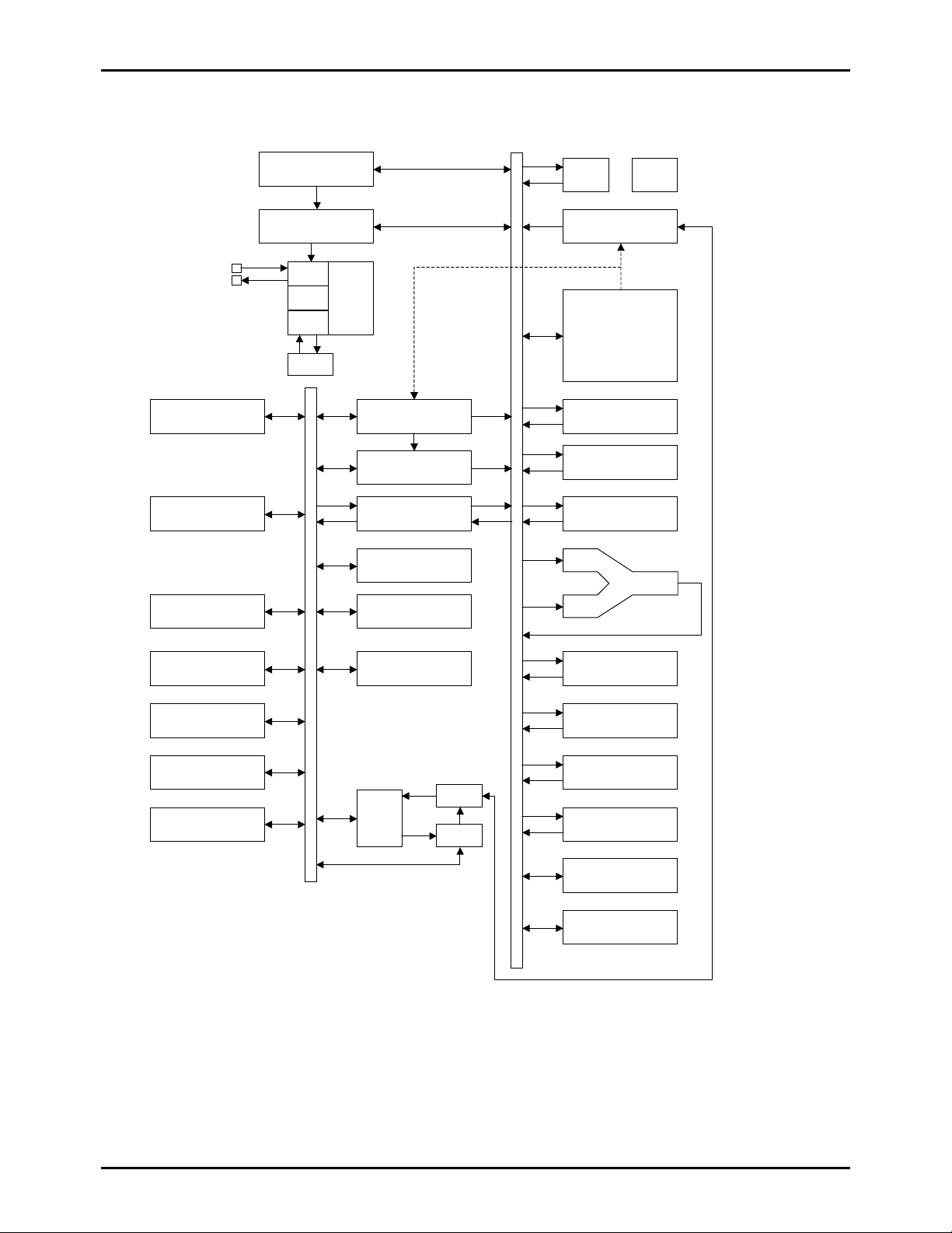
System Bl ock Diagram
IIC
Timer 0
Base Timer
ADC
INT0-3
Noise Rejection Filter
PWM
Data Slicer
Interrupt Control
Standby Control
X’tal
RC
VCO
PLL
LC863432A/28A/24A/20A/16A
Clock
Generator
ROM Correct Control
XRAM
Bus Interface
Port 1
Port 3
Port 7
OSD
Control
Circuit
CGROM
VRAM
IR PLA
ROM
PC
ACC
B Register
C Register
ALU
PSW
RAR
RAM
Stack Pointer
Port 0
Watch Dog Timer
No.6846-5/19
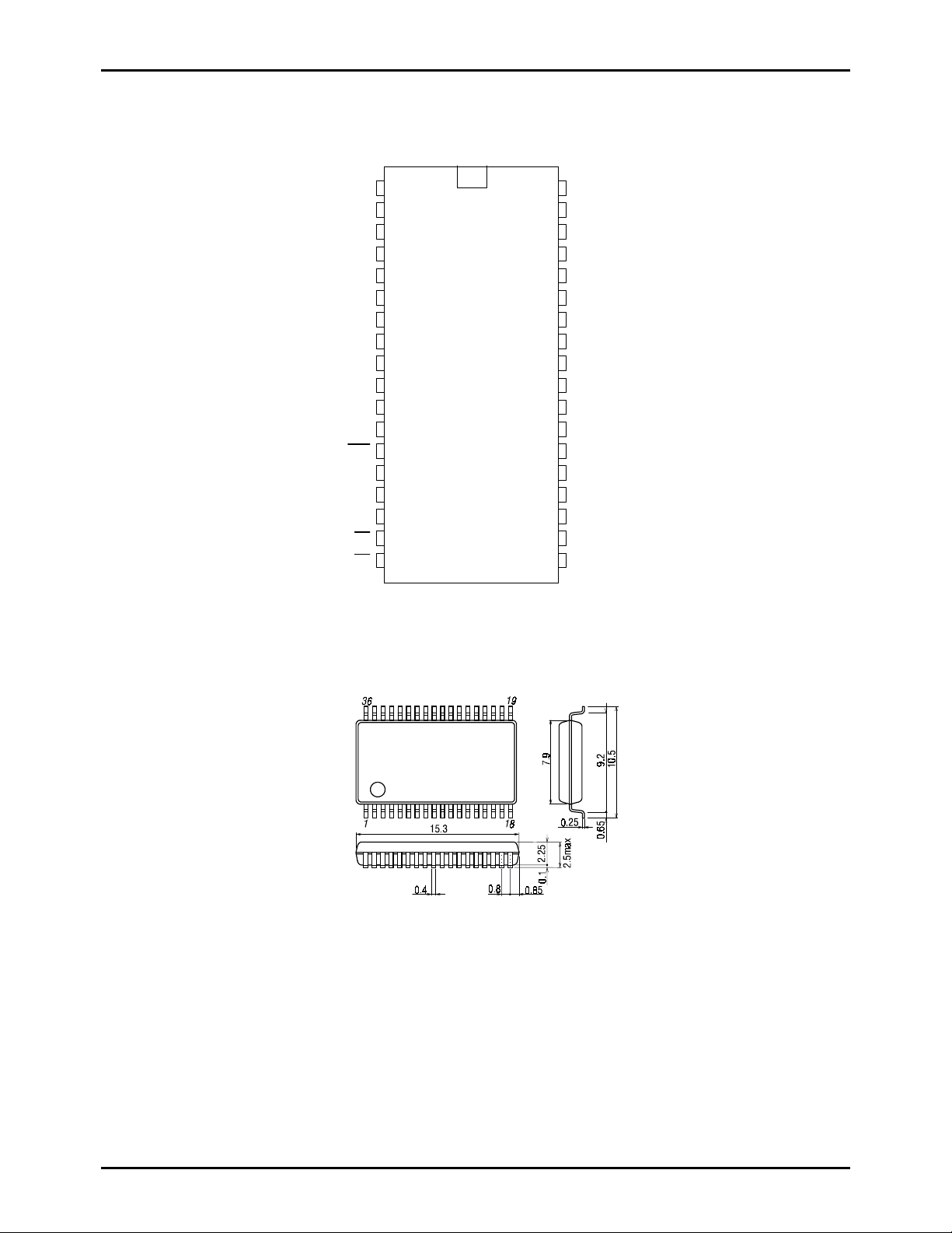
Pin Assignment
Package Dimension
(unit : mm)
3129
P10/SDA0
P11/SCLK0
P12/SDA1
P13/SCLK1
VSS
XT1
XT2
VDD
P04/AN4
P05/AN5
P06/AN6
P07/AN7
RES
FILT
CVIN
P30
VS
HS
LC863432A/28A/24A/20A/16A
1
2
3
4
5
6
7
8
9
10
11
12
13
14
15
16
17
18
36
35
34
33
32
31
30
29
28
27
26
25
24
23
22
21
20
19
P03
P02
P01
P00
P17
P16/PWM3
P15/PWM2
P14/PWM1
P73/INT3/T0IN
P72/INT2/T0IN
P71/INT1
P70/INT0
P32
P31
BL
B
G
R
SANYO : MFP-36S
No.6846-6/19
 Loading...