

Page 1
Ordering number : EN4659
O3098HA (OT)/71093JN B8-0531 No. 4659-1/34
LC85632
SANYO Electric Co.,Ltd. Semiconductor Bussiness Headquarters
TOKYO OFFICE Tokyo Bldg., 1-10, 1 Chome, Ueno, Taito-ku, TOKYO, 110-8534 JAPAN
Digital Alarm Clock
CMOS IC
Any and all SANYO products described or contained herein do not have specifications that can handle
applications that require extremely high levels of reliability, such as life-support systems, aircraft’s
control systems, or other applications whose failure can be reasonably expected to result in serious
physical and/or material damage. Consult with your SANYO representative nearest you before using
any SANYO products described or contained herein in such applications.
SANYO assumes no responsibility for equipment failures that result from using products at values that
exceed, even momentarily, rated values (such as maximum ratings, operating condition ranges, or other
parameters) listed in products specifications of any and all SANYO products described or contained
herein.
Overview
The LC85632 is a multi-function digital clock IC that in
addition to providing current time display supports a
wide range of functions, including an alarm function, a
sleep function, a calendar function, and a function to turn
connected equipment on and off. Furthermore, the
LC85632 provides a simpler user interface than that of
earlier Sanyo products.
Applications
• Alarm clocks
• Clock radios
Functions
• Current time display
• Two independent alarm functions with snooze function
• Sleep timer function (up to 90 minutes)
• Calendar function
One year calendar (January 1 to December 31) that can
display leap year’s day (February 29)
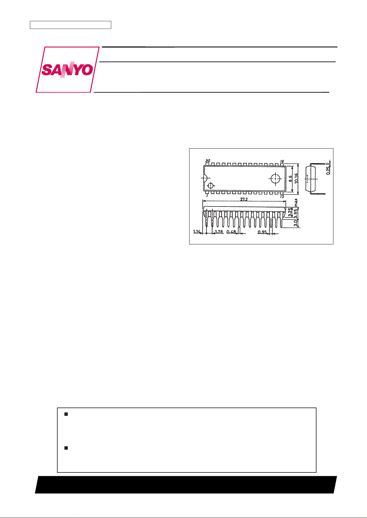
Package Dimensions
unit: mm
3196-DIP30SD
[LC85632]
SANYO: DIP30SD
Page 2
LC85632
No. 4659-2/34
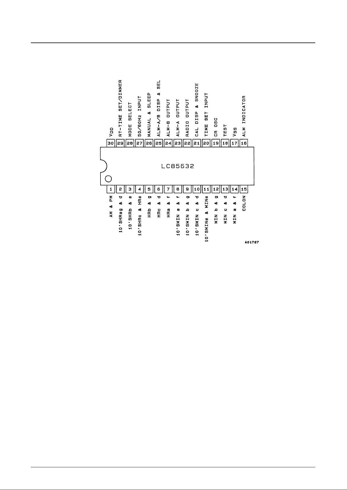
Pin Assignment
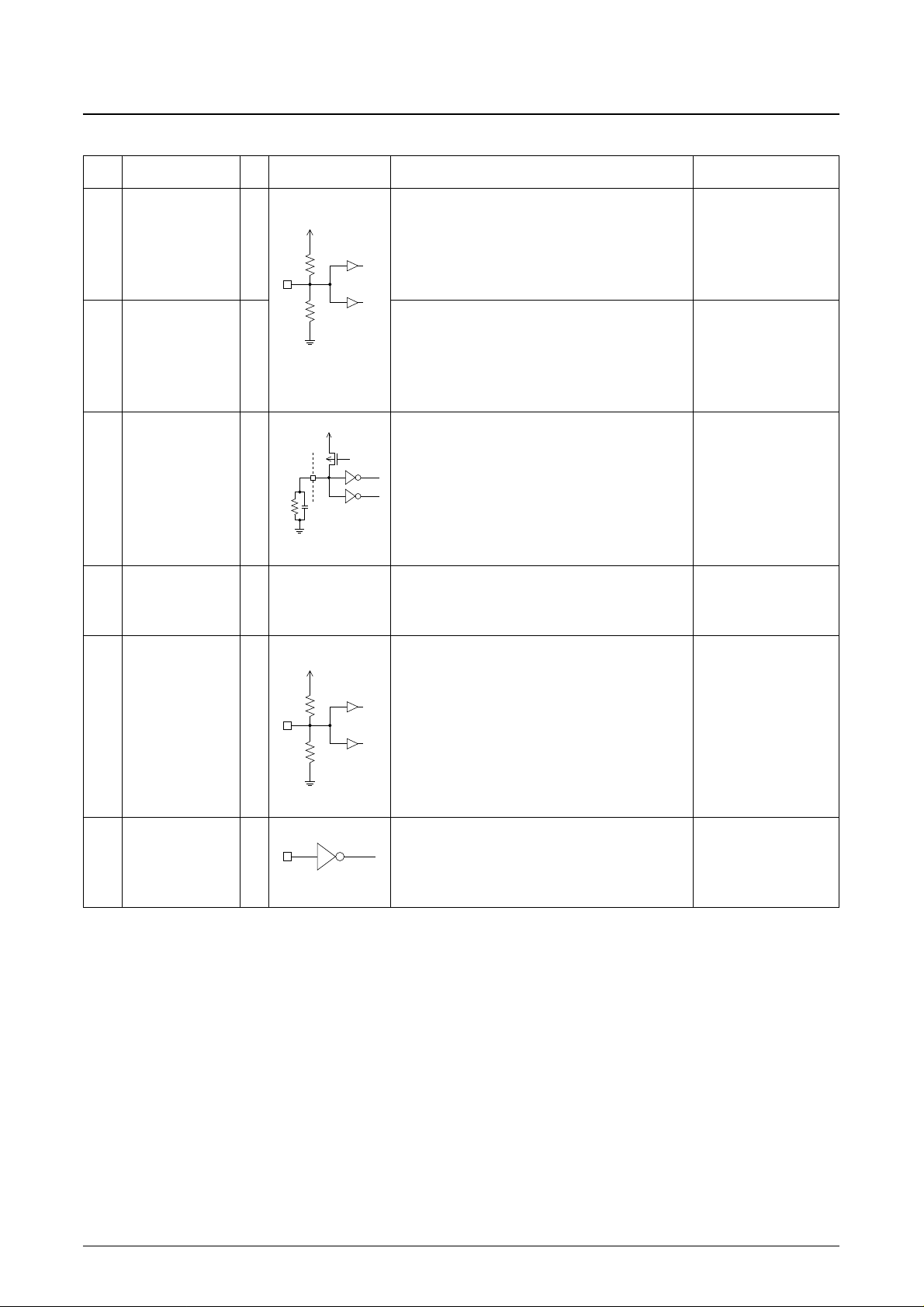
Page 3
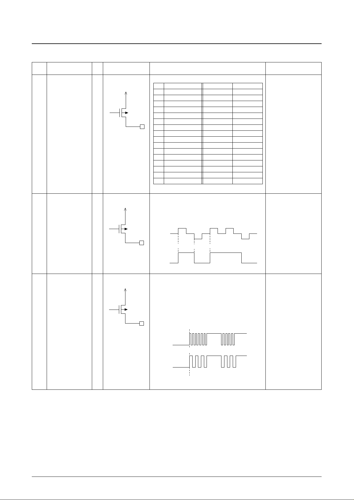
Pin Functions
Internal equivalent
No. Pin I/O
circuit
Pin function Handling when unused
1 AM & PM O LED output pins Open
2 10’SHRag & d O
3 10’SHRb & e O
4 10’SHRc & HRe O
5 HRb & g O
6 HRc & d O
7 HRa & f O
8 10’SMIN a & f O
9 10’SMIN b & g O
10 10’SMIN c & d O
11 10’SMINe & MINe O
12 MIN b & g O
13 MIN c & d O
14 MIN a & f O
15 COLON O
16 ALM INDICATOR O (VDD – 15 V breakdown voltage)
22 RADIO OUTPUT O Outputs a DC voltage. This pin is controlled by the inputs to Open
the MANUAL & SLEEP pin (pin 26). It operates as a toggle.
During normal operation it outputs a low level (high
impedance).
(Normal breakdown voltage)
23 ALM-A OUTPUT O Output alarm signals Open
24 ALM-B OUTPUT O ALM-A OUTPUT: Alarm A
ALM-B OUTPUT: Alarm B
The output waveform is shown below.
During normal operation these pins output a low level
(high impedance).
(Normal breakdown voltage)
Continued on next page.
LC85632
No. 4659-3/34
No. Pin Drive phase 1 Drive phase 2
1 AM & PM AM PM
2 10’SHR ag & d 10’SHR ad 10’SHR g
3 10’SHRb & e 10’SHR e 10’SHR b
4 10’SHRc & HRe HR e 10’SHR c
5 HRb & g HR g HR b
6 HRc & d HR d HR c
7 HRa & f HR f HR a
8 10’SMIN a & f 10’SMIN a 10’SMIN f
9 10’SMIN b & g 10’SMIN b 10’SMIN g
10 10’SMIN c & d 10’SMIN c 10’SMIN d
11 10’SMINe & MINe MIN e 10’SMIN e
12 MIN b & g MIN g MIN b
13 MIN c & d MIN d MIN c
14 MIN a & f MIN f MIN a
15 COLON COLON —
16 ALM INDICATOR ALM-A ALM-B
VDD
VDD
MANUAL & SLEEP pin input level
VDD
OPEN
VSS
RADIO OUT pin output level (when pulled down to VSS)
VDD
VSS
VDD
ALM-A OUTPUT and ALM-B OUTPUT pin output levels
(summary diagram)
* ALM-A OUTPUT (2400 Hz)
VDD
VSS
* ALM-B OUTPUT (1200 Hz)
VDD
VSS
Output start
Page 4
LC85632
Continued from preceding page.
Internal equivalent
No. Pin I/O
circuit
Pin function Handling when unused
20 TIME SET INPUT 3I Input pin that starts the setting/update of the current time, Open
the alarm time, or the calendar date. Normally left open
(NOP).
The application of a high level is taken as a + input,
which increases the value of the setting, and a low is taken
as a – input, which decreases the value of the setting.
21 CAL DISP & 3I Input pin for calendar display and snooze. Open
SNOOZE
Normally left open. When a high level is applied the
calendar displays the day and month, and when a low level
is applied the calendar displays the month and day.
However, if an alarm signal is being output from either
ALM-A OUTPUT or ALM-B OUTPUT (pin 23 or 24) the
calendar is not displayed, but rather a snooze operation is
started.
25 ALM-A/B DISP & SEL 3I Input pin for switching between alarm mode and current Open
time mode. Normally left open. When a high level is applied,
the current time setting for alarm A is displayed, and when
a low level is applied, the current time setting for alarm B is
displayed. In either case, the time setting and the operation
enable/disable state can be changed.
26 MANUAL & SLEEP 3I Input pin for setting the RADIO OUTPUT pin (pin 22) output Open
control and the sleep function time. Normally left open.
When a high level is applied the RADIO OUTPUT goes
high. This pin can also be used for setting the sleep
function time. When a low level is applied the RADIO
OUTPUT goes low. When either a low level or a high level
is applied, any alarm output in progress will be stopped.
Continued on next page.
No. 4659-4/34
VDD
H
L
H:L:High threshold
input
Low threshold
input
VDD
H
L
H:L:High threshold
input
Low threshold
input
Page 5
Continued from preceding page.
Internal equivalent
No. Pin I/O
circuit
Pin function Handling when unused
28 MODE SELECT 3I Input pin for switching the operating mode. Either left open, connected
Switches the display mode and the clock input to the to VDD, or connected to
50/60 Hz INPUT pin (pin 27). ground.
High: 50 Hz/24 hour display
Open: 60 Hz/12 hour display
Low: 50 Hz/12 hour display
29 RT-TIME 3I Input pin for switching the enabled/disabled state for setting Open
SET/DIMMER the time.
Normally left open.
High: Current time display/current time setting mode
Open: Current time display/current time setting disabled
Low: Dimmed display/current time setting disabled
19 CR OSC I/O Connection pin for external RC circuit. Connected to VDD
An oscillator circuit with a frequency of 4800 Hz can be
formed using the following R and C values.
R = 68 kΩ
C = 4700 pF
17 VSS I — Power supply pins. —
30 VDD I VSS = 0 V
VDD = +5 V (standard)
18 TEST 3I LSI test pin. Open
Normally left open.
27 50/60 Hz INPUT I Input pin for the 50/60 Hz input for the clock.
(Schmitt input)
Note: •
“3I” is an abbreviation for “three value input pin.” The inputs to these pins can be either high, open, or low. These pins are left open during normal use.
• NOP: “No operation”
LC85632
No. 4659-5/34
VDD
H
L
H:L:High threshold
input
Low threshold
input
VDD
External RC
constant circuit
VDD
H:L:High threshold
input
Low threshold
input
H
L
Page 6
LC85632
Three Value Input Circuits: H: High level, M: Open, L: Low level, NOP: No operation
• MODE SELECT
Input level Mode
H 50 Hz/24 hour display
M 60 Hz/12 hour display
L 50 Hz/12 hour display
• TIME SET INPUT
Input level Mode
H Up
M NOP
L Down
• RE-TIME SET/DIMMER
Input level Mode
H Current time display/current time setting mode
M Current time display/NOP
L Dimmed display/NOP
• CAL DISP & SNOOZE
Input level Mode
H Calendar display (day·month)/calendar setting/snooze on
M Current time display/NOP
L Calendar display (month·day)/calendar setting/snooze on
• ALM-A/B DISP & SEL
Input level Mode
H Alarm A setting display/setting
M Current time display/NOP
L Alarm B setting display/setting
• MANUAL & SLEEP
Input level Mode
H ON input/sleep-in
M Current time display/NOP
L OFF input
• TEST
Input level Mode
H Illegal setting
M Normal operation
L LED test
No. 4659-6/34
Page 7
Specifications
Absolute Maximum Ratings at Ta = 25°C, VSS= 0 V
Parameter Symbol Applicable pin Conditions Ratings Unit
Maximum power supply voltage V
DD
max –0.3 to +7.0 V
Input voltage V
IN
(1) All input pins other than the –0.3 to VDD+ 0.3 V
50/60 Hz INPUT pin
VIN(2) 50/60 Hz INPUT Pin voltage –0.3 to VDD+ 0.3
With a 100 kΩ currentlimiting V
DD
– 12 to VDD+ 12
resistor inserted in the input, at
that resistor’s terminal.
Input clamping current I
IN
50/60 Hz INPUT With a 100 kΩ limiting resistor –0.4 to +0.4 mA
inserted in the input.
Output voltage V
OUT
(1) CR OSC –0.3 to VDD+ 0.3 V
Output voltage V
OUT
(2) RADIO OUTPUT –0.3 to VDD+ 0.3 V
ALM-A OUTPUT
ALM-B OUTPUT
Output voltage V
OUT
(3) LED SEGMENT output pins VDD– 15 to VDD+ 0.3 V
(pins 1 to 16)
Total output current ∑I
LED
Total for the LED The average value of the –280 to 0 mA
SEGMENT output pins effective current value within
(pins 1 to 16) a single display cycle
according to the 50 or 60 Hz
frequency.
Maximum power dissipation Pdmax Ta = –30 to +70°C 700 mW
Ambient temperature: operating Topr –30 to +70 °C
Ambient temperature: storage Tstg –55 to +125 °C
Allowable Operating Ranges at Ta = –30 to +70°C, VSS= 0 V
Ratings
Parameter Symbol Applicable pin Conditions
min typ max
Unit
Operating power supply voltage V
DD
4.0 5.0 6.0 V
Input high level voltage V
IH
(1) CR OSC 0.75 V
DD
V
DD
V
Input low level voltage V
IL
(1) V
SS
0.25 V
DD
V
Input high level voltage V
IH
(2) TIME SET INPUT The intermediate is the VDD– 0.5 V
DD
V
CAL DISP & SNOOZE open pin state.
Input intermediate level voltage VIM(2)
ALM-A/B DISP & SEL The rated values apply
1/2 VDD– 0.5 1/2 VDD+ 0.5 V
MANUAL & SLEEP when an external signal
MODE SELECT is applied.
Input low level voltage V
IL
(2)
RT-TIME SET/DIMMER
V
SS
VSS+ 0.5 V
TEST
Input high level voltage V
IH
(3) 50/60 Hz INPUT VDD– 0.5 VDD+ 0.3 V
Input low level voltage V
IL
(3) V
SS
VDD– 3.0 V
Operating frequency fOP 50/60 Hz INPUT 1 2000 Hz
Input level hold time tH All three value input pins 10 ms
Input chattering time tC All three value input pins 10 ms
LC85632
No. 4659-7/34
Page 8
LC85632
Electrical Characteristics at Ta = 25°C, VDD= 5 V, VSS= 0 V
Ratings
Parameter Symbol Applicable pin Conditions
min typ max
Unit
Output high level current I
OH
(1) 10’ SHRag & d Output on, (Note 1) –32 mA
V
OUT
= VDD– 2.0 V
Output off leakage current I
OF
(1) Output off, –20 µA
V
OUT
= VDD– 12 V
Output high level current I
OH
(2) AM & PM Output on, (Note 2) –16 mA
10’SHRb & e V
OUT
= VDD– 2.0 V
10’SHRc & HRe
HRb & g
HRc & d
HRa & f
10’SMIN a & f
10’SMIN b & g
10’SMIN c & d
10’SMINe & MINe
MIN b & g
MIN c & d
MIN a & f
Output off leakage current I
OF
(2) COLON Output off, –20 µA
ALM INDICATOR V
OUT
= VDD– 12 V
Output high level current I
OH
(3) RADIO OUTPUT Output on, –2 mA
ALM-A OUTPUT V
OUT
= VDD– 2.0 V
Output off leakage current I
OF
(3)
ALM-B OUTPUT
Output off, –10 µA
V
OUT
= V
SS
Input high level current IIH(2) CR OSC VIN= V
DD
10 µA
Input low level current I
IL
(2) VIN= V
SS
–2 mA
Input high level current I
IH
(3) TIME SET INPUT VIN= V
DD
10 100 µA
CAL DISP & SNOOZE
ALM-A/B DISP & SEL
Input low level current I
IL
(3)
MANUAL & SLEEP
VIN= V
SS
–100 –10 µA
MODE SELECT
RT-TIME SET/DIMMER
TEST
Pull-up resistance R
PU
TIME SET INPUT VIN= 1/2 V
DD
1.0 MΩ
CAL DISP & SNOOZE
ALM-A/B DISP & SEL
Pull-down resistance R
PD
MANUAL & SLEEP
0.8 MΩ
MODE SELECT
RT-TIME SET/DIMMER
TEST
Oscillator stability fS CR OSC (Note 2) V
DD
= 5.0 V –10 +10 %
Oscillator precision fA CR OSC (Note 2) V
DD
= 5.0 V –10 +10 %
Oscillator frequency f
OSC
CR OSC R = 91 kΩ ±1% 4800 Hz
C = 3300 pF ±5%
Initial reset power supply voltage V
DET
V
DD
Power supply voltage 2.5 4.0 V
V
SS
range when initial reset
operates.
Current dissipation (operating) I
DD
With no output load 2 mA
Note: 1. In addition to not exceeding the total output current
ΣILED (from the absolute maximum ratings table), the segment output currents are allowed the
following values within a 700 mW total power dissipation range.
10’SHRag & d: Up to –78 mA
Others: Up to –39 mA
Current flowing out of the IC is expressed with negative values, and current flowing into the IC is expressed with positive values.
2. The total variation in the oscillator frequency will be the sum of the precision and the stability. That is, the limiting values for the oscillator frequency
variation fall within the range from fosc - 19% to fosc + 21%.
No. 4659-8/34
Page 9
Functional Description
Segment Output
This IC can directly drive with its 16 segment pins duplex type LED panels that include colon and alarm indicators.
However, since the total value of the LED drive current (∑ILED) flowing into the LED panel is limited to its absolute
maximum value, caution is required in design.
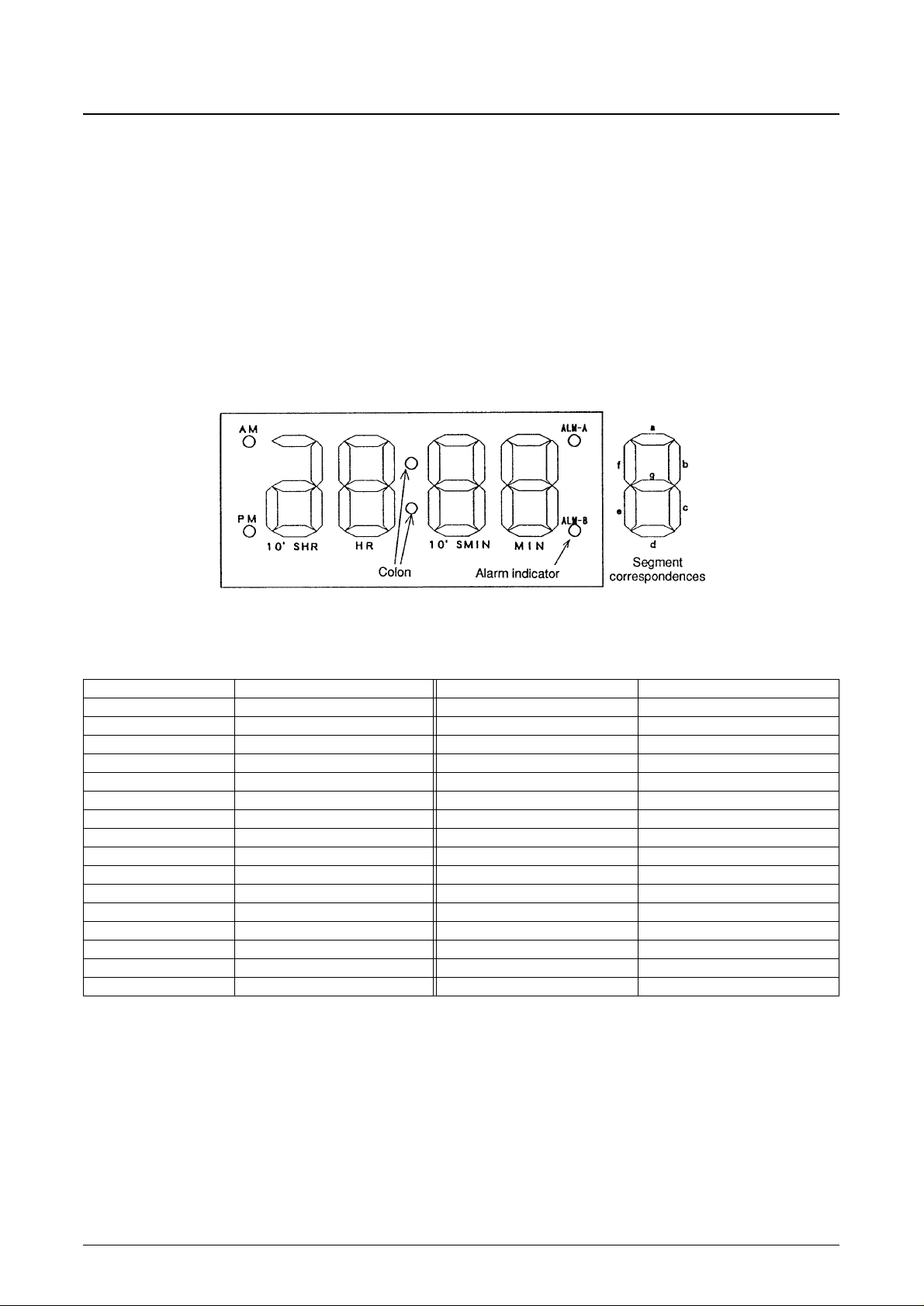
Figure 1 shows the correspondence between the LC85632 segment outputs and the LED panel. For example, pin 2 (the
10’SHRag & d pin) drives the segments ‘a’, ‘g’, and ‘d’ in the 10’SHR digit. Table 1 shows the correspondence between
the drive phases and the segments that light.
Note that figure 1 is a generalized LED panel and not an exact representation of any particular product.
Figure 1 LED Panel and LED Segments
Table 1 Segment Lighting Correspondences for the Drive Phases
No. Pin Drive phase 1 Drive phase 2
1 AM & PM AM PM
2 10’SHRag & d 10’SHR ad 10’SHR g
3 10’SHRb & e 10’SHR e 10’SHR b
4 10’SHRc & HRe HR e 10’SHR c
5 HRb & g HR g HR b
6 HRc & d HR d HR c
7 HRa & f HR f HR a
8 10’SMIN a & f 10’SMIN a 10’SMIN f
9 10’SMIN b & g 10’SMIN b 10’SMIN g
10 10’SMIN c & d 10’SMIN c 10’SMIN d
11 10’SMINe & MINe MIN e 10’SMIN e
12 MIN b & g MIN g MIN b
13 MIN c & d MIN d MIN c
14 MIN a & f MIN f MIN a
15 COLON COLON —
16 ALM INDICATOR ALM-A ALM-B
LC85632
No. 4659-9/34
Page 10
LC85632
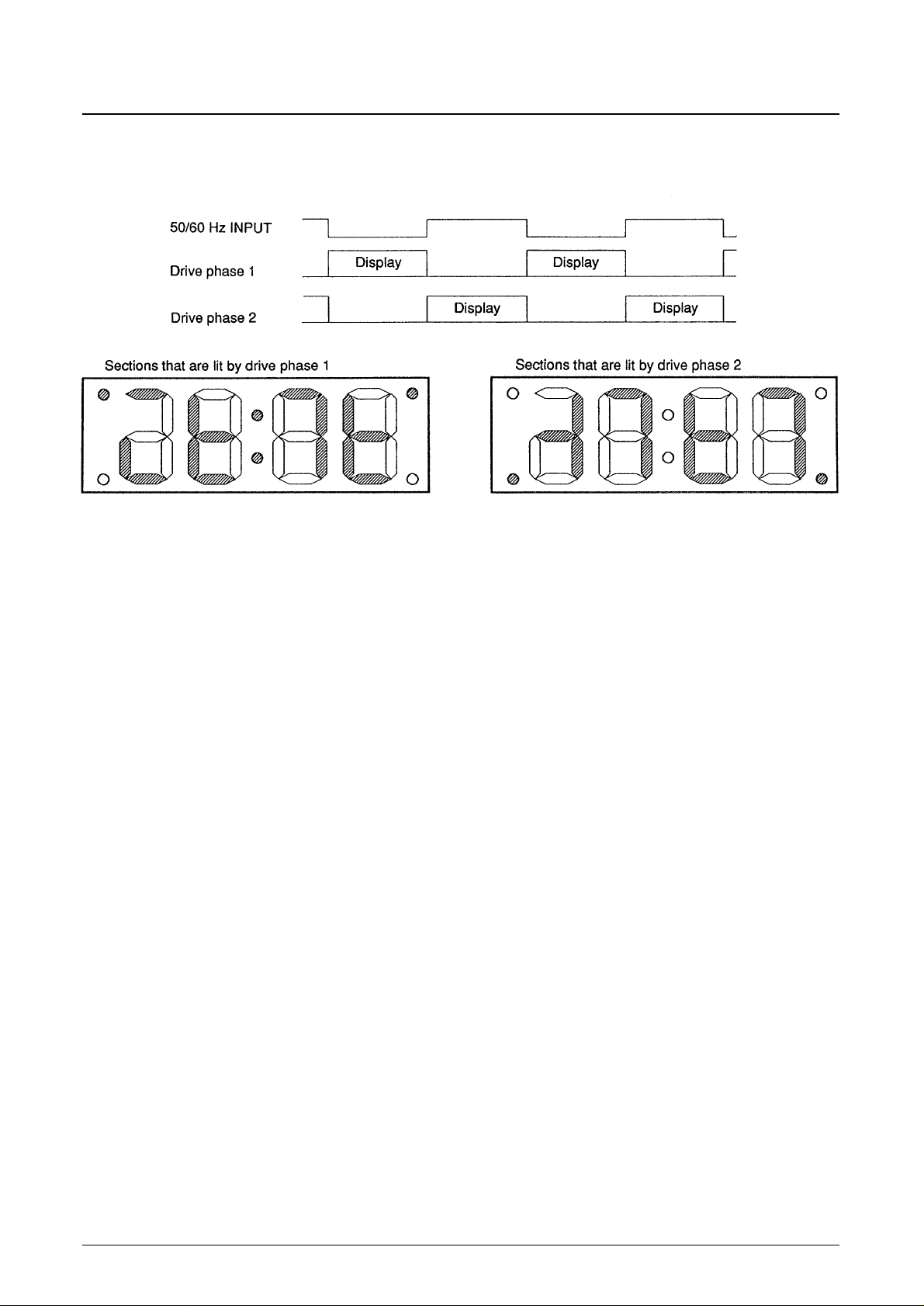
Figure 2 shows the sections where LEDs are lit for each drive phase. This figure is based on the generalized drawing
shown in figure 1, and the shaded sections show the segments that are lit by the corresponding phase.
Figure 2 LED Sections Lit by the Drive Phases
No. 4659-10/34
Page 11
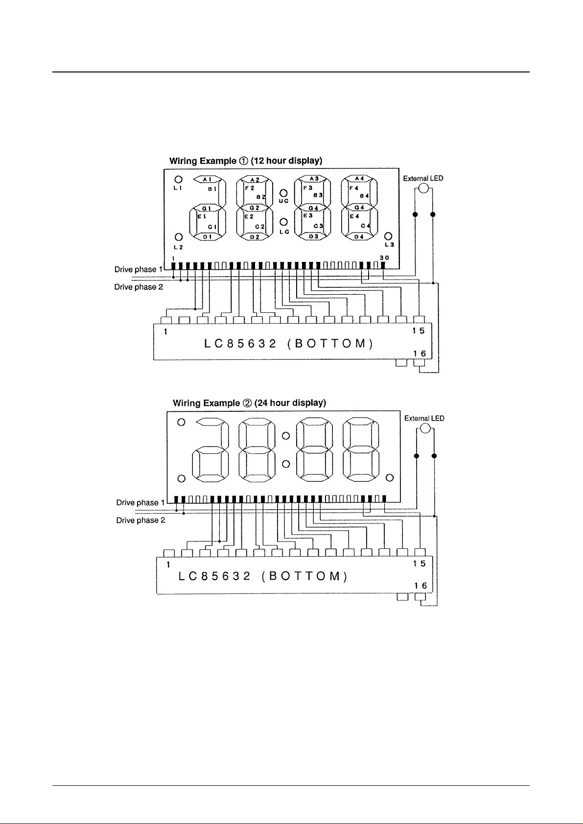
Figure 3 shows actual wiring examples for 12 hour and 24 hour displays for the Tottori Sanyo, Ltd., SL-1042-30T LED
panel. However, since the SL-1042-30T LED panel does not have an alarm A display LED, an external LED is used for
alarm A display. Also, the calendar day/month display cannot be used with this circuit.
Figure 3 LED Panel Wiring Examples
LC85632
No. 4659-11/34
Page 12

LC85632
The following figures show the circuit diagrams for LED panels that can also display the alarm and calendar functions.
These panels are the SL-1994-54T (for 12 hour display) and the SL-1994-55T (for 24 hour display), and are both made
by Tottori Sanyo, Ltd.
The calendar day/month cannot be used with this circuit.
Figure 4 Wiring and Connection Example Using the SL-1994-54T LED Panel (12 hour display)
Figure 5 Wiring and Connection Example Using the SL-1994-55T LED Panel (24 hour display)
No. 4659-12/34
Page 13

Oscillator Circuit
A 4800 Hz oscillator can be constructed by connecting a resistor and a capacitor to the CR OSC pin (pin 19). This
oscillator is used as the internal clock for detecting the loss of external power, for alarm tones, and for the dimmer duty
cycle. Therefore, it operates continuously during normal operation. In this section, we describe the operation when the
AC input to the 50/60 Hz INPUT pin falls below 1 Hz.
During a power outage, LED segment output from pins 1 to 16 is stopped. Also when power is restored and the AC input
becomes over 1 Hz, the whole LED display (except for the alarm indicator) flashes. The period of this flashing is 1 Hz.
This period is created by dividing the period of the AC input from the 50/60 Hz either by 50 when the clock is operated
at 50 Hz, i.e., when either a low or high level is applied to the MODE SELECT pin, or by 60 when the clock is operated
at 60 Hz, i.e., when the MODE SELECT pin is left open. Apply either a high level or a low level to the TIME SET
INPUT pin to stop the flashing. In either case the flashing will stop and the chip will return to normal operation, i.e.,
current time display.
Tie the CR OSC pin high if the oscillator circuit is not used. In this case the IC will not detect power loss. Also, the
alarm function will not operate correctly, but will output either no signal or an irregular signal. Furthermore, no segment
signals will be output in dimmer mode.
Note that if an oscillator circuit is not used, the high level applied to the CR OSC pin must be applied before power is
applied. If the oscillator is forcibly stopped by applying a high level in the state where the CR oscillator is operating after
power has been applied the alarm DC output may operate incorrectly.
Dual Alarms
This IC provides two 24-hour alarms systems, each of which can be set in 1 minute increments. Alarm A outputs a
2400 Hz alarm tone, and alarm B a 1200 Hz tone. (See the “Alarm” section for details on the alarm waveforms.) The
alarm tones are output continuously for 59 minutes, but can be interrupted for 6 to 7 minutes by the snooze function.
Calendar
This IC includes an on-chip full-year month and day display calendar function. The display can be switched to be either
a month/day or a day/month format. The calendar function can be set to display leap year’s day (February 29) on what
would have been March 1 by applying a low level to the TIME SET INPUT pin.
Sleep Function
This IC includes a 90 minute sleep circuit (off timer) that can be set easily. The sleep function time setting can be set to
be 90, 60 , 45, 30, or 15 minutes in an “easy set” format.
LC85632
No. 4659-13/34
Page 14

LC85632
Operating State Transition Diagram
Figure 6 Operating State Transitions 1: Overall
No. 4659-14/34
Page 15

Figure 7 Operating State Transitions 2: Current Time Display and Setting Block
LC85632
No. 4659-15/34
Power on
State
Display
Initial state
①
Current time, flashing
12 00 (Phase
①
)
: (Phase
②
)
—
Numbers
Colon
ALM IND
AM/PM
ALARM
SLEEP
SNOOZE
Operation
Note:
Depends on the display
mode
The clock operates even in
this state.
Normal clock
Not set
Not set
Not set
To the alarm display and setting blockTo the calendar and snooze block To the manual and sleep block
Application of a
high or low level
to the ALM-A/B
DISP & SEL pin.
Application of a
high or low level
to the CAL DISP
& SNOOZE pin.
Application of a
high or low level
to the MANUAL
& SLEEP pin.
State
Display
Normal display
Current time
Current time
Lit
—
Numbers
Colon
ALM IND
AM/PM
ALARM
SLEEP
SNOOZE
Operation
Note:
Depends on the display
mode
The TIME SET INPUT is a
NOP in this mode.
Normal clock
No change
No change
No change
State
Display
Normal state
Current time
Current time
Lit
Lit*
—
Normal clock
Set
Not set
Not set
Numbers
Colon
ALM IND
AM/PM
ALARM
SLEEP
SNOOZE
Operation
Note: *
The indicators for
enabled alarms are lit.
Display
Current time
Colon
ALM IND
AM/PM
ALARM
SLEEP
SNOOZE
Operation
Note:
Depends on the
display mode
No change
No change
No change
When alarm operation is not enabled
When alarm operation is enabled
Linked to the + and
– inputs
Linked to the + and
– inputs
Flashing
Lit for enabled alarms
Current time setting
mode
State
Numbers
Application of a high level
to the RT-TIME SET/
DIMMER pin.
Making the RT-TIME SET/
DIMMER pin open.
Display
Current time
Colon
ALM IND
AM/PM
ALARM
SLEEP
SNOOZE
Operation
Note:
Depends on the
display mode
No change
No change
No change
Linked to the + and
– inputs
Linked to the + and
– inputs
Flashing
Lit for enabled alarms
Current time setting
mode
State
Numbers
Alarm operation starts at
the point the time matches
an alarm setting time.
Application of a high level
to the RT-TIME SET/
DIMMER pin.
Making the RT-TIME SET/
DIMMER pin open.
Note: The “Display” sections indicates the states of the LED display.
Abbreviations: ALM IND. ➝ Alarm indicator, AM/PM ➝ AM, PM
Application of a high level to the
RT-TIME SET/DIMMER pin.
Application of a high or low level to
the TIME SET INPUT pin.
Page 16

LC85632
Figure 8 Operating State Transitions 3: Alarm Display and Setting Block
No. 4659-16/34
From initial state
①
From the current time display and setting block
To the current time display and setting block
Application of a
high or low level
to the TIME SET
INPUT pin.
The following are the alarm stop conditions during output.
• An OFF input (pin 22 = VSS)
• An ON input (pin 22 = VDD)
• Arrival at the point 59 minutes following start of alarm output.
• A snooze input (pin 21 = VDD or VSS) (Alarm output restarts after the completion
of the snooze operation.)
• The start of another alarm operation during alarm operation.
State
Display
Initial state
②
Alarm
12 00
Flashing
Either A or B flashing
Numbers
Colon
ALM IND
AM/PM
ALARM
SLEEP
SNOOZE
Operation
Note:
If the current time display is
flashing, that flashing is
stopped.
Application of a high or
low level to the ALM-A/B
DISP & SEL pin, thus
selecting the alarm display
and setting mode.
Application of a high or
low level to the ALM-A/B
DISP & SEL pin, thus
selecting the alarm display
and setting mode.
Clearing alarm display
and setting mode.
(Making the ALM-A/B
DISP & SEL pin open.)
Operation enabled
—
—
Depends on the
display mode
State
Display
Alarm time setting
Alarm
Set time display
Flashing
Either A or B flashing
Numbers
Colon
ALM IND
AM/PM
ALARM
SLEEP
SNOOZE
Operation
Note:
Operation enabled
—
—
Depends on the
display mode
Alarm setting time
display
State
Display
Alarm operation disable
Alarm
Set time display
Flashing
Enabled alarm flashing
Numbers
Colon
ALM IND
AM/PM
ALARM
SLEEP
SNOOZE
Operation
Note:
In the alarm not set mode, the
alarm will not operate even if
the set time is the same as the
current time.
Operation enabled
—
—
Depends on the
display mode
Alarm setting time
display
Display
Alarm
Colon
ALM IND
AM/PM
ALARM
SLEEP
SNOOZE
Operation
Note:
Depends on the
display mode
Operation enabled
—
—
Linked to the + and
– inputs
Linked to the + and
– inputs
Flashing
Either A or B flashing
Alarm time setting
State
Numbers
Alarm output starts if the
current time matches the
setting time.
Making the TIME
SET INPUT pin
open.
Application of a low
level to the MANUAL/
SLEEP pin.
Application of a
high or low level
to the TIME SET
INPUT pin.
Page 17

Figure 9 Operating State Transitions 4: Calendar Display and Setting Block
LC85632
No. 4659-17/34
From initial state
①
From the current time display and setting block
To the current time display and setting block
Application of a
high or low level
to the TIME SET
INPUT pin.
State
Display
Initial state
③
Calendar
1 1
Off
Enabled alarms lit
Off
Normal clock
No change
No change
No change
Numbers
Colon
ALM IND
AM/PM
ALARM
SLEEP
SNOOZE
Operation
Note:
Application of a high or
low level to the CAL DISP
& SNOOZE pin in the
initial state (1) state, thus
displaying the calendar.
Application of a high
or low level to the CAL
DISP & SNOOZE pin in
a state in which no alarm
signal is being output.
Display
Calendar
Colon
ALM IND
AM/PM
ALARM
SLEEP
SNOOZE
Operation
Note:
Linked to the + and
– inputs.
Off
Enabled alarms lit
Off
Normal clock
No change
No change
No change
Calendar settingState
Numbers
When backing up the calendar
the date (display) changes from
3/1 to 2/29, and then to 2/28.
Making the TIME
SET INPUT pin
open.
Application of a
high or low level
to the TIME SET
INPUT pin.
Making the CAL
DISP & SNOOZE
pin open.
State
Display
Calendar display
Calendar
Current date
Off
Enabled alarms lit
Off
Normal clock
No change
No change
No change
Numbers
Colon
ALM IND
AM/PM
ALARM
SLEEP
SNOOZE
Operation
Note:
Page 18

LC85632
Figure 10 Operating State Transitions 5: Manual and Sleep Block
No. 4659-18/34
Current time display and setting block
(From initial state
①
)
Was
there an ON
input?
Turn on the display and
set the RADIO OUTPUT
pin high.
ON state
Sleep setting
Have 2
seconds passed
since the
input?
Was
there an ON
input?
Reset the sleep count
to 90 minutes.
Have 2
seconds passed
since the
input?
Was
there an ON
input?
To the current time display and
setting block
Start the sleep count
Reset the sleep count
to 60 minutes.
Have 2
seconds passed
since the
input?
Was
there an ON
input?
Reset the sleep count
to 45 minutes.
Have 2
seconds passed
since the
input?
Was
there an ON
input?
Reset the sleep count
to 30 minutes.
Have 2
seconds passed
since the
input?
Was
there an ON
input?
Reset the sleep count
to 15 minutes.
Have 2
seconds passed
since the
input?
Was
there an ON
input?
Restore the display to
normal display.
Set the RADIO OUTPUT pin
to the low level.
Have 2
seconds passed
since the
input?
Was
there an ON
input?
* To A
* A
State
Display
ON state
“On” display
—
Off
Enabled alarms lit
Off
ON operation
No change
—
—
Numbers
Colon
ALM IND
AM/PM
ALARM
SLEEP
SNOOZE
Operation
Note:
The RADIO OUTPUT pin
is set to the high level.
State
Display
Sleep set
Set tie display
Sleep setting time
Off
Enabled alarms lit
Off
Linked to “ON” inputs
No change
Count starts
—
Numbers
Colon
ALM IND
AM/PM
ALARM
SLEEP
SNOOZE
Operation
Note:
The sleep setting time is
changed according to
“ON” inputs.
** “ON input”: The application of a high level to the MANUAL & SLEEP pin.
When the RADIO OUTPUT pin output is at the high level, the OFF input
(application of a low level to the MANUAL & SLEEP pin) will always be valid.
(If the RADIO OUTPUT pin is at the low level, the sleep counter will be reset
and the count stopped.)
No
Yes
Yes
No
Yes
No
Yes
No
No
Yes
No
Yes
Yes
No
Yes
No
No
Yes
Yes
No
No
Yes
Yes
No
No
Yes
Yes
No
No
Yes
Page 19

Operation
Clearing the Initial Reset State
In the initial state when power is first applied, the display reads 12:00 (or 0:00 for 24 hour display) and the numbers and
the colon flash alternately. This is called the “initial reset state”. The period of the flashing is 1 Hz.
To clear the flashing state, apply a high or low level to the TIME SET INPUT pin when the colon is lit.
Figure 11 Clearing the Initial Input State Flashing
In figure 11, the shaded areas under the LED display line are times when the numbers are lit. At these times the colon
will be off.
Here, the application of an input to the TIME SET INPUT input ① in the figure when the numbers are lit, i.e., the timing
indicated by “A”, will be invalid. Since the colon is off at that point, the flashing state will not be cleared. However, such
an input is valid at a point when the numbers are off, i.e., the timing indicated by “B”. Since the colon will be lit in this
state, the flashing state will be cleared and the clock will enter normal display mode.
Alternatively, an input signal such as the TIME SET INPUT input ② in the figure can be applied. Here, the low (or high)
level is held until the flashing is cleared at the timing indicated by “D” in the figure.
When the flashing state is cleared, the colon also will stop flashing, and remain lit.
LC85632
No. 4659-19/34
Page 20

LC85632
Setting the Time
* RT-TIME SET/DIMMER [Pin 29]
VSS OPEN VDD
DIMMER NOP Current time setting mode
(1/4 DUTY) (Current time display)
* TIME SET INPUT [Pin 20]
VSS OPEN VDD
DOWN NOP UP
(Back) (Current time display) (Forward)
(1) Normal operation (current time display mode)
RT-TIME SET/DIMMER pin: Open
TIME SET INPUT pin: Open
In this state the current time is displayed and inputs to the TIME SET INPUT pin (pin 20) for setting the time will be
ignored.
(2) Current time setting mode
The IC can be switched to the current time setting mode by applying a high level to the RT-TIME SET/DIMMER
pin (pin 29). The current time can only be changed in this mode, and is changed by inputs to the TIME SET INPUT
pin (pin 20). The current time setting mode and the current time display mode can be distinguished by the state of the
colon. If the colon is lit steadily then the IC is in display mode, and if the colon is flashing with a 1 Hz period then
the IC is in setting mode. Normally, the clock continues to operate in setting mode.
If a high level is applied to the TIME SET INPUT pin in setting mode, the second counter is reset to zero and the
time is advanced by one minute. Inversely, if a low level is applied, the second counter is reset to zero and the time is
backed up by one minute. In either case, clock operation is interrupted at the point that the input is applied to the
TIME SET INPUT pin. Furthermore, if the input is held for over 0.5 to 1.0 seconds, the IC switches to quick forward
(or quick reverse) mode. In these modes, counting speed will be 20 msec/count for a 50 Hz input to the 50/60 Hz
INPUT pin, and 17 msec/count for a 60 Hz input to that pin.
When the time has been set, normal clock operation can be restarted by making the TIME SET INPUT pin open.
(3) Dimmer display
RT-TIME SET/DIMMER pin: Low level
If an RC circuit is connected to the CR OSC pin (pin 19) this input can be used to set the LED lit time to 1/4 of that
in normal operation, thus reducing the effective LED brightness. This sets the LED display to a 1/4 duty cycle. In
this mode, the LED on time will 1/4 of that in normal operation, with no influence on any other operation.
If an RC circuit is not provided the LED output will go to zero, i.e., this input can be used to turn off LED display.
This operation is a toggle operation. The first time a low level is applied to the RT-TIME SET/DIMMER pin
dimmed display is setup, and the next time a low level is applied the display will return to normal.
No. 4659-20/34
Page 21

Alarm
* ALM-A/B DISP & SEL. [Pin 25]
V
SS
OPEN V
DD
Alarm B set time display NOP Alarm A set time display
(Setting enabled) (Current time display) (Setting enabled)
(1) Entering alarm mode
Alarm A set time display (setting enabled): High level
Alarm B set time display (setting enabled): Low level
This pin should be left open in normal operation.
Applying a high or low level to this pin displays the set time for alarm A (high level) or alarm B (low level) and
enables the alarm time to be set. The display switches to set time display (with an initial value of 12:00 or 0:00) and
the colon and the corresponding alarm indicator (ALM INDICATOR) flash in synchronization.
(2) Adjusting the set time
The alarm time settings are adjusted by displaying the alarm whose setting is to be changed, and then inputting a
high or low level to the TIME SET INPUT pin (pin 20). We will refer to these latter operations as “+ input” and “–
input” in the remainder of this section.
The initial value of the display will be 12:00 (or 0:00) unless there was a previous setting, in which case that value is
displayed. The alarms are set in 1 minute increments, and the setting is changed by one minute each time a + input or
a – input is applied. Furthermore, if the + or – input is applied for more than 0.5 to 1.0 seconds the setting changes at
a speed of 20 msec per increment when 60 Hz is input to the 50/60 Hz INPUT pin, and at 17 msec per increment for
a 50 Hz input. Note that alarm output will start if the set time and the current time match during alarm setting.
(3) Enabling and disabling alarms
Use the following methods to enable and disable the alarms.
• Enabling an alarm
At the point that the set time for the alarm to be operated is displayed, that alarm is enabled, and the alarm
indicator (ALM INDICATOR) for that alarm is displayed.
• Disabling an alarm
When an alarms time setting is displayed, that alarm can be disabled by applying a low level to the MANUAL pin.
At this point the colon will blink continuously and the alarm indicator for the corresponding alarm will go out.
Note that the set time is maintained, i.e., is not reset.
(4) Alarm operating conditions
The alarm operates under either of the following conditions:
• If the alarm set time and the current time agree when alarm operation is enabled.
• If the alarm set time and the current time agree while setting the alarm time, i.e., while advancing or backing up the
alarm time setting.
(5) Alarm operation termination conditions
Alarm output stops if any of the following conditions are met.
• If a high or low level is applied to the MANUAL & SLEEP pin (pin 26).
• If there was a snooze input, i.e., if either a high or low level was applied to the CAL DISP & SNOOZE pin). Note
that alarm output will resume once the snooze setting period has elapsed.
• If a total time of 59 minutes (excluding the snooze interrupt periods) has passed since the start of the alarm output.
• If the other alarm starts operation during alarm output. (See item (7), “Output.”)
• If the other alarm starts operation during an interruption of alarm output due to the snooze function. (See item (7),
“Output.”)
LC85632
No. 4659-21/34
Page 22

LC85632
(6) Restart of and alarm interrupted by the snooze function
• A snooze operation completes 6 to 7 minutes after its start.
• If the current time is changed during a snooze operation, the snooze period will be shortened by the amount the
time is changed, regardless of whether the time was advanced or moved backwards. For example, if directly
following the start of a snooze operation the current time is set back by 3 minutes, the alarm interruption period
due to the snooze function will be reduced by 3 minutes to be between 3 and 4 minutes.
(7) Output
• The alarm A and B outputs have the following form.
Figure 12 Alarm Output Waveforms
However, if no oscillator circuit is attached at the CR OSC pin (pin 19) the output will be a DC signal unmodulated
by any tone.
Note that if an oscillator circuit is not used, the high level applied to the CR OSC pin must be applied before power
is applied. If the oscillator is forcibly stopped by applying a high level in the state where the CR oscillator is
operating after power has been applied the alarm DC output may operate incorrectly.
Figure 13 Alarm Output Waveform Overview (for the case where the output is a
DC signal unmodulated by any tone)
No. 4659-22/34
Page 23

• The conditions concerning alarm output are as follows:
— In principle, the later occurring alarm is given priority.
Example: The alarms will operate as follows if alarm A is set for 12:02 and alarm B is set for 12:04.
• Alarm A begins to operate at 12:02
• At 12:04 alarm B begins to operate. At the same time alarm A stops.
Figure 14 Alarm Operation Priority
Exceptions to later arrival priority: Although in principle the later occurring alarm take priority, in the
following case alarm A takes priority and alarm B does not operate.
Assume that the alarm A set time is 12:30 and the alarm B set time is 12:00 and the alarms are enabled at
12:15.
Now, time progress and 12:30 arrives and alarm B operates. At this point, while the current time is still 12:30,
alarm B will not operate even if the alarm B set time is advanced to 12:30. Here, alarm A will take priority and
alarm B will not operate.
— If both alarms are set to the same time, alarm A takes priority and alarm B does not operate.
— If the other alarm operates during a snooze interruption of one alarm, the interrupted alarm is stopped.
Example: Assume alarm A has been interrupted by the snooze function and alarm B operates. At this
point only the ALM-B OUTPUT pin outputs an alarm signal, and no signal is output from the
ALM-A OUTPUT pin when the snooze period for alarm A completes.
(8) Other points
• Notes on the alarm indicators (ALM INDICATOR)
This output is used to display the alarm state on the LED display. Its display states are as follows.
— Normal operation (No alarm times set and no operations enabled): Off
— Normal operation (Alarm time set and alarm enabled) : On
— Alarm setting mode : Flashing (1 Hz)
— Initial state flashing mode : Lit (not flashing)
— Flashing mode following a power loss : Lit (not flashing)
Figure 15 Alarm Indicators
• Radio output
If the radio output is in the on state, i.e., the RADIO OUTPUT pin is high, and either alarm A or alarm B output
goes on, the radio output will go off, i.e., the RADIO OUTPUT pin will go low.
LC85632
No. 4659-23/34
Page 24

LC85632
Calendar
(1) Overview
This IC includes a one year calendar on-chip. It only supports month and date displays, and does not provide a day of
the week display. The following calendar table is included on-chip.
Month 1 2 3 4 5 6 7 8 9 10 11 12
Days 31 28 31 30 31 30 31 31 30 31 30 31
This calendar function can display February 29 to handle leap year’s day.
• During calendar display the AM/PM indicator and the colon are turned off.
• Alarm indicators for enabled alarms (ALM INDICATOR) are lit.
• The display format can be switched to be either month-day or day-month.
(2) Functions
* CAL. DISP & SNOOZE [Pin 21]
V
SS
OPEN V
DD
Calendar display and set NOP Calendar display and set
(Month-day display) (Current time display) (Day-month display)
Snooze-in Snooze-in
• When a high level is applied to the CAL DISP & SNOOZE pin (pin 21) the calendar is displayed in the day-month
format, and when a low level is applied it is displayed in the month-day format.
• The calendar is set using either a high level or a low level input to the TIME SET INPUT pin (pin 20) while the
calendar is displayed.
(3) Operation
• Display
The calendar is displayed when either a high or a low level is applied to the CAL DISP & SNOOZE pin
(pin 21). Only numbers and the alarm indicators for alarms that are enabled are displayed; the other segments
(AM/PM and the colon) are turned off.
However, note that the CAL DISP & SNOOZE pin operates as snooze function input during alarm signal output
and periods when the alarm output is interrupted by the snooze function. During those times the calender is not
displayed.
Figure 16 Calendar Display Setting
No. 4659-24/34
Page 25

• Operating conditions
— Normal operation
When the time advances from 23:59 to 0:00 (0:00 a.m.), the date is advanced by 1 day.
— Current time setting mode
The clock time setting is advanced or set back in current time setting mode. If the time setting passes through
0:00 a.m. during that operation, the calendar is advanced or set back by one day.
— During calendar display
If a high level is applied to the TIME SET INPUT pin during calendar display, the date is advanced by one day,
and if a low level is applied, it is set back by one day.
• Setting
— The calendar can be set during calendar display
The calendar display following initial reset, i.e., the initial value, will be January 1. the TIME SET INPUT pin
is used for setting the date.
If a high level is applied to the TIME SET INPUT pin during calendar display, the date is advanced by one day,
and if a low level is applied, it is set back by one day. In either case, if the input is applied for more than 0.5 to
1.0 seconds the setting changes at a speed of 20 msec per increment when 60 Hz is input to the 50/60 Hz
INPUT pin, and at 17 msec per increment for a 50 Hz input.
— Only the day can be changed directly using the TIME SET INPUT pin. To change the month, count either up
or down through the days of the month. For example, 1/30 → 1/31 → 2/1, or 2/2 → 2/1 → 1/31.
— Displaying leap year’s day (2/29)
To display leap year’s day, with the calender display set to 3/1, apply a low level to the TIME SET INPUT pin
for more than 20 msec and less than 0.5 seconds, i.e., back up the date one day. In normal operation, the date
advances from 2/28 to 3/1, but in date backup, the date changes from 3/1 to 2/29 and then to 2/28.
2/27 → 2/28 → 3/1 → 3/2..... : Normal calendar display
3/2 → 3/1 → 2/29 → 2/28... : Display when setting the calendar in the reverse direction
LC85632
No. 4659-25/34
Page 26

LC85632
No. 4659-26/34
Manual and Sleep
* MANUAL & SLEEP [Pin 26]
V
SS
OPEN V
DD
OFF input NOP ON input
(Current time display) Sleep-in
(1) Function
This pin has the following functions.
• RADIO OUTPUT pin (pin 22) output control
• Alarm output stop control
• Sleep operation setting (including setting the operating time)
(2) Operation
• RADIO OUTPUT pin output control
The output of the RADIO OUTPUT pin can be controlled by applying a high or low level to the MANUAL &
SLEEP pin. The operations of applying a high or low level to this pin for over 20 msec and under 0.5 seconds are
abbreviated as “an ON input” and “an OFF input” in the remainder of this section.
The operations performed on an ON input are as follows:
— The RADIO OUTPUT pin output is made active, i.e., the pin 22 output goes to the high level.
— Any alarm operation either in progress or interrupted by the snooze function is stopped.
— “On” is displayed in the LEDs.
Figure 17 Radio Output “On” Display
At the same time the sleep counter is reset to 90 minutes, and the sleep counter begins to count. The “On” display
is displayed for 1 or 2 seconds following the ON input, and then the display returns to current time display.
Example: If an ON input occurs in the interval A in figure 18, then the display returns to current time
display at point B. (Shaded section: “On” display)
Figure 18 “On” Display Timing
The operations performed on an ON input are as follows:
— Any alarm operation in progress is stopped.
— The RADIO OUTPUT pin output is set to the low level (high impedance).
— The LED display is restored to current time display.
— The sleep counter is reset to 90 minutes, and the count operation is stopped.
Page 27

• If another ON input is applied during “On” display, the IC enters sleep mode.
The following operations are performed in sleep mode.
— The display is changed from “On” to “90”.
Figure 19 Sleep Setting Time Display
— The display is held in that form for a 1 to 2 second period, and if another ON input is applied during this
display, the display changes to 60. Thereafter, each display is held for 1 to 2 seconds, and if another ON input
is applied, the display changes from “60” to “45” to “15” to the current time display, and then to “On” again.
If no ON input is applied during one of these 1 to 2 second waiting periods, the display returns to current time
display and the sleep counter is started.
However, note that when the sleep display changes from “15” to current time display, the RADIO OUTPUT
pin (pin 22) output goes off, i.e., to a low level output.
— If a snooze input (the application of a high or low level to the CAL DISP & SNOOZE pin) occurs during sleep
operation sleep operation is terminated and the RADIO OUTPUT pin (pin 22) is turned off, i.e., set to a low
level output.
— During display of the “On”, 90, 60, 45, 30, and 15 sleep displays, only the alarm indicators for the enabled
alarms are displayed, and the colon and AM/PM displays are turned off.
Figure 20 Sleep Setting Timing
• If the current time is changed (set) after setting the sleep interval, the length of the set sleep interval up to the point
the radio goes off may change. Therefore, if the current time is changed (set) after setting the sleep interval it will
be necessary to reset the desired sleep interval.
Example: Set the sleep interval to 60 minutes. Then, either quick advance or quick return the current time
by 25 minutes using the current time setting mode. At this point, the sleep counter will have
been advanced by the amount the current time was advanced or set back, and the actual sleep
time will be 35 minutes.
LC85632
No. 4659-27/34
Page 28

LC85632
AC Input
* 50/60 Hz INPUT [Pin 27]
Input
AC input (f = 50 Hz/60 Hz)
(1) The AC input should be 50 or 60 Hz. This input uses the 50/60 Hz INPUT pin. This input is used as the reference
clock during normal operation.
(2) AC input to the 50/60 Hz INPUT pin
We recommend the circuit shown as an example in figure 21. Figure 22 shows the input waveform when this circuit
is used.
The input threshold voltage for the 50/60 Hz INPUT pin is set to a voltage close to the VDDvoltage. Since the
display drive phase is generated from the AC waveform input to the 50/60 Hz INPUT pin, it is important to input the
AC waveform centered around the VDDvoltage to prevent creating an unbalanced display duty.
Note that the overdrive portion of the input waveform that exceeds the VDDand VSSvoltages (indicated by a broken
line in figure 22) is clipped by clamping diodes built into the 50/60 Hz INPUT pin, and the actual waveform
becomes that shown in figure 22.
Figure 21 Recommended Circuit for AC Waveform Input
Figure 22 AC Input Waveform
No. 4659-28/34
Page 29

(3) The IC determines whether power has been lost based on whether there is an AC input to the 50/60 Hz INPUT pin.
• Determining that power has been lost
When the AC input falls under 1 Hz, the IC determines that power has been lost and stops display output.
However, this determination is performed by comparing that input with the frequency from the RC oscillator on
the CR OSC pin. If the CR OSC pin is not used, the IC will not check for power outages.
Note that a high level should be applied to the CR OSC pin if it is not used.
• Power outage operation
If a backup oscillator is connected to the CR OSC pin, at the point that a power outage is detected LED segment
output and RADIO OUTPUT pin output are stopped. Also, if an alarm has been interrupted by the snooze function,
the snooze function is cleared and the alarm output restarted. At this point the clock operation will continue using
the backup oscillator.
During a power outage, only the OFF input (a low level to the MANUAL & SLEEP pin) is valid, and all other
operation inputs are disabled.
During the backup state following a power outage detection, at the point that the AC input is restored to a
frequency over 1 Hz the IC switches from operation based on the RC oscillator to operation based on AC input.
The display indicates a power outage by displaying the current time flashing at 1 Hz. However, alarm indicators
for enabled alarms will be lit and not flashing. Apply a high or low level to the TIME SET INPUT pin to stop the
flashing and return to normal display.
Note that if the conditions for an alarm are fulfilled, that alarm will be output even during a power outage.
If a backup oscillator is not connected to the CR OSC pin, all operations will halt. That is, power outage detection
and backup operation are not performed. Also, the following operations will be performed after recovery from a
power outage.
— If the rated power supply voltage (4.0 to 6.0 V) was maintained:
Clock operation restarts from the point power was lost.
— If the power supply voltage fell below the rated voltage:
The IC returns to the initial start state.
• Current time during a power outage
The current time is maintained during a power outage using a clock signal generated by dividing the oscillation
frequency of the RC oscillator circuit. The standard oscillation frequency of the RC oscillator circuit is 4800 Hz.
When the mode is set to 50 Hz mode, the 4800 Hz signal is divided by 96 to form a 50 Hz signal, and when set to
60 Hz mode, the 4800 Hz signal is divided by 80 to form a 60 Hz signal.
Colon
(1) Remains lit during normal operation.
(2) Flashes at 1 Hz following a initial reset, following recovery from a power outage, and during time setting modes for
the current time, alarm A, and alarm B.
(3) Turns off during calendar display and the “On” and sleep time displays.
LC85632
No. 4659-29/34
Page 30

LC85632
Self Test Mode
* TEST [Pin 18]
V
SS
OPEN V
DD
LED self test mode Normal operation IC test, illegal setting
This IC provides a self-test mode for testing the LED display and the three value input pins. It supports the following
tests.
The LEDs can be tested for failure to light and for unbalanced intensity.
This test mode is entered when a low level is applied to the TEST pin (pin 18), and all LED segments are lit. In this state,
the LED segments can be turned off individually by applying high or low levels to the three value input pins. The
correspondence between the applied inputs and the segments that are turned off is shown in the table below.
Input pin Input level Corresponding LED segment
*1
RT-TIME SET High level a segment
*2
TIME SET INPUT High level b segment
TIME SET INPUT Low level c segment
ALM-A/B DISP & SEL High level d segment
*2
ALM-A/B DISP & SEL Low level e segment
MANUAL & SLEEP High level f segment
MANUAL & SLEEP Low level g segment
CAL DISP & SNOOZE Both
*3
COLON
RT-TIME SET Low level AM, PM, ALM-A, ALM-B
Note: 1. The LED segments are lit or turned off at the same time for all digits. For example, after setting the IC to LED test mode, if a high level is applied to
the TIME SET INPUT pin, then all 4 a segments (one LED in each 4 digits) are turned off.
2. Due to details of the output pins only the 10’SHR d segment is not linked to rest of the d segment, but is turned off an on along with the a segment.
3. Operates identically for both high and low level signals.
4. Since the operations in the above table are toggle operations, repeated application of signals to the three value inputs will repeatedly turn each
segment on and off.
5. When the IC is in the LED test mode, the MODE SELECT pin must be held at either the high, open, or low level. Operation of the IC is not
guaranteed if the signal on the MODE SELECT pin changes while the IC is in the LED test mode.
6. The TEST pin must be left open during normal operation.
7. Do not change the setting on the MODE SELECT pin (pin 28) when the IC in self test mode. System operation is not guaranteed if this setting is
changed.
No. 4659-30/34
Page 31

Display Priority Ordering
The priority order for display when inputs are applied to two or more of the following pins at the same time is shown in
the box below.
• CAL DISP & SNOOZE (pin 21)
• ALM-A/B DISP & SEL (pin 25)
• MANUAL & SLEEP (pin 26)
• RT-TIME SET/DIMMER (pin 29)
Current time display < Sleep ON display < Alarm setting time display < calender and snooze displays
Example: If a high level is applied at the same time to both the ALM-A/B DISP & SEL and the CAL DISP &
SNOOZE pins in current time display (setting) mode, then the display will switch to calendar display.
LC85632
No. 4659-31/34
Page 32

LC85632
Figure 23 LC85632 Block Diagram
No. 4659-32/34
Page 33

Figure 24 LC85632 Application Circuit
LC85632
No. 4659-33/34
Page 34

LC85632
PS No. 4659-34/34
This catalog provides information as of December, 1998. Specifications and information herein are
subject to change without notice.
Specifications of any and all SANYO products described or contained herein stipulate the performance,
characteristics, and functions of the described products in the independent state, and are not guarantees
of the performance, characteristics, and functions of the described products as mounted in the customer’s
products or equipment. To verify symptoms and states that cannot be evaluated in an independent device,
the customer should always evaluate and test devices mounted in the customer’s products or equipment.
SANYO Electric Co., Ltd. strives to supply high-quality high-reliability products. However, any and all
semiconductor products fail with some probability. It is possible that these probabilistic failures could
give rise to accidents or events that could endanger human lives, that could give rise to smoke or fire,
or that could cause damage to other property. When designing equipment, adopt safety measures so
that these kinds of accidents or events cannot occur. Such measures include but are not limited to protective
circuits and error prevention circuits for safe design, redundant design, and structural design.
In the event that any or all SANYO products (including technical data, services) described or contained
herein are controlled under any of applicable local export control laws and regulations, such products must
not be exported without obtaining the export license from the authorities concerned in accordance with the
above law.
No part of this publication may be reproduced or transmitted in any form or by any means, electronic or
mechanical, including photocopying and recording, or any information storage or retrieval system,
or otherwise, without the prior written permission of SANYO Electric Co., Ltd.
Any and all information described or contained herein are subject to change without notice due to
product/technology improvement, etc. When designing equipment, refer to the “Delivery Specification”
for the SANYO product that you intend to use.
Information (including circuit diagrams and circuit parameters) herein is for example only; it is not
guaranteed for volume production. SANYO believes information herein is accurate and reliable, but
no guarantees are made or implied regarding its use or any infringements of intellectual property rights
or other rights of third parties.
 Loading...