

Page 1
Ordering number : EN4454A
O3098HA (OT)/92194TH (OT)/92093JN B8-0036 No. 4454-1/12
LC8390M
SANYO Electric Co.,Ltd. Semiconductor Bussiness Headquarters
TOKYO OFFICE Tokyo Bldg., 1-10, 1 Chome, Ueno, Taito-ku, TOKYO, 110-8534 JAPAN
16-Bits A/D and D/A Converters
for Digital Audio Systems
CMOS LSI
Any and all SANYO products described or contained herein do not have specifications that can handle
applications that require extremely high levels of reliability, such as life-support systems, aircraft’s
control systems, or other applications whose failure can be reasonably expected to result in serious
physical and/or material damage. Consult with your SANYO representative nearest you before using
any SANYO products described or contained herein in such applications.
SANYO assumes no responsibility for equipment failures that result from using products at values that
exceed, even momentarily, rated values (such as maximum ratings, operating condition ranges, or other
parameters) listed in products specifications of any and all SANYO products described or contained
herein.
Overview
The LC8390M combines two-channel D/A and A/D
converters in a single chip.
Features
• A/D Converter Block
— Quadratic ∆Σmodulation
— 16-bits resolution
— Built-in aliasing noise prevention digital filter
— A/D converters for two channels built in
(synchronized input when standard audio output is
used)
— S/N = 80 dB, THD + N = 0.025% (typical, A-
compensation filter used)
— Digital output: MSB first, forward packed, bit clock
rates of 32, 48, and 64 Fs
— External integrator used.
• D/A Converter Block
—16×oversampling quadratic noise shaper + PWM
— 16-bits resolution
— D/A converters for two channels built in
(synchronized output)
— S/N = 85 dB, THD + N = 0.03% (typical, A-
compensation filter used)
— Digital input: MSB first, backward packed, bit clock
rates of 32, 48, and 64 Fs
— Digital oversampling filters are not built in.
• Built-in double-buffering serial I/O circuits. (These
circuits support both standard audio I/O and I/O with
arbitrary timing.)
• Sampling frequencies of 48, 44.1, and 32 kHz
• Master clock: 512 Fs (24.576 MHz when fs = 48 kHz)
or 384 Fs
Notes: Only the A/D converters operate when 384 Fs is
selected as the master clock. The D/A
converters do not operate in this mode.
Since the analog I/F and analog power supply
pins are more susceptible to damage from static
electricity than the other pins, extra care is
required.
Analog I/F pins: DZOUTL, ADL2, ADLVSS,
ADLVDD, ADL3, DZOUTR, ADR2, ADRVSS,
ADRVDD, ADR3, DALVSS, PWML, DALVDD,
DARVSS, PWMR, DARV
DD
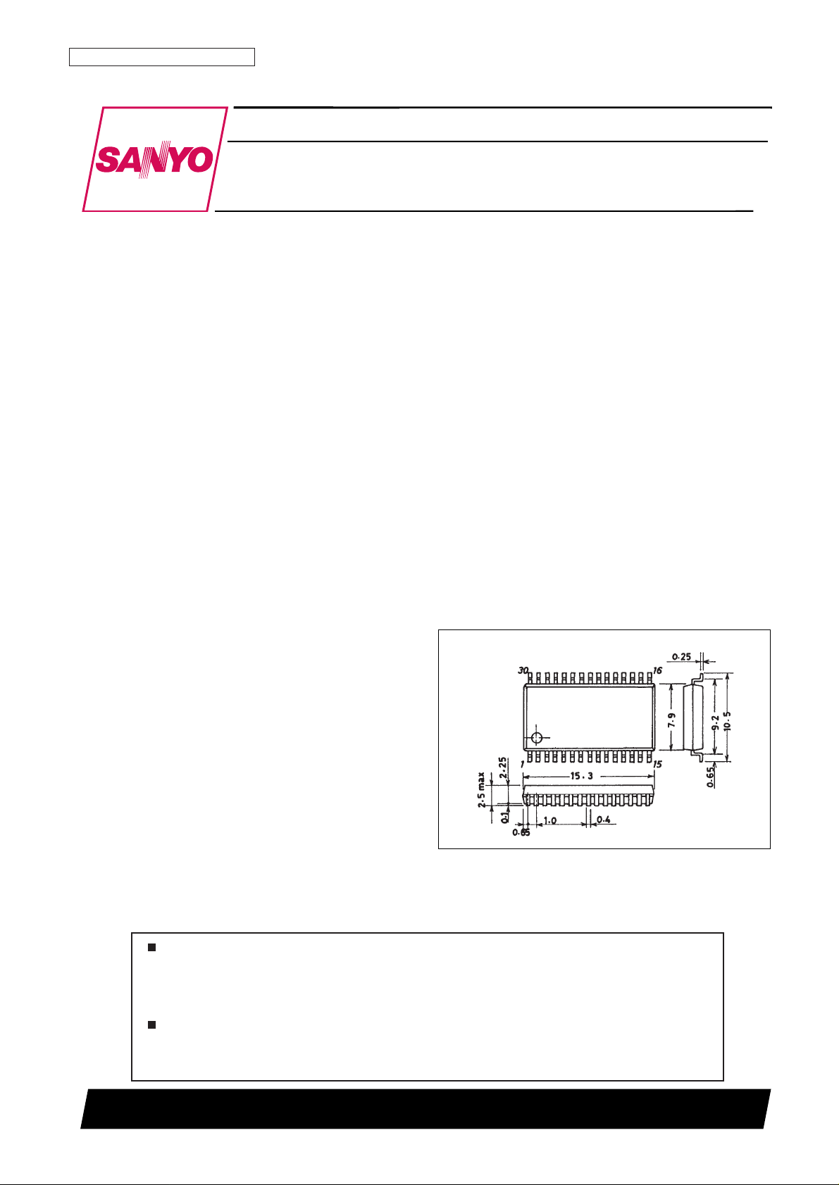
• Package: 30-pin MFP
• Power supply: 5 V, single voltage, CMOS
Package Dimensions
unit: mm
3073A-MFP30S
[LC8390M]
SANYO: MFP30S
Page 2
Pin Assignment
Block Diagram
No. 4454-2/12
LC8390M
Page 3
Pin Functions
No. 4454-3/12
LC8390M
Block Pin No. Pin I/O Function
A/D block 5 ADLV
DD
— Analog left channel A/D power supply
3 ADLV
SS
— Analog left channel A/D ground
4 ADL1 I Left channel A/D audio input
2 ADL2 O Left channel A/D linear ∆Σ output
6 ADL3 O Left channel A/D quadratic ∆Σ output
11 ADRV
DD
— Analog right channel A/D power supply
9 ADRV
SS
— Analog right channel A/D ground
10 ADR1 I Right channel A/D audio input
8 ADR2 O Right channel A/D linear ∆Σ output
12 ADR3 O Right channel A/D quadratic ∆Σ output
26 ADLRCK I A/D left and right channel clock input
25 ADBCK I A/D bit clock input
24 ADDATA O A/D data output
1 DZOUTL O A/D dithering clock output
7 DZOUTR O A/D dithering clock output
D/A block 15 DALV
DD
— Analog left channel D/A power supply
13 DALV
SS
— Analog left channel D/A ground
14 PWML O Left channel D/A PWM output
18 DARV
DD
— Analog right channel D/A power supply
16 DARV
SS
— Analog right channel D/A ground
17 PWMR O Right channel D/A PWM output
21 DALRCK I D/A left and right channel clock input
20 DABCK I D/A bit clock input
22 DADATA I D/A data input
Control and other pins 30 DV
DD
— Digital system power supply
19 DV
SS
— Digital system ground
23 CLKIN I Master clock input
28 CLKCTL I Master clock selection (high: 512 Fs, low: 384 Fs)
27 RESET I Reset input
29 TEST I Test input. (This pin must be connected to DV
DD
during normal operation.)
Page 4
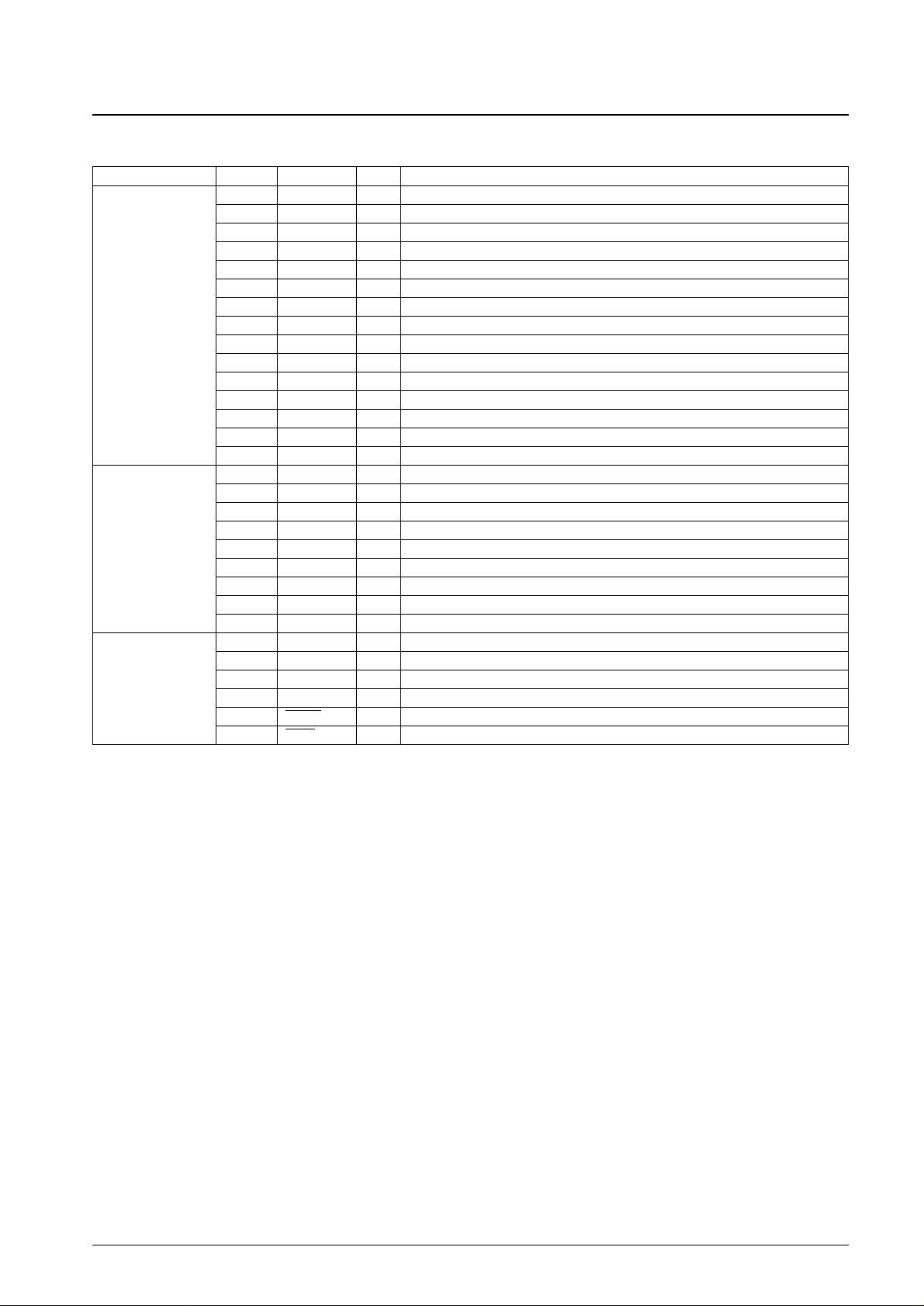
Pin Types
Specifications
Absolute Maximum Ratings at Ta = 25°C, VSS= 0 V
No. 4454-4/12
LC8390M
Parameter Symbol Conditions Ratings Unit
Maximum supply voltage V
DD
max –0.3 to +7.0 V
Maximum output voltage V
O
max –0.3 to VDD+ 0.3 V
Maximum input voltage V
IN
max –0.3 to VDD+ 0.3 V
Allowable power dissipation Pd max Ta = –30 to +70°C 200 mW
Operating temperature Topr –30 to +70 °C
Storage temperature Tstg –40 to +125 °C
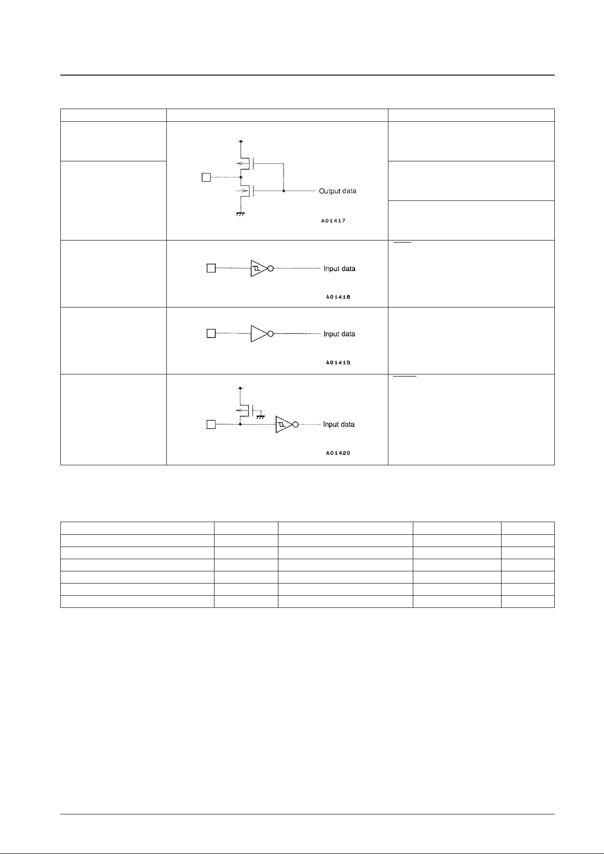
Specification Circuit Pin
TTL output ADDATA
Analog output PWML, PWMR
ADL2, ADL3, DZOUTL, ADR2, ADR3, DZOUTR
Schmitt input TEST, CLKCTL, ADLRCK, ADBCK, CLKIN,
DADATA, DALRCK, DABCK
Analog input ADL1, ADR1
Built-in pull-up resistor input RESET
Page 5

Allowable Operating Ranges
at Ta = –30 to 70°C, all V
DD
= 4.75 to 5.5 V, all VSS= 0 V unless otherwise specified
Note 1:TEST, CLKCTL, ADLRCK, ADBCK, CLKIN, DADATA, DALRCK, DABCK, RESET
2: Apply the same voltage to the DV
DD
, ADLVDD, ADRVDD, DALVDDand DARVDDpins.
Electrical Characteristics 1 at Ta = 25°C, all VDD= 5.0 V, all VSS= 0 V unless otherwise specified
Note: * A-compensation filter used, Fs = 48 kHz, and testing is performed using the Sanyo supplied evaluation board.
Electrical Characteristics 2
at Ta = –30 to 70°C, all V
DD
= 4.75 to 5.5 V, all VSS= 0 V unless otherwise specified
No. 4454-5/12
LC8390M
Parameter Symbol Conditions
Ratings
Unit
min typ max
Operating supply voltage V
DD
All VDDpins
*2
4.75 5.5 V
Input high level voltage V
IH
Schmitt inputs, built-in pull-up resistor
0.75 V
DD
V
inputs
*1
Input low level voltage V
IL
Schmitt inputs, built-in pull-up resistor
0.25 V
DD
V
inputs
*1
Frequency f
EXT
12.16 24.83 MHz
External clock
Pulse width
t
EXTH
16 ns
input conditions
t
EXTL
CLKIN: See figure 1.
Rise and fall times
t
EXTR
9 ns
t
EXTF
15 cycles of
RESET low level input pulse width t
RES
RESET: See figure 2. the CLKIN
input clock
Transfer bit t
BCYC
325 ns
clock period
Transfer bit clock t
BCW
100 ns
Transfer clock
pulse width
ADBCK, DABCK, ADLRCK, and DALRCK:
input conditions
Transfer bit clock t
BCS
See figures 3 and 4.
70 ns
setup time
Transfer bit clock t
BCH
70 ns
hold time
D/A converter data Data setup time t
DS
DABCK and DADATA: See figure 3.
70 ns
input conditions
Data hold time t
DH
70 ns
Parameter Symbol Conditions
Ratings
Unit
min typ max
Total harmonic distortion A-THD At 1 kHz and 0 dB* 0.025 %
A/D block Signal-to-noise ratio A-S/N At 1 kHz and 0 dB* 80 dB
Crosstalk A-C•T At 1 kHz and 0 dB* –78 dB
Total harmonic distortion D-THD At 1 kHz and –1 dB* 0.03 %
D/A block Signal-to-noise ratio D-S/N At 1 kHz and –1 dB* 85 dB
Crosstalk D-C•T At 1 kHz and –1 dB* –83 dB
Parameter Symbol Conditions
Ratings
Unit
min typ max
Input low-level current I
IL
RESET (built-in pull-up resistor inputs):
–250 µA
V
IN
= V
SS
Output high-level voltage V
OH
ADDATA: IOH= –0.4 mA 4.0 V
Output low-level voltage V
OL
ADDATA: IOL= 2 mA 0.4 V
Input leakage current I
LK
Schmitt inputs: VIN= VSS, V
DD
–10 +10 µA
Input and output capacitance C
IO
10 pF
Data output timing
Data hold time t
OH
ADDATA: See figure 5.
0 ns
Data delay time t
OD
50 ns
DV
DD
7 14 mA
Current dissipation I
DD
The sum of ADLVDD, ADRVDD, DALV
DD
8 16 mA
and DARV
DD
.
Page 6

Figure 1 External Clock Input Waveform (CLKIN)
Figure 2 RESET Input Waveform
Figure 3 Audio Data Input Conditions
No. 4454-6/12
LC8390M
Page 7

Figure 4 Audio Clock Input Conditions
Figure 5 Audio Data Output Timing
Master Clock Setting
Set the CLKCTL pin to match the oscillator frequency as shown in the table below.
Only the A/D converters operate when 384 Fs is selected. The D/A converters do not operate in this mode.
A/D Data Output Format
Always use the standard audio output mode when using this LSI in audio applications.
No. 4454-7/12
LC8390M
Oscillator frequency CLKCTL
512 Fs H
384 Fs L
Page 8

Standard Audio Output
Arbitrary Timing Output
The output data pin (ADDATA) holds the left channel data when ADLRCK rises, and continues to output this value
while ADLRCK remains high. Similarly, the right channel data is held when ADLRCK falls, and this value is output
while ADLRCK remains low.
D/A Data Input Format
Always use the standard audio input mode when using this LSI in audio applications.
Standard Audio Input
No. 4454-8/12
LC8390M
Page 9

Arbitrary Timing Input
The previous 16 bits of input data are valid on the rise or fall of DALRCK.
A/D Digital Filter Frequency Response (theory values, fs = 48 kHz)
Operating Principles
1. A/D Converter Block
The A/D converter block in this IC is a 2-channel 16-bit A/D converter that uses a quadratic ∆Σ modulation
technique. The circuit includes two built-in ∆Σ modulators (although an external integrator is used), and the analog
input signals are simultaneously sampled at a 128× sampling rate. The oversampled data is decimated using a digital
filter. The output data is serial signed 16-bit two’s complement data. When standard audio output is used,
simultaneously sampled data is output. When arbitrary timing is used, left channel data is output on the rise of
ADLRCK, and right channel data is output on the fall of ADLRCK.
2. D/A Converter Block
The D/A converter block in this IC is a 2-channel 16-bit D/A converter that combines a quadratic noise shaper and
PWM (pulse width modulation) techniques. Two PWM generators are built in, and quadratic noise shaping is applied
to the data, which is oversampled by holding the previous value (note that digital filters are not built in), and output
from the left and right channels at the same time. Input data is serial signed 16-bit two’s complement data. Since
digital oversampling filters are not built in, steep external low-pass filters (LPF) are required. Input data is acquired
on the rising edge of DALRCK for both standard audio input and arbitrary timing input modes. Data is output from
the PWM generators at the same time from the left and right channels.
No. 4454-9/12
LC8390M
Response (dB)
Frequency (kHz)
Page 10

3. Initialization
The LC8390M must be initialized after power is applied and when the sampling period changes. To initialize the
LC8390M, once the power supply voltage has stabilized and CLKIN has been supplied, a low level must be input to
the RESET pin for a period longer than 15 CLKIN cycles.
Design and Usage Notes
1. External Clock
The CLKIN must not be stopped during operation. If this clock is not supplied, overcurrents may occur since
dynamic logic is used internally, and the LC8390M may function abnormally. This IC must synchronize its internal
operating timing with the externally supplied ADLRCK and DALRCK. This synchronization is performed by
resetting an internal counter. This reset is only performed a few times on the rising edges of ADLRCK and
DALRCK following initialization by a RESET pin input. Therefore, the CLKIN, ADLRCK, ADBCK, DALRCK and
DABCK clock inputs must be synchronized. However, CLKIN and other clocks do not have to be synchronized for
arbitrary timing input and output. Clock jitter will degrade A/D and D/A converter precision in this IC. The wiring
lines for the master clock must be kept as short as possible, and a crystal oscillator signal level clock should be used.
2. Power Supply and Ground
Use care in supplying power and ground to this IC. Separate the analog and digital blocks, and provide a separate
ground plane for each. Connect the analog and digital grounds to points near the power supply on the PC board.
While DVDDis the power supply for the internal logic circuits, since DVDDand the analog system VDDsupplies
(ADLVDD, ADRVDD, DALVDDand DARVDD) are connected together through the IC substrate with a few Ohms
resistance, they should have identical voltages, and care should be exercised in handling the digital system power
supply.
3. A/D Block DC Offset Adjustment
A DC offset component appears in the A/D block digital output due to manufacturing variations in the IC itself and
in resistor values. When there is a DC offset, differences in the full scale level of the analog input are created. It is
therefore necessary to adjust the DC offset adjustment point in the application circuit example (see the section
“LC8390M Application Circuit Example”) while monitoring the digital output, and to cut the DC component by
performing HPF processing in the input processing block of the later stage DSP.
No. 4454-10/12
LC8390M
Page 11

No. 4454-11/12
LC8390M
Sample Application Circuit
Unit (resistance: Ω, capacitance: F)
Page 12

PS No. 4454-12/12
LC8390M
This catalog provides information as of December, 1998. Specifications and information herein are
subject to change without notice.
Specifications of any and all SANYO products described or contained herein stipulate the performance,
characteristics, and functions of the described products in the independent state, and are not guarantees
of the performance, characteristics, and functions of the described products as mounted in the customer’s
products or equipment. To verify symptoms and states that cannot be evaluated in an independent device,
the customer should always evaluate and test devices mounted in the customer’s products or equipment.
SANYO Electric Co., Ltd. strives to supply high-quality high-reliability products. However, any and all
semiconductor products fail with some probability. It is possible that these probabilistic failures could
give rise to accidents or events that could endanger human lives, that could give rise to smoke or fire,
or that could cause damage to other property. When designing equipment, adopt safety measures so
that these kinds of accidents or events cannot occur. Such measures include but are not limited to protective
circuits and error prevention circuits for safe design, redundant design, and structural design.
In the event that any or all SANYO products (including technical data, services) described or contained
herein are controlled under any of applicable local export control laws and regulations, such products must
not be exported without obtaining the export license from the authorities concerned in accordance with the
above law.
No part of this publication may be reproduced or transmitted in any form or by any means, electronic or
mechanical, including photocopying and recording, or any information storage or retrieval system,
or otherwise, without the prior written permission of SANYO Electric Co., Ltd.
Any and all information described or contained herein are subject to change without notice due to
product/technology improvement, etc. When designing equipment, refer to the “Delivery Specification”
for the SANYO product that you intend to use.
Information (including circuit diagrams and circuit parameters) herein is for example only; it is not
guaranteed for volume production. SANYO believes information herein is accurate and reliable, but
no guarantees are made or implied regarding its use or any infringements of intellectual property rights
or other rights of third parties.
 Loading...