

Page 1
Ordering number:ENN4013A
CMOS IC
LC83015E
Digital Signal Processor
for Audio Applications
Overview
The LC83015E is a digital signal processor IC designed for
medium- and high-class home audio systems, such as AV
amplifiers, mini, super-mini and car audio component systems.
The LC83015E is a part of the LC83010N/NE family. It
features an internal ROM, with a large standard program
library, an internal RAM for user programs and a wide variety of interface capabilities. The standard program library
includes sound-field simulation, theater surround and
karaoke programs.
The LC83015E operates from a 5V supply and is available
in 80-pin QFPs.
Features
• 80 ns cycle time at fs = 48kHz (256 cycles/fs)
• Dual-Harvard architecture allows single-cycle stereo signal integration and playback, with two of each of the following.
· 24 × 16-bit fixed decimal point multiplier.
· 32-bit arithmetic operation and 24-bit arithmetic logic
operation ALU/shifter.
· 32-bit accumulator.
· 8 × 32-bit temporary storage registers.
· 64 × 24-bit internal data RAM.
· 128 × 16-bit internal coefficient RAM.
· 304 × 16-bit internal coefficient ROM.
• Large program memory.
· 1024 × 32-bit standard program ROM.
· 256 × 32-bit user program RAM.
• Standard program ROM.
· Sound-field simulation library.
Auditorium simulation.
Stereo, 3-band graphic equalizer.
12-band spectrum analyzer.
· Karaoke function library.
Pitch shift (realized in program RAM)
Vocal mute.
Microphone echo.
• Coefficient ROM.
· Logarithmic conversion coefficients.
• Audio interface.
· 2 input channels compatible with a variety of formats.
· 3 output channels compatible with a variety of 32/64fs
formats.
• External memory interface.
· DRAM interface.
120 ns (maximum) RAS access time.
1Mbyte (256Kbyte × 4) or 256Kbyte (64Kbyte × 4).
1 or 2 units.
· SRAM/ROM interface.
100 ns (maximum) address access time.
1Mbyte (128Kbyte × 8) or 256Kbyte (32Kbyte × 8).
1 unit.
· Pseudo-SRAM interface.
70 ns (maximum) CE access time.
1Mbyte (128Kbyte × 8) or 256Kbyte (32Kbyte × 8).
1 unit.
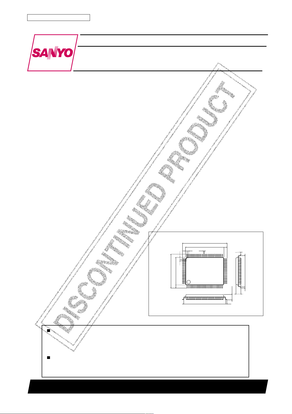
Package Dimensions
unit:mm
3174-QIP80E
[LC83015E]
17.2
23.2
0.8 0.8
1.0
64
65
0.8
14.0
80
1.6
124
0.35
20.0
21.6
1.6
0.15
41
40
25
3.0max
2.7
0.8
SANYO : QIP80E
15.6
0.8
Any and all SANYO products described or contained herein do not have specifications that can handle
applications that require extremely high levels of reliability, such as life-support systems, aircraft’s
control systems, or other applications whose failure can be reasonably expected to result in serious
physical and/or material damage. Consult with your SANYO representative nearest you before using
any SANYO products described or contained herein in such applications.
SANYO assumes no responsibility for equipment failures that result from using products at values that
exceed, even momentarily, rated values (such as maximum ratings, operating condition ranges,or other
parameters) listed in products specifications of any and all SANYO products described or contained
herein.
SANYO Electric Co.,Ltd. Semiconductor Company
TOKYO OFFICE Tokyo Bldg., 1-10, 1 Chome, Ueno, Taito-ku, TOKYO, 110-8534 JAPAN
80101TN (KT)/40893JN No.4013–1/13
Page 2
LC83015E
· Maximum external memory access per sampling period.
42/32 access for 16- /24-bit, with 2 DRAMs.
51/36 access for 16- /24-bit, with 2 SRAM.
64/42 access for 16- /24-bit, with 1 pseudo- SRAM.
• Serial microprocessor interface.
· 8-bit.
· Input and output synchronization control.
· 8 × 16-bit LIFO register.
• Other functions.
· Interrupt input.
· 4-level stack nesting.
· 12-bit interval timer.
• Compatible with LC83EV015 (PGA120) evaluation IC.
• 5V supply voltage.
• 80-pin QFP.
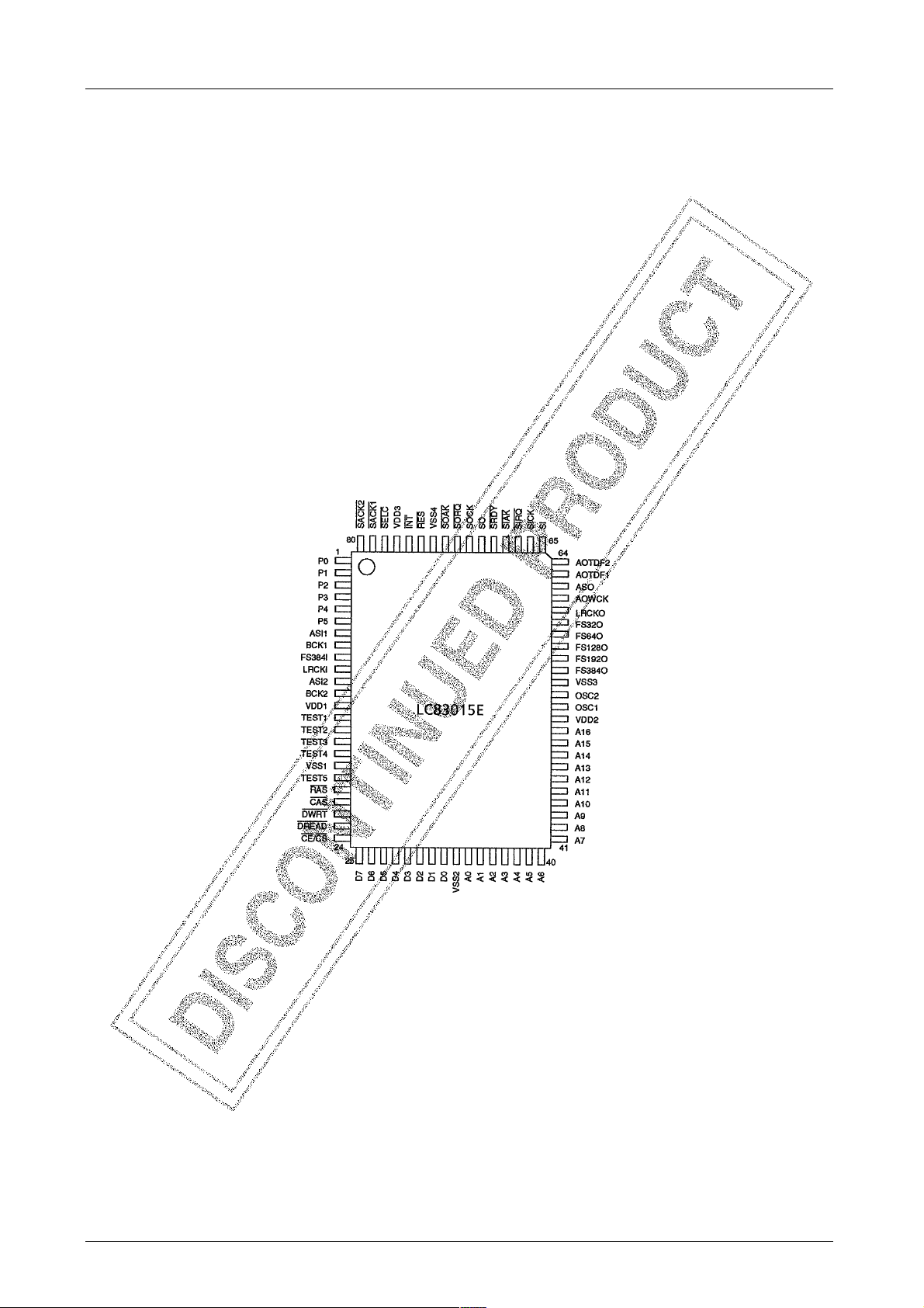
Pin Assignment
Top view
No.4013–2/13
Page 3
Pin Description
rebmuNemaN noitpircseD
6ot15Pot0P rotsiserpu-lluplanretnI.troptuptuo/tupniesoprup-lareneG
71ISA1tupnilairesatadoiduA
81KCB1ISAroftupnikcolctibsf23rosf46
9I483SFtupnisf215rosf483
01IKCRLtupnikcolclennahc-thgir/-tfeL
112ISA2tupnilairesatadoiduA
212KCB2ISAroftupnikcolctibsf23rosf46
77,15,31V
71ot414TSETot1TSET.noitarepolamronrofdnuorgottcennoC.stupnitseT
47,45,33,81V
915TSET.noitarepolamronrofnepoevaeL.tuptuotseT
02SARtuptuoSARecafretniMARD
12SACtuptuoSACecafretniMARD
22TRWDtuptuoetirwataD
32DAERDtuptuodaerataD
42SC/ECtuptuoelbanepihcMARS-oduesproMARSlanretxE
23ot520Dot7DsubatadyromemlanretxE
05ot4361Aot0AsubsserddayromemlanretxE
251CSOVottcennoC.tupnirotallicsolatsyrC
352CSO.desutonnehwnepoevaeL.tuptuorotallicsolatsyrC
55O483SF )kcolc2CSO/1CSOroI483SFsaemaS(tuptuosf215rosf483
65O291SF)O483SFfo2/1(tuptuosf652rosf291
75O821SF)O483SFfo4/1ro3/1(tuptuosf821
85O46SF)O821SFfo2/1fo1KCB(tuptuosf23rosf46
95O23SF)O46SFfo2/1(tuptuosf61rosf23
06OKCRL)O46SFfo46/1roIKCRL(tuptuosf1
16KCWOA)O46SFfo23/1(tuptuosf1rosf2
26OSA1tuptuolairesatadoiduA
361FDTOA2tuptuolairesatadoiduA
462FDTOA3tuptuolairesatadoiduA
56IStupniatadlairestib-8
66KCIStupnikcolcIS
76QRIStupnitseuqertupniatadlaireS
86KAIStuptuoegdelwonkcatupniatadlaireS
96YDRStupniydaertupniatadlaireS
07OStuptuoatadlairestib-8
17KCOStupnikcolcOS
27QROStupnitseuqertuptuoatadlaireS
37KAOStuptuoegdelwonkcatuptuoatadlaireS
57SERrotsiserpu-lluplanretnI.tupniteseR
67TNI.rotsiserpu-lluplanretnI.tupnitseuqertpurretnI
87CLES .rotsisernwod-lluplanretnI.tupninoitcelesecruoskcolcnoitcnurtsnI
971KCAS.rotsisernwod-lluplanretnI.lanimretnoitcelesO483SF
082KCAS .rotsisernwod-lluplanretnI.tupninoitcelesecruoskcolctuptuosF
LC83015E
Vot1
Vot1
3snoitcennocegatlovylppuS
DD
4snoitcennocdnuorG
SS
Vro
DD
SS
.desutonnehw
DD
SS
No.4013–3/13
Page 4
LC83015E
Specifications
Absolute Maximum Ratings
retemaraPlobmySsnoitidnoCsgnitaRtinU
V
V
egatlovylppuS
egatlovtupnIV
egatlovtuptuOV
egatlovtuptuo2CSOV
ecafretniyromemlanretxednaatadoiduA
tnerructuptuo
tnerructuptuoKAISdnaKAOS,OSI
tnerructuptuo5Pot0PI
noitapissidrewopelbawollAxamdP 007Wm
erutarepmetgnitarepOrpoT – 07+ot03
erutarepmetegarotSgtsT – 521+ot04
,1DD
Note
1. Pins ASO, AOTDF1, A OTDF2, FS384O, FS192O, FS128O, FS64O, FS32O, AOWCK, LRCKO, D0 to D7, A0 to A16,
RAS, CAS, DREAD, DWRT and CE/CS
3
,2DDVDD
I
1O
2O
I
1O
2O
3O
.1etoneeS – 4+ot2Am
– 0.7+ot3.0V
– ot3.0VDD3.0+V
– ot3.0VDD3.0+V
devorppaotpU
V
egatlovrotallicso
– 01+ot2Am
– 01+ot1Am
˚C
˚C
Recommended Operating Conditions at T a = –30 to +70˚C, V
retemaraPlobmySsnoitidnoCsgnitaRtinU
V
V
egnaregatlovylppuS
Electrical Characteristics at Ta = –30 to +70˚C, V
retemaraPlobmySsnoitidnoC
niardtnerruCI
-wolecafretniyromemlanretxednaatadoiduA
egatlovtupnilevel
-hgihecafretniyromemlanretxednaatadoiduA
egatlovtupnilevel
egatlovtupnilevel-woLV
egatlovtupnilevel-hgiHV
egatlovtupnilevel-wolecafretnilaireSV
egatlovtupnilevel-hgihecafretnilaireSV
egatlovtuptuolevel-woLV
egatlovtuptuolevel-hgiHV
tnerructupnilevel-wolTNIdnaSERI
tnerructupnilevel-wol5Pot0PI
tnerructupnilevel-wolrehtOI
tupnilevel-hgih2KCASdna1KCAS,CLES
tnerruc
tnerructupnilevel-hgiHI
latotSC/ECdnaDAERD,TRWD,SAC,SAR
tnerructuptuo
tnerructuptuolatot61Aot0Adna7Dot0D
tnerructuptuolatoT
tnerructuptuolatoT
tnerrucegakaeltuptuOI
ecnaticapactupnIC
,1DD
DD
V
V
LO
HO
1LI
2LI
3LI
I
1HI
2HI
∑IAO1
∑IAO2
∑IAO3
∑IAO4
I
V
,2DD
3DD
to V
DD1
1LI
1HI
2LI
2HI
3LI
3HI
I
Am2= 4.0
LO
I
LO
IHO=– Am4.00.4
IHO=– Aµ05
VIV=
SS
VIV=
SS
VIV=
SS
VIV=
DD
VIV=
DD
FFO
DD3
.1etoneeS 8.0V
.1etoneeS4.2V
.2etoneeS V3.0
.2etoneeSV7.0
.3etoneeS
.3etoneeS
Am01= 5.1
.6etoneeS – 5151+Am
.7etoneeS – 0101+Am
SS1
to V
SS4
= 0V
= 4.75 to 5.25 V, V
.8etoneeS.kcolclanretxezHM5205501Am
to V
SS1
V57.0
VDD– 2.1
– 052Aµ
– 0001Aµ
= 0V
SS4
sgnitaR
nimpytxam
DD
DD
– 01Aµ
– 0101+Am
– 0202+Am
– 0404+Aµ
V52.0
52.5ot57.4V
tinU
V
DD
V
V
DD
V
V
V
052Aµ
01Aµ
01Fp
Notes
1. Pins BCK1, BCK2, ASI1, ASI2, LRCKI and D0 to D7. Schmitt trigger inputs
2. Pins P0 to P5, TEST1 to TEST4, SELC, SACK1 and SACK2
3. Pins RES, INT, SI, SICK, SIRQ, SRDY, SOCK, SORQ, FS384I and OSC1. Schmitt trigger inputs
4. Pins ASO, AOTDF1, A OTDF2, FS384O, FS192O, FS128O, FS64O, FS32O, AOWCK, LRCKO, D0 to D7, A0 to A16,
RAS, CAS, DREAD, DWRT and CE/CS. TTL-level outputs
5. Pins RAS, CAS, DWRT, DREAD and CE/CS
6. Pins FS384O, FS192O, FS128O, FS64O, FS32O, LRCKO, AOWCK, ASO and AOTDF1/2
7. Pins SIAK, SRDY, SO, SOAK and P0 to P5
8. See section DESIGN NOTES for measurement conditions.
No.4013–4/13
Page 5

LC83015E
System Clock at Ta = –30 to +70˚C, V
retemaraPlobmySsnoitidnoC
ycneuqerfkcolclanretxeI483SFf
htdiweslup
doirepgnitarepOT
level-hgihdna-wolkcolclanretxeI483SF
emitllafdnaesirkcolclanretxeI483SFf
ycneuqerfrotallicsolatsyrc2CSO/1CSOf
yaledelbatsrotallicsolatsyrc2CSO/1CSOf
External Clock Timing
Oscillator Stable Delay Time
DD1
f
to V
TXE
f,
LTXE
f,
RTXE
CSO
CYC
= 4.75 to 5.25 V, V
DD3
HTXE
FTXE
SCSO
SS1
to V
SS4
= 0V
nimpytxam
sgnitaR
61.2138.42zHM
61sn
9sn
38.42zHM
001sm
97961sn
tinU
Audio Data Interface at Ta = –30 to +70˚C, V
retemaraPlobmySsnoitidnoC
doirepkcolctibtupnIt
htdiweslupkcolctibtupnIt
emitputesataDt
emitdlohataDt
yalednoitagaporpatadtuptuOt
emitdlohatadtuptuOt
CYCB
WCB
S
H
DO
HO
DD1
to V
= 4.75 to 5.25 V, V
DD3
Note
Output timing values are measured with a load capacitance of 50 pF.
Audio Data Input Timing
Audio Data Output Timing
SS1
to V
SS4
nimpytxam
= 0V
sgnitaR
523sn
001sn
07sn
07sn
05sn
0sn
tinU
No.4013–5/13
Page 6

LC83015E
Serial Data Interface at Ta = –30 to +70˚C, V
retemaraPlobmySsnoitidnoC
doirepkcolclaireSt
htdiweslupkcolclaireSt
emitputesatadtupnIt
emitdlohatadtupnIt
yalednoitagaporpatadtuptuOt
WCS
SS
HS
DS
to V
DD1
CYCS
= 4.75 to 5.25 V, V
DD3
Note
Output timing values are measured with a load capacitance of 50 pF.
Serial Data Input Timing
Serial Data Output Timing
SS1
to V
SS4
= 0V
sgnitaR
nimpytxam
084sn
002sn
07sn
07sn
tinU
001sn
External DRAM Interface at T a = –30 to +70˚C, V
retemaraPlobmySsnoitidnoC
emitputesatadtupnIt
emitdlohatadtupnIt
htdiwesluplevel-wolSACt
htdiwesluplevel-hgihSACt
htdiwesluplevel-wolSARt
htdiwesluplevel-hgihSARt
doirepSACt
yalednoitagaporpSACotSARt
emitdlohSACt
emitdlohSARt
emitputessserddaSARt
emitdlohsserddaSARt
emitputessserddaSACt
emitdlohsserddaSACt
htdiweslupTRWDt
emitputesdnammocetirWt
emitdlohdnammocetirWt
emitputesatadtuptuOt
emitdlohatadtuptuOt
1ISD
1IHD
SAC
PC
SAR
PR
CP
DCR
HSC
HSR
RSA
HAR
CSA
HAC
PW
SCW
HCW
1OSD
1OHD
DD1
to V
DD3
Note
Output timing values are measured with a load capacitance of 50 pF.
= 4.75 to 5.25 V, V
to V
SS1
nimpytxam
51sn
0sn
57sn
57sn
053sn
011sn
061sn
011sn
091sn
07sn
041sn
03sn
07sn
07sn
57sn
03sn
03sn
05sn
05sn
SS4
= 0V
sgnitaR
tinU
No.4013–6/13
Page 7

External DRAM Input Timing
External DRAM Output Timing
LC83015E
External SRAM Interface at Ta = –30 to +70˚C, V
retemaraPlobmySsnoitidnoC
emitputesatadtupnIt
emitdlohatadtupnIt
emitelcycetirw/daeRt
emitputessserddAt
emityrevoceretirWt
htdiweslupTRWDt
emitputesatadtuptuOt
emitdlohatadtuptuOt
2ISD
2IHD
CWR
SA
RW
PW
2OSD
2OHD
DD1
to V
DD3
Note
Output timing values are measured with a load capacitance of 50 pF.
= 4.75 to 5.25 V, V
SS1
to V
= 0V
SS4
nimpytxam
06sn
0sn
061sn
01sn
03sn
57sn
05sn
03sn
sgnitaR
tinU
No.4013–7/13
Page 8

External SRAM Input Timing
External SRAM Output Timing
LC83015E
External Pseudo-SRAM Interface at Ta = –30 to +70˚C, V
retemaraPlobmySsnoitidnoC
emitputesatadtupnIt
emitdlohatadtupnIt
doirepSC/ECt
htdiweslupSC/ECt
emitegrahc-erpSC/ECt
emitputessserddaSC/ECt
emitdlohsserddaSC/ECt
emitdlohdnammocetirWt
emitdaerdnammocetirWt
htdiweslupTRWDt
emitputesatadtuptuoTRWDt
emitdlohatadtuptuoTRWDt
emitputesatadtuptuoSC/ECt
emitdlohatadtuptuoSC/ECt
yalednoitagaporpDAERDotSC/ECt
3ISD
3IHD
C
SEC
P
CSA
CHA
HCW
LWC
PW
WSD
WHD
CSD
CHD
RED
DD1
Note
Output timing values are measured with a load capacitance of 50 pF.
to V
= 4.75 to 5.25 V, V
DD3
to V
SS1
nimpytxam
01sn
0sn
061sn
57sn
57sn
51sn
001sn
07sn
07sn
57sn
05sn
03sn
05sn
03sn
003sn
= 0V
SS4
sgnitaR
tinU
No.4013–8/13
Page 9

External Pseudo-SRAM Input Timing
External Pseudo-SRAM Output Timing
LC83015E
Design Notes
When SELC is LOW, the LC83015E system clock is generated from FS384I. When SELC is HIGH, it is generated
from the free-running oscillator, OSC1. When SACK1 is
LOW, FS384O output is 1/3 of FS128O output. When
SACK1 is HIGH, it is 1/4 of FS128O output. W hen SA CK2
is LOW, the output clock is generated from FS384I, LRCKI
and BCK1. When SACK2 is HIGH, it is generated from the
free-running oscillator, OSC1.
When the LC83015E is used with one DRAM unit, only
D0 to D3 of the data bus are used. When the LC83015E is
used with two DRAM units, SRAM or pseudo-SRAM, D0
to D7 are used.
The typical supply current, I
, is measured with SANYO
DD
Standard Theatre Mode in operation under the input/output
conditions shown in figure 1.
No.4013–9/13
Page 10

LC83015E
Figure 1. Measurment conditions for I
DD
No.4013–10/13
Page 11

LC83015E
The LC83015E has three voltage supply pins (VDD1 to
VDD3) and four ground pins (VSS1 to VSS4). The connections between these pins must conduct sufficiently to ensure that there are no voltage differences between each of
the voltage supply pins and each of the ground pins when
the device is powered-up. Connections similar to those
shown in figure 2 should be used.
Figure 3 shows the connection of a crystal oscilator to the
LC83015E Table 1 shows oscillator frequencies and capacitances for a Nippon Denpa Kogyo NR-18 crystal oscillator .
Figure 3. Crystal oscillator connection
Table 1. Oscillator frequency selection
)Fp(2C,1C)zHM(ycneuqerfrotallicsO
81882.21
214439.61
01234.81
21438.61
82975.22
6675.42
Figure 2. Voltage supply and ground connection template
No.4013–11/13
Page 12

LC83015E
LC83015E Development Environment
The following software tools are available.
• LC83015.EXE assembler
• S83015.EXE debugger and simulator
• STI.EXE ROM sorting software for microprocessor
• STO.EXE ROM sorting software for external ROM
The following hardware tools are intended for use with the
LC83015E.
• IBM PC/AT or AX personal computer
• In-Circuit Emulator (ICE) comprising
ICE83015
POD83
IC149-080-021-S5
E83015.EXE software
• Simple model evaluation board comprising
PRBD15
D2SP.EXE software
Figure 4. ICE configuration
Figure 5. Model board configuration
No.4013–12/13
Page 13

Application Example
LC83015E
Note
The LC83015E is in external synchronization mode in this application.
Specifications of any and all SANYO products described or contained herein stipulate the performance,
characteristics, and functions of the described products in the independent state, and are not guarantees
of the performance, characteristics, and functions of the described products as mounted in the customer's
products or equipment. To verify symptoms and states that cannot be evaluated in an independent device,
the customer should always evaluate and test devices mounted in the customer's products or equipment.
SANYO Electric Co., Ltd. strives to supply high-quality high-reliability products. However, any and all
semiconductor products fail with some probability. It is possible that these probabilistic failures could
give rise to accidents or events that could endanger human lives, that could give rise to smoke or fire,
or that could cause damage to other property. When designing equipment, adopt safety measures so
that these kinds of accidents or events cannot occur. Such measures include but are not limited to protective
circuits and error prevention circuits for safe design, redundant design, and structural design.
In the event that any or all SANYO products(including technical data,services) described or
contained herein are controlled under any of applicable local export control laws and regulations,
such products must not be exported without obtaining the export license from the authorities
concerned in accordance with the above law.
No part of this publication may be reproduced or transmitted in any form or by any means, electronic or
mechanical, including photocopying and recording, or any information storage or retrieval system,
or otherwise, without the prior written permission of SANYO Electric Co. , Ltd.
Any and all information described or contained herein are subject to change without notice due to
product/technology improvement, etc. When designing equipment, refer to the "Delivery Specification"
for the SANYO product that you intend to use.
Information (including circuit diagrams and circuit parameters) herein is for example only ; it is not
guaranteed for volume production. SANYO believes information herein is accurate and reliable, but
no guarantees are made or implied regarding its use or any infringements of intellectual property rights
or other rights of third parties.
This catalog provides information as of August, 2001. Specifications and information herein are subject to
change without notice.
PS No.4013–13/13
 Loading...