

Page 1

Ordering number:ENN3945A
CMOS IC
LC83010N, 83010NE
Audio Digital Signal Processor
Overview
The LC83010N, 83010NE is a single-chip digital signal
processor (DSP). It is designed for use in the application
fields such as a digital processing of audio signals.
The LC83010N, 83010NE CMOS processor has various
on-chip filtering circuits such as a graphic equalizer for
reproduction of sound quality. It also has simulation circuit for reverberation (sound reflection and echo), so that
sound field with surround and delay can be created.
The LC83010N and LC83010NE are upgraded versions of
the LC83010 and the LC83010E. The LC83010N and
LC83010NE have a 64fs clock output that enables improved
interfacing with external A/D converters. TEST5 has been
renamed FS640/T5 and incorporates both the new clock
output and the original test output.
Features
LSI functions
• Dual Harvard Architecture: Enables simultaneous processing (multiply and addition) of stereo signals in a single
instruction cycle.
The LC83010N, LC83010NE processor has the following two independent units:
· Multiplier : 24 bits × 16 bits (fixed-point decimal)
· ALU : 32-bit arithmetic calculation, 24-bit arithmetic
and logical operations.
· ACCumulator (ACC) : 32 bits
· Temporal Registers (TMP0 to TMP7) : 32-bit for each
· Internal Memory Data RAM 128 × 24 bits
Coefficient RAM 256 × 16 bits
Constant ROM 256 × 24 bits
• Program memory Capacity (RAM) : 320 × 32 bits
• A variety of I/O interfaces.
· Audio signal I/O :
1 channel for input (applicable to various formats)
3 channel for output (applicable to up to 4 types of data
format)
· Surround DRAM access signal :
16 accesses/CH Max. (within 1 fs)
Up to 2 256K (64K × 4 bits) DRAMs or 1M (256K × 4
bits) DRAMs can be directly connected to this chip.
· Uses external DRAMS with RAS access times of 120
ns or lower.
· Serial input/output interface with a microcomputer.
Synchronous 8-bit serial input : 1
[Mail box (16 bits × 8) function available]
Synchronous 8-bit serial output : 1
• Interrupt function (Vectored interrupt with the INT pin)
• Stack Nesting Levels : 4
• On-chip Interval Timer :
12 bits (timer clock = sampling frequency)
• Cycle time : 108ns (sampling frequency = 48kHz)
• Single 5V power supply.
• Package : 64-pin DIPs (LC83010N).
80-pin QFPs (LC83010NE).
Note) When soldering QFP devices, do not use the solder
dip method.
• Evaluation chip : LC83EV010N (PGA100)
· Applications
· Graphic Equalizer
· Power calculation for spectrum analyzer display
· Sound field creation (using external DRAMs)
· 4 Speakers + REC output
Development Environment
• Software Tools
· Assembler
· Debugger with simulation
• Hardware Tools
· IBM PC-AT compatible machines or AX per sonal computers
· In Circuit Emulator (ICE)
Any and all SANYO products described or contained herein do not have specifications that can handle
applications that require extremely high levels of reliability, such as life-support systems, aircraft’s
control systems, or other applications whose failure can be reasonably expected to result in serious
physical and/or material damage. Consult with your SANYO representative nearest you before using
any SANYO products described or contained herein in such applications.
SANYO assumes no responsibility for equipment failures that result from using products at values that
exceed, even momentarily, rated values (such as maximum ratings, operating condition ranges,or other
parameters) listed in products specifications of any and all SANYO products described or contained
herein.
SANYO Electric Co.,Ltd. Semiconductor Company
TOKYO OFFICE Tokyo Bldg., 1-10, 1 Chome, Ueno, Taito-ku, TOKYO, 110-8534 JAPAN
O1001TN (KT)/N251JN KI No.3945–1/18
Page 2
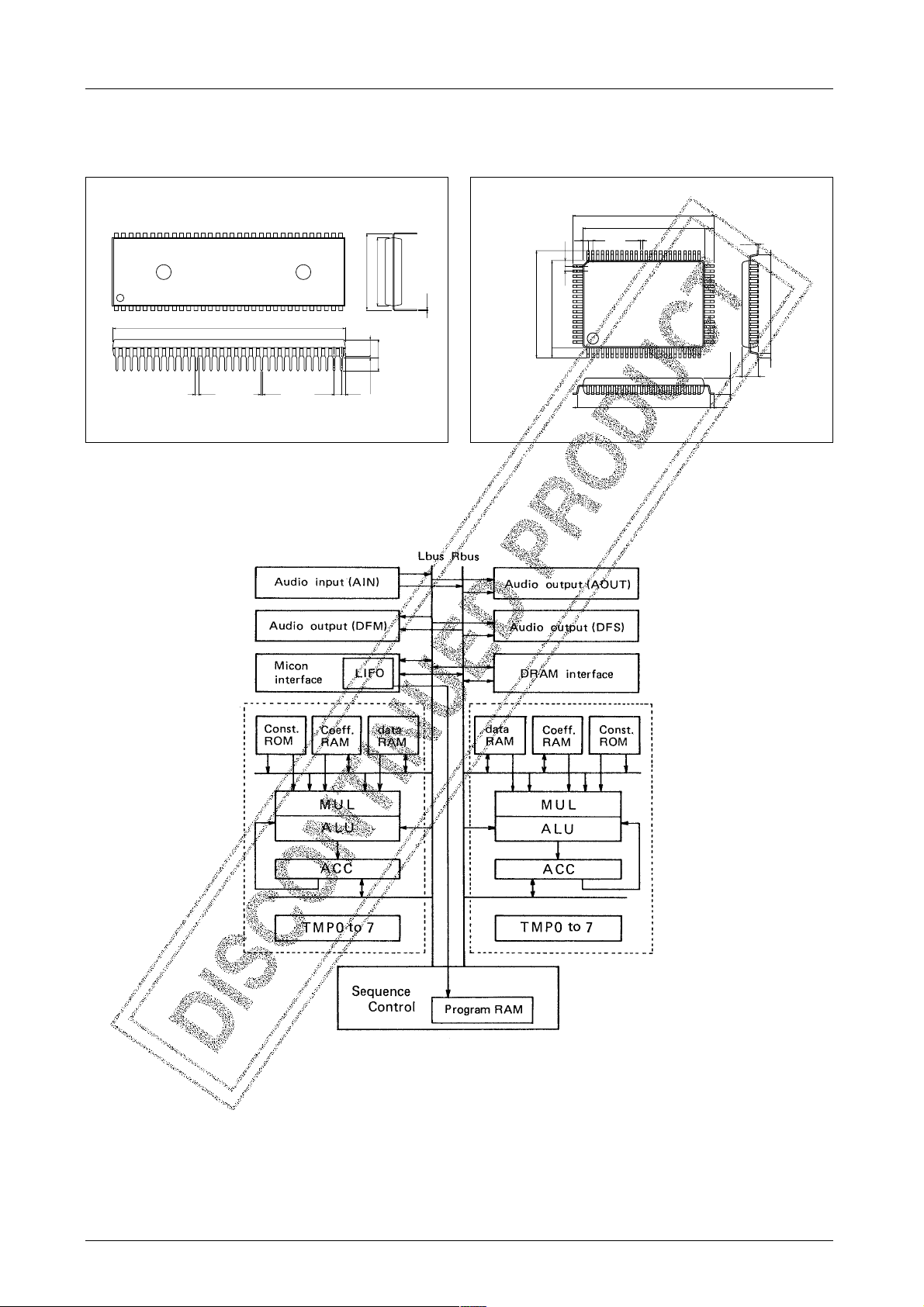
Package Dimensions
unit:mm
3071-DIP64S
[LC83010N]
57.2
0.95 0.48 1.78 1.01
Block Diagram
LC83010N, 83010NE
unit:mm
3174-QIP80E
3364
16.8
19.05
5.0max
3.2
0.25
321
4.0
0.51min
SANYO : DIP64S
17.2
[LC83010NE]
23.2
0.8 0.8
1.0
64
65
0.8
14.0
80
1.6
124
0.35
20.0
21.6
1.6
0.15
41
40
25
3.0max
2.7
0.8
SANYO : QIP80E
15.6
0.8
No.3945–2/18
Page 3
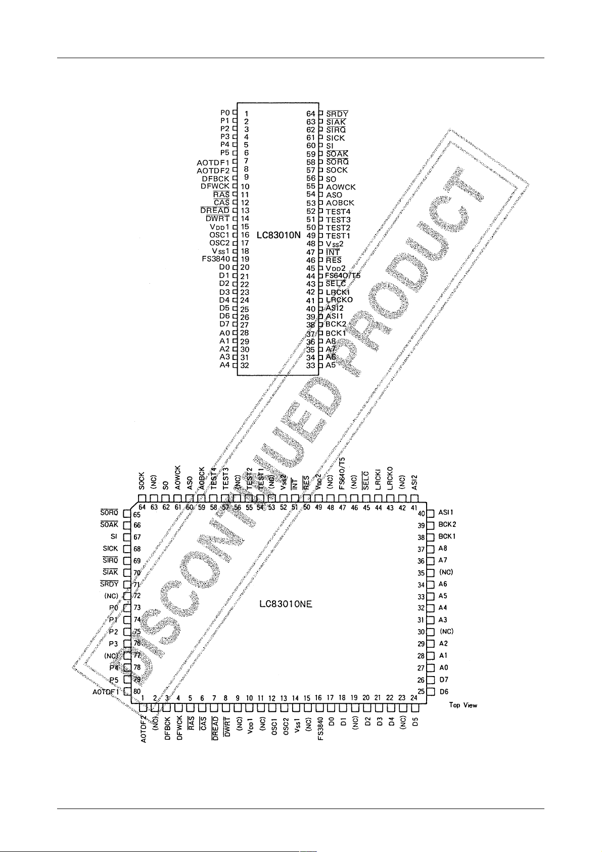
Pin Assignments
(DIP64S)
LC83010N, 83010NE
(QIP80E)
Top view
No.3945–3/18
Page 4
Pin Function
emaNniPO/I noitpircseDlanoitcnuF
VDD2,1
VSS2,1
1ISA
2ISA
1KCB
2KCB
IKCRL
OKCRL
OSA
KCBOA
KCWOA
Audio I/F (Interface)
DRAM I/F
Microcomputer I/F
Control pins
1FDTOA
2FDTOA
KCBFD
KCWFD
SAR
SAC
DAERD
TRWD
8ot0A
7ot0D
IS
KCIS
QRIS
KAIS
YDRS
OS
KCOS
QROS
KAOS
5ot0PO/I)rotsiserpu-lluppihc-nohtiw(stroptuptuO/tupnIesoprup-lareneG
1CSO
2CSO
O483SFOniptuptuosf483
TNII )rotsiserpu-lluppihc-nohtiw(niptupnitseuqertpurretnI
SERI )rotsiserpu-lluppihc-nohtiw(niptupniteseR
CLESI
5T/O46SF
LC83010N, 83010NE
I
I
I
I
I
O/I
I
O
O
O
O
O
O
O
O
O
O
O
O
O
O/I
I
I
I
O
I
O
I
I
O
I
O
4ot1TSET
I
O
)tuptuo
1tupnilairesatadoiduA
2tupnilairesatadoiduA
atad1ISArofniptupnikcolctiB
)RCybelbatcelesO/I(atad2ISArofniptupnikcolctiB
tuptuolairesatadoiduA
)sf84dnasf23rof(atadOSArofniptuptuokcolctiB
atadOSArofniptuptuokcolcdroW
)1ecneserphgihrof(atadoiduarofniptuptuolaireS
)2ecneserphgihrof(atadoiduarofniptuptuolaireS
)sf84dnasf23rof(atad2FDTOAdna1FDTOArofniptuptuokcolctiB
atad2FDTOAdna1FDTOArofniptuptuokcolcdroW
sMARDlanretxeotlangisSARrofniptuptuO
sMARDlanretxeotlangisSACrofniptuptuO
sMARDlanretxeotlangisdaeratadrofniptuptuO
sMARDlanretxeotlangisetirwatadrofniptuptuO
K46(sMARDlanretxeotslangissserddarofsniptuptuO × K652,7Aot0A:stib4 × )8Aot0A:stib4
.desuera7Dot0Dsnip,edomnoitarugifnocMARDelbuodehtnI.desu
)atadlairestib-8(retupmocorcimlortnocmorfatadlairesrofniptupnI
atadISrofniptupnikcolclaireS
tupniatadlairesrofniptupnilangistseuqeR
)atadlairestib-8(retupmocorcimgnillortnocaotatadlairesrofniptuptuO
atadOSrofniptupnikcolclaireS
tuptuoatadlairesrofniptupnilangistseuqeR
.noitarepolamrongnirudsretrevnocD/Alanretxeroftuptuokcolc
).ecruosrewopevitisopehtotdetcennocebdluohssnipesehT(snipylppusrewopV5+
).leveldnuorgehtotdetcennocebdluohssnipesehT(snipylppusrewopDNG
)atadlennahcR:L;atadlennahcL:H(langishsiugnitsidlennahcR/LrofniptupnI
)atadlennahcR:L;atadlennahcL:H(langishsiugnitsidlennahcR/LrofniptupnI
era3Dot0Dsnip,edomnoitarugifnocMARDelgnisehtnI.sMARDlanretxehtiwrefsnartatadrofsniptuptuo/tupnI
retupmocorcimamorflangistseuqertupniehtotesnopseregdelwonkcArofniptuptuO
refsnartatadafodneehtgnitacidniretupmocorcimgnillortnocamorflangisydaeRarofniptupnI
retupmocorcimamorflangistseuqertuptuoehtotesnopseregdelwonkcArofniptuptuO
)sf483(.ecruoslanretxenamorftupnikcolcrofrorotallicsolatsyrcahtiwnoitcennocrofniP
)edomtupnikcolclanretxeninepotfelebdluohs(rotallicsolatsyrcahtiwnoitcennocrofniP
redividlanretni(lanretni:H,)IKCRL(lanretxe:L;rotsisernwod-lluppihc-nohtiwniptupnitceleslangislennahcR/L
.leveldnuorgehtotdetcennocebdluohssnipeseht,yllamroN.sniptupnilangistseT
sf46asadnaedomtsetnituptuotsetasasnoticnuf5T/O46SF.tuptuotset/tuptuokcolcsf46.sniptuptuolangistseT
No.3945–4/18
Page 5
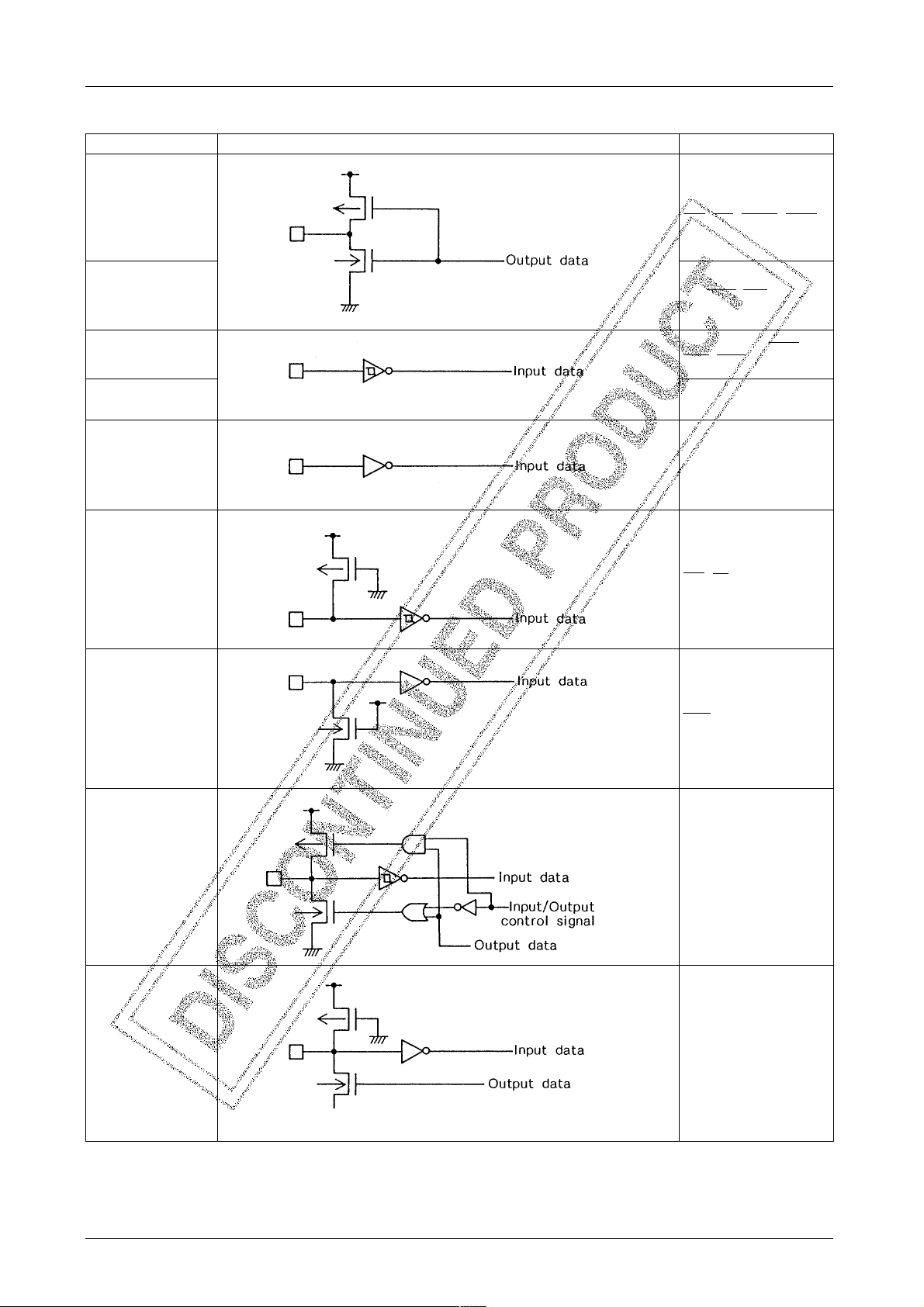
Pin Configuration Types
noitacificepsleveL epyttiucriCemaNniP
tuptuolevelLTT
LC83010N, 83010NE
,KCWOAKCBOA,OSA
,2FDTOA,1FDTOA,OKCRL
,O483SF,8Aot0A,KCWFD
5T/O46SF
,TRWD,DAERD,SAC,SAR
levelmuidemSOMC
tuptuotnerruc
tupnittimhcS
tupnittimhcSlevelL IKCRL,2ISA,1ISA,1KCB
tupnilamroN 4ot1TSET
rotsiser
rotsisernwod
pu-lluplanretnihtiwtupnI
-lluplanretnihtiwtupnI
KAIS,KAOS,OS
YDRS,QRIS
TNI,SER
CLES
,QROS,KCIS,IS,KCOS
tuptuolevelLTT
tupnittimhcSlevelwoL
tuptuo
tupnilamroN
tnerrucmuidemSOMuP
7Dot0D,2KCB
5Pot0P
No.3945–5/18
Page 6
LC83010N, 83010NE
Specifications
Absolute Maximum Ratings at Ta = 25˚C, VSS = 0V
retemaraPlobmySsnoitidnoCsgnitaRtinUetoN
egatlovylppusmumixaMV
egatlovtuptuO
egatlovtupnIVNI– ot3.0VDD3.0+V
tnerructuptuokaeP
tnerructuptuoegarevA
noitapissidrewopelbawollAxamdP 006Wm
erutarepmetgnitarepOrpoT – 07+ot03
erutarepmetegarotSgtsT – 521+ot04
xam – 0.7+ot3.0V
DD
10Vtuptuo2CSO
20V2CSOehtroftpecxesniP – ot3.0VDD3.0+V
IPO1F/IMARD,F/IoiduA – 4+ot2Am1
IPO2F/IretupmocorciM – 01+ot2Am2
IPO35Pot0P – 01+ot5.0Am3
IAO1nipreP:F/IoiduA – 4+ot2Am4
IAO2nipreP:F/IMARD,F/IoiduA – 4+ot2Am5
IAO3nipreP:F/IretupmocorciM – 01+ot2Am2
IAO4nipreP:5Pot0P – 01+ot5.0Am3
∑IAO1
∑IAO2
∑IAO3
∑IAO4
Ta=–30 to +70˚C
egatlovehtotpU
ybdecudorp
noitallicso
latoT:F/IoiduA – 54+ot11Am4
latoT:F/IMARD,F/IoiduA – 51+ot4Am5
latoT:F/IretupmocorciM51+ot4Am2
latoT:5Pot0P – 03+ot3Am3
V
˚C
˚C
* When soldering QFP devices, do not use the solder dip method.
Allowable Operating Conditions at T a = –30 to +70˚C, V
retemaraPlobmySsnoitidnoC
External clock
input conditions
Self-oscillation
conditions
Crystal oscillation
egatlovylppusgnitarepOV
egatlovlevel-hgihtupnI
egatlovlevel-woltupnI
)emitelcycnoitcurtsnI(ycneuqerfgnitarepO
ycneuqerFf
htdiwesluP
emitesiR
emitllaF
ycneuqerfnoitallicsof
doirepgnizilbatsnoitallicsof
DD
VHI1F/IMARD,F/IoiduA4.2V6
VHI24ot1TSET,CLES,5Pot0PV7.0
VHI3F/IretupmocorciM,TNI,SER
VLI1F/IMARD,F/IoiduA 8.0V6
VLI24ot1TSET,CLES,5Pot0PV3.0
VLI3F/IretupmocorciM,TNI,SER
f
PO
)CYCT(
TXE
f
HTXE
f
LTXE
f
RTXE
f
FTXE
TXE
STXE
DD
zHk84:xam × 483 × 10.1
.1erugifeeS
.3erugifeeS sm
= 4.75V to 5.25V, VSS = 0V, unless otherwise noted
sgnitaR
nimpytxam
57.452.5V
DD
V57.0
DD
V52.0
.dewollasirorrenoitallicsoaltsyrc%1otpU
.nip1CSOehtotseilppA
)nepo:2CSO,tupni:1CSO(
.2erugifeeS,2CSO,1CSO 26.81zHM
71.21
)561(
71.2126.81zHM
02sn
V
V7
V
DD
V7
DD
26.81
sn)701(
01sn
tinUetoN
zHM
)sn(
emitputesataDt
Audio data input conditions
emitdlohataDt
elcyckcolctibrefsnarTt
htdiweslupkcolctibrefsnarTt
CYCB
WCB
.4erugifeeS
S
H
523sn
001sn
.snip2KCBdna1KCBehtotseilppA
57sn
57sn
Continued on next page.
No.3945–6/18
Page 7

Continued from preceding page.
retemaraPlobmySsnoitidnoC
elcyckcolclaireSt
LC83010N, 83010NE
CYCS
sgnitaR
nimpytxam
056sn
tinUetoN
Serial I/O clock conditions
DRAM input
conditions
htdiweslupkcolclaireSt
emitputesataDt
emitdlohataDt
emitputesataDt
emitdlohataDt
WCS
.5erugifeeS
SS
HS
SD
.6erugifeeS.MARD
HD
.ecafretniretupmocorcimehtotseilppA
).snipISdnaKCOS,KCISehtotseilppA(
lanretxemorftupniatadehtotseilppA
)7Dot0DdnaSAC,SARneewtebsgnimiT(
523sn
57sn
57sn
14sn8
0sn8
Electrical Characteristics at T a = –30 to +70˚C, VDD = 4.75V to 5.25 V, VSS = 0V, unless otherwise noted
sgnitaR
02sn
001sn
Audio data
output timing
retemaraPlobmySsnoitidnoC
tnerruclevel-woltupnI
tnerruclevel-hgihtupnIIHIrotsisernwod-lluphtiwniptupnI,CLES 052Aµ
egatlovlevel-hgihutptuO
egatlovlevel-woltuptuO
tnerrucegakaeltupnIV
tnerrucegakaelffo-tuptuOI
ecnaticapactuptuo/tupnI 01Fp
emitdlohatadtuptuOt
yaledatadtuptuOt
ILI1V,TNI,SER
ILI2V,5Pot0P
VHO1IHO=– Am4.00.4V1
VHO2IHO=– Aµ05
VLO1IHOAm2=4.0V 1
VLO2IHOAm01=5.1V 3,2
NI
VOV=
FFO
HO
DO
NIV=SS
NIV=SS
V=
V
otSS
DD
,SSVDD
.7erugifeeS
.tuptuoatadoiduaotseilppA
nimpytxam
– 052Aµ
–1Am
VDD– 2.1
– 0101+Aµ
– 0404+Aµ
tinUetoN
V3,2
.tuptuoatadlairesotseilppA
59sn8
051sn8
08sn8
101sn8
.MARDlanretxerofgnimittuptuoataD
wolebemitsseccaSARsahhcihwMARD
.desuebdluohssn021
kcolclanretxezHM26.81,2,105001Am
0sn8
02sn8
0sn8
04sn8
05sn8
0sn8
0sn8
05sn8
001sn
Microcomputer
I/F output delay
Access timings for external DRAM
niardtnerruCI
yaledatadtuptuOt
htdiweslupHSARt
htdiweslupLSARt
htdiweslupHSACt
htdiweslupLSACt
emitputessserddaSARt
emitdlohsserddaSARt
emitputessserddaSACt
emitdlohsserddaSACt
htdiweslupTRWDt
emitputesETIRW-erofeb-SACt
emitputesataDt
emitdlohataDt
noitallicsolatsyrC2C,1C.2erugifeeS,2CSO,1CSO02Fp
DS
PR
SAR
PC
SAC
SR
HR
SC
HC
W
CW
DS
DH
V
DD
.8erugifeeS
.9erugifeeS
)etoN(
DD
(Note 1) TTL level output pins: ASO, AOBCK, AOWCK, LRCK O, BCK2, AOTDF1, AOTDF2, DFBCK, DFWCK, D0 to
D7, A0 to A8, FS384O, RAS, CAS, DREAD, DWRT and FS64O/T5
(Note 2) CMOS medium current outputs: SO, SOAK, and SIAK
(Note 3) Pu MOS medium current outputs: P0 to P5
(Note 4) TTL level outputs (first group): ASO, AOBCK, AOWCK, LRCKO, A0 to A8, D0 to D7, FS384O and BCK2
(Note 5) TTL level outputs (second group): AOTDF1, AOTDF2, DFWCK, RAS, CAS, DREAD, DWRT, and DFBCK
(Note 6) L level Schmitt inputs pin: BCK1, BCK2, ASI1, ASI2, LRCKI, and D0 to D7
(Note 7) Schmitt input pins: RES, INT, SOCK, SI, SICK, SORQ, SIRQ, and SRDY
(Note 8) The maximum load capacitance of RAS, CAS, DREAD, DWRT, D0 to D7 and A0 to A8 is 50pF.
No.3945–7/18
Page 8

LC83010N, 83010NE
No.3945–8/18
Page 9

LC83010N, 83010NE
No.3945–9/18
Page 10

LC83010N, 83010NE
Program Load to The LC83010N
- Boot procedure -
2
Programs must be loaded (boot strap) into the LC83010N (D
its internal program memory consists of RAMs. The capacity of the program memory is 320 words × 32 bits.
The procedural flow to load a 320-word program into the D2SP from a controlling microcomputer is shown in Figure A-
1.
2
(1) Reset the entire system (microcomputer and D
SP) or reset the D2SP from the controlling microcomputer.
After the D2SP is reset, it then enters the Boot mode.
2
(2) Transfer the program to the D
SP from the microcomputer. The program is transferred to the D2SP in 8-bit synchro-
nous serial communication mode.
The program data of 8 bits × 16 data (equal to 4 instructions) is transferred to the D2SP continuously from the
microcomputer, and follo wed by the SRDY signal. The D2SP stores that program data of 4 instructions to the internal
mail box. The program data is then moved to the program RAM at the moment when the SRDY signal reaches the
2
SP.
D
(3) The operations discussed in (2) are repeated 80 times until the program data transfer of 320 instructions from the
2
microcomputer to the D
SP is complete.
(4) The D2SP automatically starts the program execution when the program loading of 320 instructions is complete.
The program is transferred to the D2SP from the microcomputer in that manner.
SP) from an external control unit (microcomputer) because
Figure A-1. Example Program Boot Flow (D2SP ← Microcomputer)
No.3945–10/18
Page 11

LC83010N, 83010NE
Figure A-2 gives the outline of an example program Boot system.
Figure A-2. Outline of an Example Program Boot System
Development Tool System
- Program development flow Development tools are provided to help the user to easily
2
develop application programs for the D
SP. These
development tools are divided into two groups: software
support tool group and hardware support tool group. The
software support tool group consists of an assembler,
debugger and simulator.
The hardware support tool group is realized as an InCircuit Emulator (ICE).
Figure A-3 shows the applications development flow for
2
SP system.
the D
(1) Write an application source program.
(2) Check the source program for syntax errors with the
assembler. If every syntax error is corrected, the
assembler generates a HEX program file.
(3) Check the HEX file for operational errors with the
simulator. If the desired operations are not successful,
start the debugger to find what caused logical errors.
(4) If program operations are checked successfully, use
the ICE to evaluate the audio signal output.
First, evaluate sound signals only with the ICE. In this
evaluation process, the delay memory and microcomputer of the ICE are used.
Second, start the total evaluation on an application
system. In this evaluation stage, the AD/DA converters, microcomputer, and delay memory on the user
application system are used.
Figure A-4 shows the entire program development
2
tool system for the D
SP.
The software tools such as the assembler, debugger,
simulator can be run on an IBM PC-AT compa tible
machine or an AX personal computer. The ICE is also
controlled by such a host personal computer.
Figure A-3. Applications Development Flow
No.3945–11/18
Page 12

LC83010N, 83010NE
Figure A-4. Entire Support Tool System for Microprogram Development
(1) Debugger
2
The debugger is a software support tool designed to realize virtual D
SP functional circuits. In this virtually
emulated D2SP environment, user application programs can be evaluated as if they were executed on the real chip.
The debugger is used mainly for logics analysis and detailed data analysis.
Major functions of the debugger are listed in the table below, with brief explanation for each.
· Display and Edit instructions
These instructions can be used to display the contents of memory and registers on a screen and to update them.
· Memory Fill instruction
This instruction is used to fill a specified memory address range with a desired value.
· Move instruction
This instruction is used to transfer the data in a specified memory address range to another range.
· Memory Load and Save instructions
These instructions are used to transfer data between memory and disk. The memory load instruction enables the
data transfer from a disk file to memory while the memory save instruction allows the data transfer from memory
to a disk file.
· Assemble and Unassemble instructions
The assemble instruction is used to convert mnemonics into machine codes.
The unassemble instruction is used to convert memory data back to mnemonics.
· Emulation instruction control instruction and Break point instruction
2
These instructions are used to execute the D
SP program and trace its operations. The break point instruction is
used to set a point where the program execution stops.
Table Major debugger functions
No.3945–12/18
Page 13

LC83010N, 83010NE
(2) Outline of the simulator functions
The application programs can be tested in the following sequence:
2
· Inputting digital audio signals to the D
· Executing a program,
· Converting the audio output into analog signals, and
· Measuring the analog signals with an oscilloscope or frequency characteristics meter (or sweep meter).
The simulator enables the above operations on a personal computer.
Figure A-5 shows the signal waveform measurement.
This simulator has the following three measurement functions:
1) Audio output waveforms (sine waves) with respect to audio input waveforms (sine waves)
2) Frequency characteristics of audio output (AOUT)
3) Impulse response characteristics of audio output
SP chip,
Figure A-5. Display of Various Waveforms
No.3945–13/18
Page 14

LC83010N, 83010NE
Figure A-6. Display of Frequency Characteristics
Figure A-7. Impulse Response Waveforms (Limit Cycle Characteristic)
No.3945–14/18
Page 15

LC83010N, 83010NE
(3) ICE outline
The In-Circuit Emulator (ICE) provides an operating environment where the application pr ogram already check ed by
the simulation debugger is executed and then outputs audio signals. T he ICE functions can be di vided into two: One is
the program evaluation by outputting audio signals only on the ICE. In this evaluation method, delay can be produced
by the DRAM in the ICE system. The other is the final program evaluation by connecting a user application board to
the ICE system. In this test method, the interfaces to the controlling microcomputer and other various peripheral ICs
on the application board can be evaluated. Figure A-8 shows the ICE system configuration for the entire evaluation
using a user application board.
Figure A-8. Final Evaluation System Configuration with an Application Board and ICE
ICE functions
· The ICE has debugging functions.
· The ICE consists of unique hardware functions specifically designed as the ICE for audio DSP.
(a) ICE debugging functions
(1) Execution command : Allows the program execution to continue until a break point is detected. It also enables
the program execution in the step mode or in the trace mode.
(2) Break function : Enables the user to set a desired break point.
(3) The edit dump command is useful in displaying the conditions of a specified memory area after the break of
program execution. The register edit command is used to convert the contents of a present specified register.
(4) The memory dump command is useful in displaying the contents of a specified memory area when the program
execution breaks. On the other hand, the edit command is used to edit the contents of a specified memory area
when the program execution breaks.
(5) Program modification and confirmation : Enables the user to modify part of the program and to check how it
works.
(6) Other functions : Memory management facility and so on. For details, refer the sections following section 8-3.
(b) Unique ICE hardware configuration
(1) Audio data input/output : Digital Interface Receiver (DIR).
This function allows direct input of audio digital data. Digital Interface Transmitter (DIT). This function allows
direct output of 3-channel digital audio data.
(2) DRAM : Delay DRAM for audio signal. 256k (64k × 4 bits) × 2. 1M (256k × 4 bits) × 2
(3) Evaluation function of serial input/output : Z80 microcomputer for evaluating serial input/output. This control
2
unit makes an access to the D
SP instead of any controlling microcomputer to adjust the serial input/output
operations.
No.3945–15/18
Page 16

Example Application System
LC83010N, 83010NE
No.3945–16/18
Page 17

Instruction Bit Map
The instruction bit map is shown below.
LC83010N, 83010NE
Instruction Bit Map Diagram
No.3945–17/18
Page 18

LC83010N, 83010NE
Specifications of any and all SANYO products described or contained herein stipulate the performance,
characteristics, and functions of the described products in the independent state, and are not guarantees
of the performance, characteristics, and functions of the described products as mounted in the customer's
products or equipment. To verify symptoms and states that cannot be evaluated in an independent device,
the customer should always evaluate and test devices mounted in the customer's products or equipment.
SANYO Electric Co., Ltd. strives to supply high-quality high-reliability products. However, any and all
semiconductor products fail with some probability. It is possible that these probabilistic failures could
give rise to accidents or events that could endanger human lives, that could give rise to smoke or fire,
or that could cause damage to other property. When designing equipment, adopt safety measures so
that these kinds of accidents or events cannot occur. Such measures include but are not limited to protective
circuits and error prevention circuits for safe design, redundant design, and structural design.
In the event that any or all SANYO products(including technical data,services) described or
contained herein are controlled under any of applicable local export control laws and regulations,
such products must not be exported without obtaining the export license from the authorities
concerned in accordance with the above law.
No part of this publication may be reproduced or transmitted in any form or by any means, electronic or
mechanical, including photocopying and recording, or any information storage or retrieval system,
or otherwise, without the prior written permission of SANYO Electric Co. , Ltd.
Any and all information described or contained herein are subject to change without notice due to
product/technology improvement, etc. When designing equipment, refer to the "Delivery Specification"
for the SANYO product that you intend to use.
Information (including circuit diagrams and circuit parameters) herein is for example only ; it is not
guaranteed for volume production. SANYO believes information herein is accurate and reliable, but
no guarantees are made or implied regarding its use or any infringements of intellectual property rights
or other rights of third parties.
This catalog provides information as of October, 2001. Specifications and information herein are subject
to change without notice.
PS No.3945–18/18
 Loading...