

Page 1
Any and all SANYO products described or contained herein do not have specifications that can handle
applications that require extremely high levels of reliability, such as life-support systems, aircraft’s
control systems, or other applications whose failure can be reasonably expected to result in serious
physical and/or material damage. Consult with your SANYO representative nearest you before using
any SANYO products described or contained herein in such applications.
SANYO assumes no responsibility for equipment failures that result from using products at values that
exceed, even momentarily, rated values (such as maximum ratings, operating condition ranges,or other
parameters) listed in products specifications of any and all SANYO products described or contained
herein.
CMOS IC
Programmable Peripheral Interface
Ordering number:ENN2721
LC82C55
SANYO Electric Co.,Ltd. Semiconductor Company
TOKYO OFFICE Tokyo Bldg., 1-10, 1 Chome, Ueno, Taito-ku, TOKYO, 110-8534 JAPAN
Overview
The LC82C55 Programmable Peripheral Interface IC is a
pin-compatible CMOS version of the industry-standard
8255 device.
The 24 input/output pins may be programmed to operate in
3 different modes. Basic input/output, strobed input/output, and bi-directional input/output modes are available.
All inputs and outputs are fully TTL compatible, and the
device is easily interfaced to standard microprocessors.
The LC82C55 is fabricated using a Si-gate CMOS process
for low operating and standby power consumption.
The LC82C55 operates on a single 5V power supply and is
available in standard 40-pin plastic DIP packages.
Features
• 24 programmable input/output pins.
• Flexible input/output modes.
• Individual bit set/reset capability.
• Compatible with standard microprocessors.
• Zero wait-state operation with an 8MHz CPU. (TRD =
120ns)
• Fully TTL compatible IOL = 2.5mA.
• Low-power CMOS process.
• Single 5V power supply.
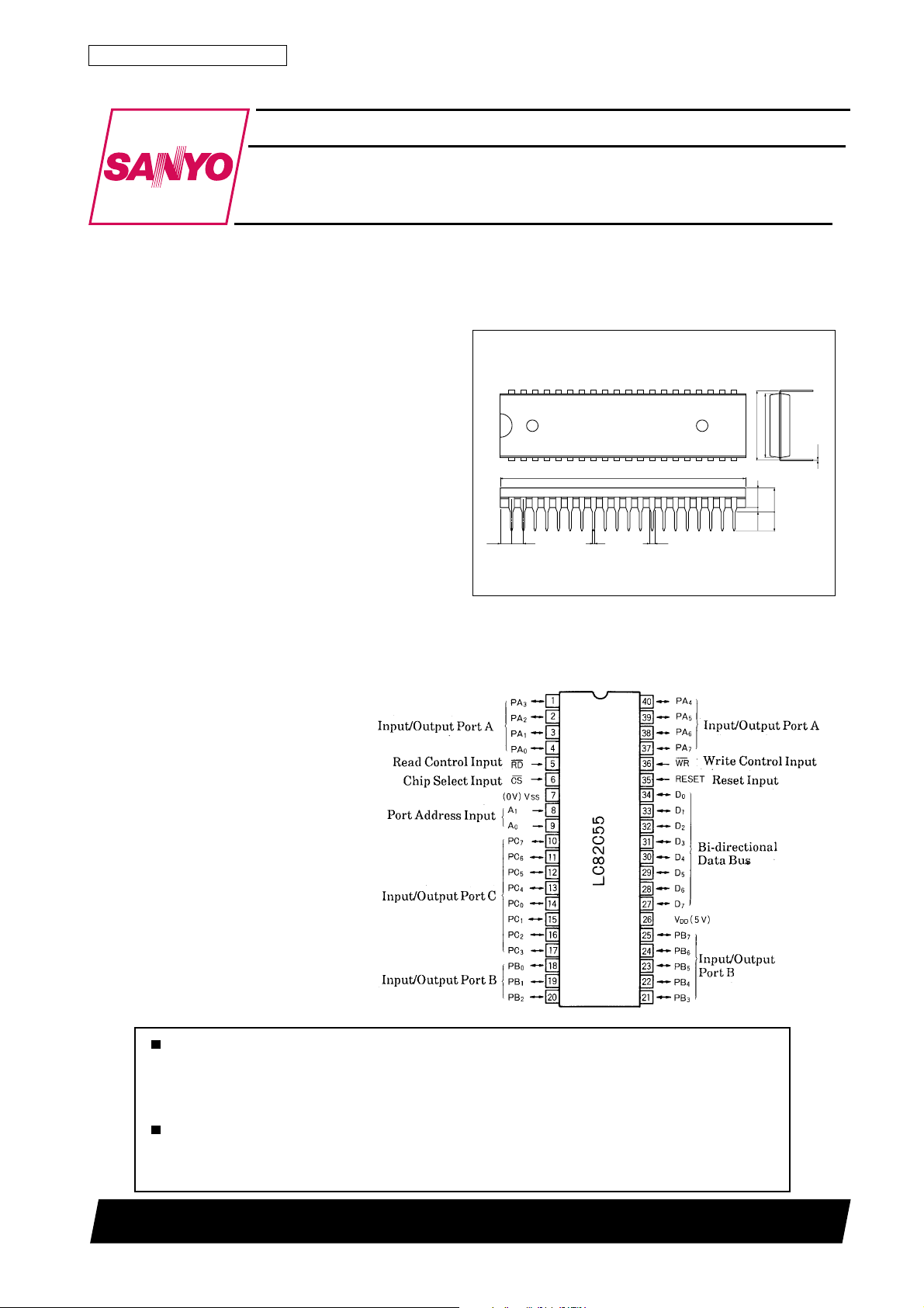
Package Dimensions
unit:mm
3013A-DIP40
[LC82C55]
40
1
2.47 2.54
Pin Assignment (Top view)
53.2
0.5
1.2
21
13.8
15.24
20
4.25
5.2max
4.1
0.51min
SANYO : DIP40
0.25
91001TN (KT)/4058TA,TS No.2721–1/16
Page 2
LC82C55
Specifications
Absolute Maximum Ratings at VSS = 0V
retemaraPlobmySsnoitidnoCsgnitaRtinU
egatlovylppusmumixaMV
egatlovtupnIV
noitapissidrewopelbawollAxamdP 1W
erutarepmetgnitarepOrpoT –57+ot02
erutarepmetegarotSgtsT –051+ot56
DC Recommended Operating Conditions at Ta = –20 to +75˚C, VSS = 0V
retemaraPlobmySsnoitidnoCsgnitaRtinU
egatlovylppuSV
egatlovlevel-woltupnIV
egatlovlevel-hgihtupnIV
Electrical Characteristics(1)
DC Characteristics at Ta = –20 to +75˚C, VDD = 5V ± 10%, VSS = 0V
retemaraPlobmySsnoitidnoC
egatlovlevel-woltuptuOV
egatlovlevel-hgihtuptuOV
tnerrucegakaeltupnII
tnerrucegakaeltaolftuptuOI
)noitarepolamroN(1niardtnerruCI
)edomyb-dnatS(2niardtnerruCI
ecnaticapactupnIC
ecnaticapacnipO/IC
xam –7+ot3.0V
DD
NI
DD
V
LI
V
HI
I
LO
LO
IHO=– Aµ0044.2V
HO
VNIV=
LI
V
LFO
1 01Am
DD
2 01Aµ
DD
NI
f
c
O/I
%01±V5=–8.0+ot3.0V
DD
%01±V5=ot0.2VDD3.0+V
DD
Am5.2= 54.0V
V0ot01±Aµ
DD
V=
TUO
V0ot01±Aµ
DD
–ot3.0VDD3.0+V
˚C
˚C
5.5ot5.4V
sgnitaR
nimpytxam
.V0tadlehsnipderusaemnu,zHM1=
tinU
01Fp
02Fp
Electrical Characteristics(2)
AC Characteristics at Ta = –20 to +75˚C, VDD = 5V ± 10%, VSS = 0V
retemaraPlobmySsnoitidnoC
])elcycdaer(gnimitsuB[
DRerofebelbatssserddA ↓ t
DRretfaelbatssserddA ↑ t
htdiweslupDRt
DRerofebdilavataD ↓ t
DRretfadilavataD ↑ t
evisseccusneewtebemiT
selcycetirw/daeR
])elcycetirw(gnimitsuB[
RWerofebelbatssserddA ↓ t
RWretfaelbatssserddA ↑ t
htdiweslupRWt
RWerofebdilavataD ↑ t
RWretfadilavataD ↑ t
evisseccusneewtebemiT
selcycetirw/daeR
]sgnimitsubrehtO[
RWretfatuptuO ↑ t
DRerofebdilavatadtroP ↓ t
DRretfadilavatadtroP ↑ t
htdiweslupKCAt
htdiweslupBTSt
BTSerofebdilavatadtroP ↓ t
BTSretfadilavatadtroP ↑ t
KCAretfatuptuO ↓ t
KCAretfataolftroP ↑ t
RA
AR
RR
C
DR
FD
t
VR
WA
AW
WW
WD
DW
t
VR
BW
RI
RH
KA
TS
SP
HP
DA
DK
Fp051= 021sn
L
C
C
C
C
R,Fp02=
L
L
L
L
k2= Ω 0158sn
L
Fp051= 053sn
Fp051= 003sn
R,Fp02=
k2= Ω 02052sn
L
sgnitaR
nimpytxam
0sn
0sn
061sn
002sn
0sn
0sn
021sn
001sn
0sn
002sn
0sn
0sn
003sn
053sn
0sn
051sn
Continued on next page.
tinU
No.2721–2/16
Page 3
Continued from preceding page.
retemaraPlobmySsnoitidnoC
RWretfa0=FBO ↑ t
KCAretfa1=FBO ↓ t
BTSretfa1=FBI ↓ t
DRretfa0=FBI ↑ t
DRretfa0=RTNI ↓ t
BTSretfa1=RTNI ↑ t
KCAretfa1=RTNI ↑ t
RWretfa0=RTNI ↓ t
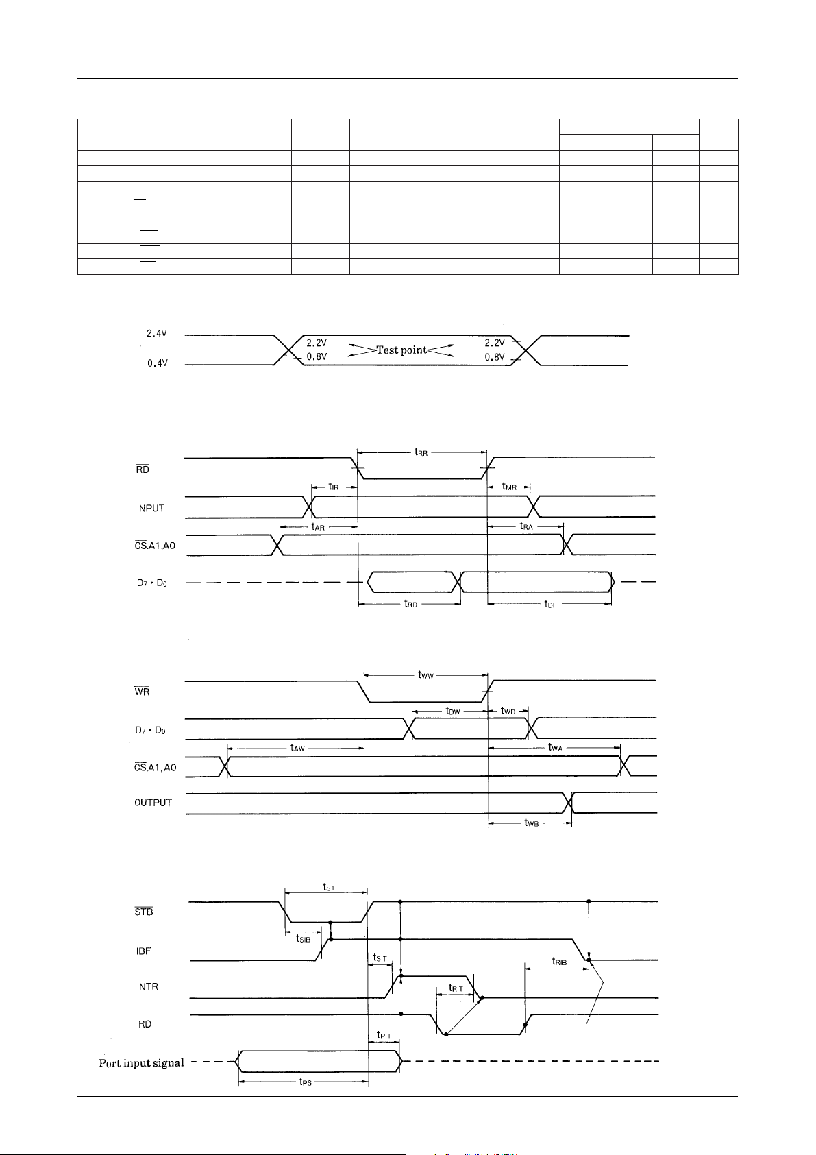
AC Test Input Waveform
Input/Output Waveforms
Mode 0 (Basic Input Mode)
LC82C55
sgnitaR
nimpytxam
C
BOW
BOA
BIS
BIR
TIR
TIS
TIA
TIW
Fp051= 003sn
L
C
Fp051= 053sn
L
C
Fp051= 003sn
L
C
Fp051= 003sn
L
C
Fp051= 004sn
L
C
Fp051= 003sn
L
C
Fp051= 053sn
L
C
Fp051= 054sn
L
tinU
Mode 0 (Basic Output Mode)
Mode 1 (Strobed Input Mode)
No.2721–3/16
Page 4
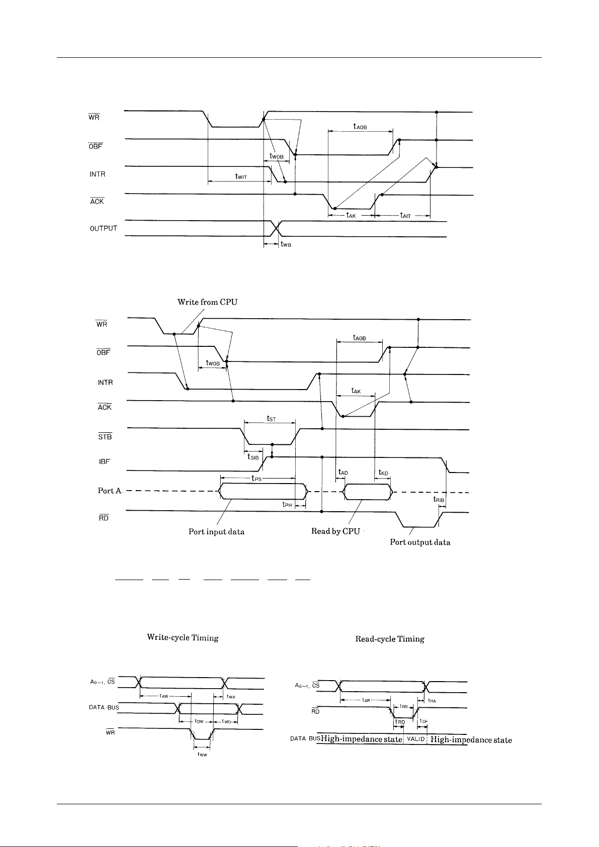
Mode 1 (Strobed Output Mode)
Mode 2 (Bi-directional Bus Mode)
LC82C55
Note
INTR = IBF · MASK · STB · RD + OBF · MASK · ACK · WR
No.2721–4/16
Page 5
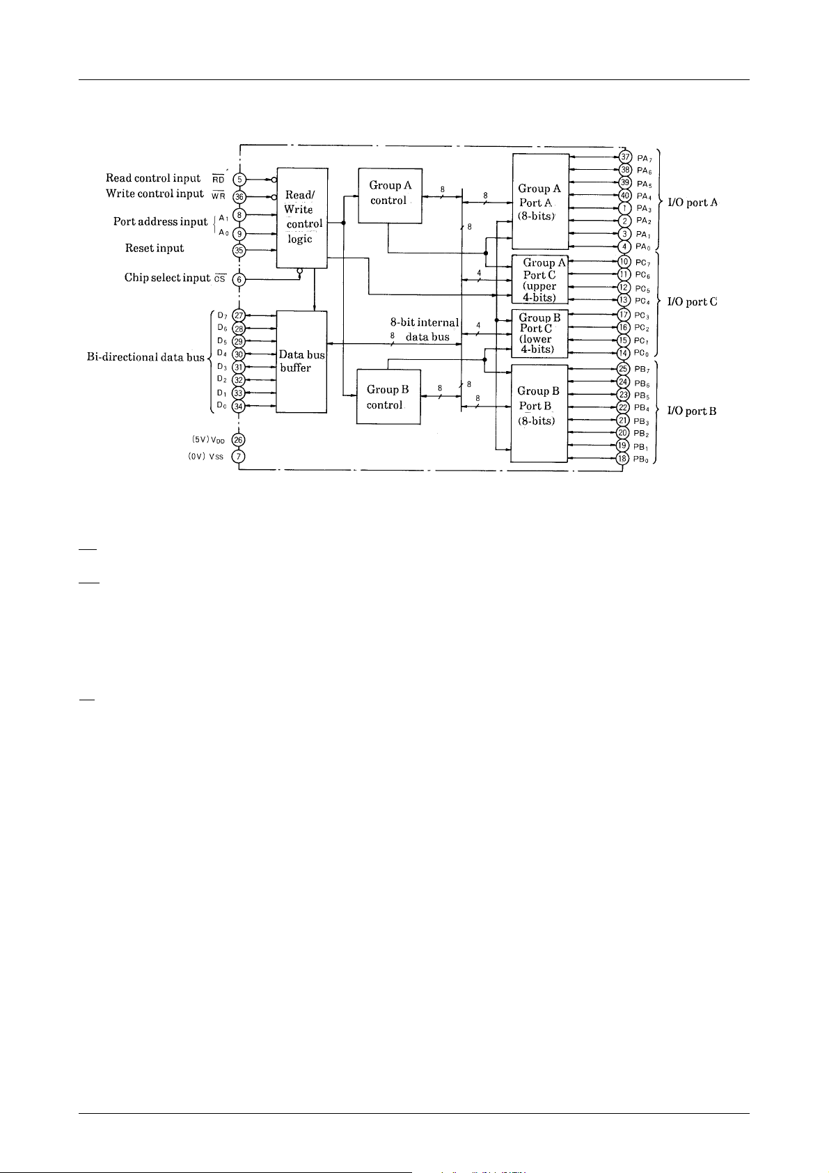
Block Diagram
LC82C55
Description of Operation
RD (read control input)
When Low, data or status word is transferred from the LC82C55 to the CPU via the data bus.
WR (write control input)
When Low, a data or control word is written from the CPU to the LC82C55.
A0, A1 (port address inputs)
Used to select Ports A, B and C, and the control register. Normally, the least significant 2 bits of the address bus are
connected to these pins.
RESET input
A High level on this input clears the control register. All ports are set to the input mode (high-impedance state).
CS (chip select input)
A Low level on this input enables communication between the LC82C55 and CPU . W hen High, the data b us remains in
the high-impedance state and control signals from the CPU are ignored.
Read/write control logic
This block performs the transfer of data and control words between the CPU and the internal circuitry. It receives data
via the CPU interface signals and data bus, and issues commands to the port control logic.
Data bus buffer
This 8-bit, tri-state, bi-directional bus buffer interfaces the external 8-bit data bus to the LC82C55. Data control, and
status information is transferred under the control of the CPU.
Group A/Group B control
Ports A, B and C are divided into the control Groups A and B, each with its own control circuitry. Group A consists of
Port A and the upper 4 bits of Port C; Group B consists of port B and the lower 4-bits of Port C.
The control register is write-only.
Ports A, B and C
The operating mode of each 8-bit port is set by the CPU system software. Port A has an output latch/b uffer and an input
latch.
Port B has an input/output latch/buffer and an input buffer.
Port C has an output latch buffer and input buffer, and can be divided into two 4-bit ports using mode control. Each 4bit port can be used as status and control signals for Ports A and B.
No.2721–5/16
Page 6

LC82C55
Table 1 Basic Operation
A
00001 subataD ← AtroP
01001 subataD ← BtroP
10001 subataD ← CtroP
00010 AtroP ← subataD
01010 BtroP ← subataD
10010 CtroP ← subataD
11010 retsigerlortnoC ← subataD
××
11001 noitarepolagellI
0 : Low-level
1 : High-level
Bit Set/Reset
When Port C is used as an output port, any individual bit can be set or reset with a single control word from the CPU.
This feature simplifies CPU control software in certain applications.
The bit/reset feature of Port C is also used to enable or disable the interrupt request signals from Ports A and B, when
these ports are operating in Modes 1 or 2.
A
1
0
SCDRRWnoitcnuF
1
××
etatsecnadepmi-hgihsisubataD
Figure 1. Port C Bit/Reset Control Word
Basic Operating Modes
The LC82C55 has three basic operating modes, selectable by control words from the CPU.
(1) Mode 0 : Basic input/output
(2) Mode 1 : Strobed input/output
(3) Mode 2 : Bi-directional bus
The operating modes for Groups A and B can be selected independently, however, Mode 2 operation can be selected
for Group A only.
Figure 2 shows the format of the mode selection control word.
No.2721–6/16
Page 7

LC82C55
Figure 2. Mode Set Control Word
1. Mode 0 (basic input/output mode)
Mode 0 is used for simple input/output operations for Ports A, B and C (Port C is used as two, 4-bit ports). There
are no control signals such as interrupt requests or handshaking.
Output data to a port is latched. Input data is not latched.
Each of the two, 8-bit ports and two, 4-bit ports can be used for either input or output.
The I/O configurations for Mode 0 are shown in Figure 3.
Figure 3. Mode 0 Port I/O Configurations
No.2721–7/16
Page 8

LC82C55
2. Mode 1 (strobed input/output mode)
Mode 1 can be selected independently for Groups A and B. Each group consists of an 8-bit data port and a 4-bit
control/data port.
Data is transferred to or from a Mode 1 port with strobes or handshaking signals. Ports A and B provide each
group’s I/O signals, and Port C provides these control signals. Both input and output data are latched.
Input Mode Control Signals
STB (strobe input)
When Low, the data present on the port input pins is loaded into the input latch, STB enables the data from a
peripheral device to be latched into the LC82C55 without CPU intervention.
IBF (input buffer full flag)
A High level on this output indicates that input data has been latched into the LC82C55. This flag is set on the
falling edge of STB and is reset on the rising edge of RD.
INTR (interrupt request output)
This active-high output can be used to interrupt the CPU when input data is strobed into the port. If the interrupt
enable flag, INTE is High, INTR is set on the rising edge of the STB input. INTR is reset on the falling edge of
the RD input.
INTEA and INTEB are set and reset using the bit set/reset capability of Port C. INTEA and INTEB correspond to
Bits 4 and 2, respectively (PC4 and PC2) for Mode 1 input.
Examples of Mode 1 input are shown in Figure 4. The timing waveforms are shown in Figure 5.
Figure 4. Mode 1 Input Configuration Figure 5. Mode 1 Input Timing
Output Mode Control Signals
OBF (output buffer full flag)
This active-low output indicates to a peripheral device that data is available in the port’s output buffer. It is set to
Low by the rising edge of the WR input, and is reset to High by the falling edge of the ACK input.
ACK (acknowledge input)
This active-low input indicates that the peripheral device has accepted data present on the port output.
INTR (interrupt request output)
This active-high output can be used to interrupt the processor when a peripheral devices accepts data from the
LC82C55.
INTR is set if INTE is High (active), and both OBF and ACK are High (inactive). It is reset on the falling edge of
WR.
INTEA and INTEB are set and reset using the bit set/reset capability of Port C. INTEA and INTEB correspond to
Bits 4 and 2, respectively (PC6 and PC2) for Mode 1 output.
Examples of the use of Port A and Port B for input/output in Mode 1 are shown in Figures 8 and 9.
No.2721–8/16
Page 9

LC82C55
Figure 6. Mode 1 Output Configuration Figure 7. Mode 1 Output Timing
Figure 8. Mode 1 Input/Output Example Figure 9. Mode 1 Input/Output Example
3. Mode 2 (strobed bi-directional bus)
Mode 2 provides a single 8-bit bi-directional bus. Handshaking and interrupt signals are available to control the
flow of data between the peripheral device and the LC82C55.
This mode can only be used for Group A. It uses an 8-bit bi-directional data port (Port A) and a 5-bit control port
(upper 5 bits of Port C). Inputs and outputs are both latched. The selection of Group B’s operating mode is independent of Group A’s operating mode.
Mode 2 Control Signals
OBF (output buffer full flag)
This active-low output signal indicates that the CPU has written data to the Port A output buffer.
ACK (acknowledge input)
The tri-state outputs are enabled while the ACK input is Low. When ACK is High, the output drivers are in the
high-impedance state.
STB (strobe input)
When Low, the data present on the Port A pins are loaded into the input latch.
IBF (input buffer full flag)
This active-high output indicates that data has been latched into the Port A input latch.
No.2721–9/16
Page 10

LC82C55
INTR (interrupt request output)
This active-high output signal can be used to interrupt the CPU on both input and output operations. Operation is
the same as in Mode 1.
There are two interrupt request control flags : INTE1 and INTE2.
INTE 1 is combined with OBF and ACKA, to generate an interrupt request on output data transfers. It is controlled
by bit set/reset of DC6.
INTE 2 is combined with IBF and STBA, to generate an interrupt request on input data transfers. It is controlled
by bit set/reset of DC4.
Figure 10. Mode 2 Timing Waveforms
Figure 11. Mode 2 Input/Output Configuration
4. Reading Control Signals
When any of the Port C pins are used as control signals, the CPU can read these signals from Port C. These signals
appear on the data bus as shown in Table 2. Note that the INTE flags are present in place of the STB and ACK
signals. Port C pins not used for control or status are used as normal input or output pins, in accordance with the
Port C input/output mode. Only those pins defined as Mode 0 outputs are affected by a write to Port C. Note that the
INTE flags can only be changed using the appropriate bit set/reset commands.
Table 2. Port Control Signals
ataD
D
edoM
tupni1edoMO/IO/IFBI
tuptuo1edoMFBO
2edoMFBO
7
A
A
D
6
ETNI
A
1ETNIFBI
D
5
A
O/IO/IRTNI
A
D
4
ETNI
A
2ETNIRTNI
D
3
RTNI
A
A
A
D
2
ETNI
B
ETNI
B
ETNI
B
D
FBI
FBO
1
B
B
etoNeeSRTNI
Note
IBFB for 1 input, OBFB for Mode 1 output.
D
0
RTNI
B
RTNI
B
B
No.2721–10/16
Page 11

LC82C55
5. Control Word Tables
Table 3, 4 and 5 summarize the mode definition control words for Modes 0, 1 and 2. Note that the operating modes
for both control groups can be set independently, however, these options have not been included in Tables 3 and 4.
Table 6 summarizes the bit set/reset control words.
Table 3. Mode 0 Control Words
droWlortnoCApuorGBpuorG
D7D6D5D4D3D2D1D
10000000 08TUOTUOTUOTUO
10000001 18TUOTUONITUO
10000010 28TUOTUOTUONI
10000011 38TUOTUONINI
10001000 88TUONITUOTUO
10001001 98TUONINITUO
10001010 A8TUONITUONI
10001011 B8TUONININI
10010000 09NITUOTUOTUO
10010001 19NITUONITUO
10010010 29NITUOTUONI
10010011 39NITUONINI
10011000 89NINITUOTUO
10011001 99NININITUO
10011010 A9NINITUONI
10011011 B9NINININI
0
-axeH
lamiced
AtroP
CtroP
)stib4reppU(
CtroP
)stib4rewoL(
BtroP
droWlortnoCApuorGBpuorG
D7D6D5D4D3D2D1D
10 100 10
10 100 11
10 10 110
10 10 111
10 110 10
10 110 11
1011110
1011111
droWlortnoCApuorGBpuorG
D7D6D5D4D3D2D1D
11
11
11
11
11
11
×××
×××
×××
×××
×××
×××
000 0C
001 1C
010 2C
011 3C
10
11
Table 4. Mode 1 Control Words
0
×
×
×
×
×
×
×
×
-axeH
lamiced
4A
5A
5A
7A
CA
DA
EA
FA
4B
5B
6B
7B
CB
DB
EB
FB
AtroP
CP
TUOFBO
TUOFBO
TUOFBO
TUOFBO
NITUOFBI
NITUOFBI
NINIFBI
NINIFBI
CP
7
6
KCA
A
KCA
A
KCA
A
KCA
A
CtroPCtroP
CP
CP
5
4
A
A
A
A
TUORTNI
TUORTNI
NIRTNI
NIRTNI
A
A
A
A
BTS
A
BTS
A
BTS
A
BTS
A
CP
CP
3
A
A
A
A
RTNI
A
RTNI
A
RTNI
A
RTNI
A
CP
2
KCA
B
BTS
B
KCA
B
BTS
B
KCA
B
BTS
B
KCA
B
BTS
B
CP
1
0
FBO
FBI
FBO
FBI
FBO
FBI
FBO
FBI
RTNI
B
RTNI
B
RTNI
B
RTNI
B
RTNI
B
RTNI
B
RTNI
B
RTNI
B
BtroP
TUO
B
NI
B
TUO
B
NI
B
TUO
B
NI
B
TUO
B
NI
B
Table 5. Mode 2 Control Words
0
×
×
-axeH
lamiced
4C
6C
AtroP
CP
CP
7
→←
→←
→←
→←
→←
→←
FBO
FBO
FBO
FBO
FBO
FBO
6
KCA
A
KCA
A
KCA
A
KCA
A
KCA
A
KCA
A
CtroPCtroP
CP
CP
5
FBI
A
FBI
A
FBI
A
FBI
A
FBI
A
FBI
A
4
BTS
A
A
A
A
A
A
A
BTS
A
BTS
A
BTS
A
BTS
A
BTS
A
CP
CP
CP
3
RTNI
RTNI
RTNI
RTNI
RTNI
RTNI
2
A
A
A
A
KCA
A
B
BTS
A
B
CP
1
NITUO
NINI
FBO
FBI
0
TUOTUO
TUONI
RTNI
B
RTNI
B
BtroP
TUO
B
NI
B
No.2721–11/16
Page 12

LC82C55
Table 6. Control Words for Port C Bit Set/Reset
droWlortnoCCtroP
D7D6D5D4D3D2D1D
×××
0
×××
0
×××
0
×××
0
×××
0
×××
0
×××
0
×××
0
×××
0
×××
0
×××
0
×××
0
×××
0
×××
0
×××
0
×××
0
0000 000
0001 101
0010 200
0011 301
0100 400
0101 501
0110 600
0111 701
1000 800
1001 901
10 10 A00
10 11 B01
1100 C00
1101 D01
1110 E00
1111 F01
0
-axeH
CP
7CP6CP5CP4CP3CP2CP1CP0
lamiced
Sample Application Circuit
1. Mode 0
A typical Mode 0 application circuit is shown in Figure 12. This circuit has 8 input pins and 16 output pins. The CPU
used is the 8085.
skrameR
ETNI:tupnI1edoM
B
ETNI:tuptuO1edoM
B
ETNI:tupnI1edoM
A
ETNI:2edoM
2
ETNI:2edoM
1
teser/tes
ETNI:tuptuO1edoM
A
teser/tes
teser/tes
teser/tes
teser/tes
teser/tes
Figure 12. Mode 0 Application Circuit
No.2721–12/16
Page 13

LC82C55
The control word for this particular input/output configuration is 10010000 (90H). The PPI is initialized by the
following 8085 instructions:
MVI A, 90H
OUT 03H
The instruction sequence for reading data from Port A and writing it to Ports B and C is as follows:
IN 00H Port
OUT 01H Register
OUT 02H Register
The following instruction sequence reads data from Port A, outputs it to Port B, and sets Bit 0 of Port C.
IN 00H Port
OUT 01H Register
MVI A, 01H Control
OUT 03H Output
2. Mode 1
A typical application circuit for Mode 1 is shown in Figure 13.
Figure 13. Mode 1 Application Circuit
The peripheral device can latch data into Port A using the input strobe signal STBA. The input buffer full flag IBFA is set
to High. If interrupt request generation has been enabled by setting the INTEA flag, an interrupt request is generated on
INTRA. For polled operation, the CPU can check the value of the IBFA flag by reading Port C of the LC82C55.
The following program examples demonstrate the use of the Mode 1 application circuit.
MVI A, B0H Control word 10110000. Port A set to input, Ports B and C set to output.
OUT 03H Output to control address
MVI A, 09H Set the INTE flag, 00001001.
OUT 03H Output to control address
EI Enable processor interrupts.
HALT Wait for input data.
When data is strobed into Port A by the STBA signal, the input data is latched into the Port A input buffer. The CPU
transfers control to the RST7.5 interrupt vector (003CH). A typical RST7.5 interrupt service routine is as follows:
ORG 003CH Location set to 003CH
003CH IN 00H Read Port A.
EI Enable Interrupts.
RET Return
No.2721–13/16
Page 14

LC82C55
3. Mode 2
A typical application circuit for Mode 2 is shown in Figure 14. This circuit demonstrates the use of a bi-directional
Mode 2 interface in a master/slave CPU system configuration.
Figure 14. Mode 2 Application Circuit
The LC82C55 is mapped into the I/O address space of the master CPU. The master CPU must initialize Group A to
Mode 2 operation.
The tri-state bi-direcitonal I/O pins of Port A are directly connected to the slave CPU data bus. Additional circuitry is
used to allow the slave CPU to read the LC82C55 IBFA (input buffer full) and OBFA (output buffer full) signals as
Bits 1 and 0 of I/O address 01H. Port A of the LC82C55 is located at I/O address 00H. A read by the slave CPU from
this address activates the ACKA input signal, and data is transferred from Port A to the slave CPU. A write activates
the STBA input signal, causing data from the slave CPU to be loaded into the input latch of Port A.
Both reads from and writes to the LC82C55 by the slave CPU can generate an interrupt to the master CPU via the
LC82C55 INTR output signal. These interrupts are enabled or disabled by setting the appropriate INTE1 and INTE2
flags using the Port C bit set/reset commands.
Data transfer from master CPU to slave CPU
• The slave CPU writes a byte of data to Port A of the LC82C55 (I/O address 00H). IBFA is set to High.
• The master CPU writes a byte of data to Port A of the LC82C55. The OBFA signal goes Low.
• The slave CPU polls the OBFA flag (Bit 0 of I/O address 01N). When OBFA is read as active, the slave CPU reads
the data byte from Port A (I/O address 00H). OBFA returns to High.
• The master CPU polls the status of the OBFA and IBFA flags by reading Port C of the LC82C55. It waits for a High
level on OBFA, indicating that the previous data byte has been read, before writing another byte. The IBFA flag
may also be checked at this time.
Data transfer from slave CPU to the master CPU
• The slave CPU writes a byte of data to Port A of the LC82C55 (I/O address 00H). IBFA is set to High.
• The master CPU checks the status of the IBFA flag by reading Port C of the LC82C55. If High, the master CPU
reads a byte of data from Port A. IBFA is reset to Low.
• The slave CPU polls the IBFA flag (Bit 1 of I/O address 01H). A Low level indicates that the previous data byte has
been read by the master CPU, and another byte can then be written.
The above data transfers operations have not used the INTR signal to interrupt the main CPU. If INTR is used,
polling of the OBFA and IBFA flags by the master CPU is not necessary.
Note that there are separate latches for input and output data. A complete data transfer in one direction does not have
to be completed before a transfer in the opposite direction is initiated.
No.2721–14/16
Page 15

Program examples for the master/slave CPU system.
LC82C55
(1) Master CPU program to transfer
data to the slave CPU.
(3) Slave CPU program to transfer
data to the master CPU.
(2) Master CPU program to receive
data from the slave CPU.
(4) Slave CPU program to receive
data from the master CPU.
4. PPI address decoding
Figures 15 and 16 give examples of address decoding for a system with multiple LC82C55s.
Figures 15 and 16 both perform the same function, since the 8-bit I/O address appears on both the upper and lower
halves of the 8085 address bus during an I/O operation. The example in Figure 15 de-multiplexes the lower half of
the address bus from the data bus, while the Figure 16 example uses the upper half of the address bus.
Figure 15. PPI Address Decoding (1)
Figure 16. PPI Address Decoding (2)
No.2721–15/16
Page 16

LC82C55
5. Initial state of PPI
The LC82C55 must be reset after power up, and the operating mode set. Figure 17 shows the power-up and initialization waveforms when the ports are set to output mode.
Figure 17. PPI Reset On Power-Up
Note
The power-up reset pulse must be at least 50µs long. Subsequent reset pulses must be at least 500ns long.
Specifications of any and all SANYO products described or contained herein stipulate the performance,
characteristics, and functions of the described products in the independent state, and are not guarantees
of the performance, characteristics, and functions of the described products as mounted in the customer's
products or equipment. To verify symptoms and states that cannot be evaluated in an independent device,
the customer should always evaluate and test devices mounted in the customer's products or equipment.
SANYO Electric Co., Ltd. strives to supply high-quality high-reliability products. However, any and all
semiconductor products fail with some probability. It is possible that these probabilistic failures could
give rise to accidents or events that could endanger human lives, that could give rise to smoke or fire,
or that could cause damage to other property. When designing equipment, adopt safety measures so
that these kinds of accidents or events cannot occur. Such measures include but are not limited to protective
circuits and error prevention circuits for safe design, redundant design, and structural design.
In the event that any or all SANYO products(including technical data,services) described or
contained herein are controlled under any of applicable local export control laws and regulations,
such products must not be exported without obtaining the export license from the authorities
concerned in accordance with the above law.
No part of this publication may be reproduced or transmitted in any form or by any means, electronic or
mechanical, including photocopying and recording, or any information storage or retrieval system,
or otherwise, without the prior written permission of SANYO Electric Co. , Ltd.
Any and all information described or contained herein are subject to change without notice due to
product/technology improvement, etc. When designing equipment, refer to the "Delivery Specification"
for the SANYO product that you intend to use.
Information (including circuit diagrams and circuit parameters) herein is for example only ; it is not
guaranteed for volume production. SANYO believes information herein is accurate and reliable, but
no guarantees are made or implied regarding its use or any infringements of intellectual property rights
or other rights of third parties.
This catalog provides information as of September, 2001. Specifications and information herein are
subject to change without notice.
PS No.2721–16/16
 Loading...