

Sanyo LC822964, LC99359, LC99812, LV24000, LV24002 Brochure
...
'06-04
Cell Phone Devices
CONTENTS ⋯⋯⋯⋯⋯⋯⋯⋯⋯⋯⋯⋯⋯⋯⋯⋯⋯⋯⋯⋯⋯3
SANYO Group Cell Phone Components ⋯⋯⋯⋯⋯⋯⋯⋯4
[SANYO Original technology]
Integrated System in Board⋯⋯⋯⋯⋯⋯⋯⋯⋯⋯⋯⋯⋯⋯6
Integrated System in Board Application Products
(Standard Products) ⋯⋯⋯⋯⋯⋯⋯⋯⋯⋯⋯⋯⋯⋯⋯⋯⋯8
Cell Phone Block Diagram Examples⋯⋯⋯⋯⋯⋯⋯⋯⋯10
Frame Transfer Full-Color CCD Sensors ⋯⋯⋯⋯⋯⋯⋯12
1/4-Type 3.2 MP CCD Camera Module for Cell Phones ⋯14
System-on-chip FM Radio ICs for Miniature Cell Phones⋯⋯⋯
16
System-on-chip FM Radio ICs Easy Radio IC
TM
Series ⋯18
Sound Generator IC (MIDI)⋯⋯⋯⋯⋯⋯⋯⋯⋯⋯⋯⋯⋯⋯20
Audio Compression IC ⋯⋯⋯⋯⋯⋯⋯⋯⋯⋯⋯⋯⋯⋯⋯21
Terrestrial Digital One-Segment Chipset ⋯⋯⋯⋯⋯⋯⋯22
Cell Phone Video Drivers ⋯⋯⋯⋯⋯⋯⋯⋯⋯⋯⋯⋯⋯⋯22
NTSC/PAL Video Encoder ⋯⋯⋯⋯⋯⋯⋯⋯⋯⋯⋯⋯⋯⋯23
Earphone Mic Solutions⋯⋯⋯⋯⋯⋯⋯⋯⋯⋯⋯⋯⋯⋯⋯24
LED Driver ICs ⋯⋯⋯⋯⋯⋯⋯⋯⋯⋯⋯⋯⋯⋯⋯⋯⋯⋯⋯26
New Charge Pump ICs ⋯⋯⋯⋯⋯⋯⋯⋯⋯⋯⋯⋯⋯⋯⋯28
Motor Drivers for Cell Phones ⋯⋯⋯⋯⋯⋯⋯⋯⋯⋯⋯⋯30
Amorphous Optical Sensors⋯⋯⋯⋯⋯⋯⋯⋯⋯⋯⋯⋯⋯32
Cell Phone Discrete Devices⋯⋯⋯⋯⋯⋯⋯⋯⋯⋯⋯⋯⋯34
SANYO's Lineup of High-Reliability Discrete Devices ⋯38
CONTENTS
■
Any and all SANYO products described or contained herein do not have
specifications that can handle applications that require extremely high levels of
reliability, such as life-support systems, aircraft's control systems, or other
applications whose failure can be reasonably expected to result in serious
physical and/or material damage. Consult with your SANYO representative
nearest you before using any SANYO products described or contained herein in
such applications.
■
SANYO assumes no responsibility for equipment failures that result from using
products at values that exceed, even momentarily, rated values (such as
maximum ratings, operating condition ranges, or other parameters) listed in
products specifications of any and all SANYO products described or contained
herein.
■
Specifications of any and all SANYO products described or contained herein
stipulate the performance, characteristics, and functions of the described
products in the independent state, and are not guarantees of the performance,
characteristics, and functions of the described products as mounted in the
customer's products or equipment. To verify symptoms and states that cannot be
evaluated in an independent device, the customer should always evaluate and
test devices mounted in the customer's products or equipment.
■
SANYO Electric Co., Ltd. strives to supply high-quality high-reliability products.
However, any and all semiconductor products fail with some probability. It is
possible that these probabilistic failures could give rise to accidents or events
that could endanger human lives, that could give rise to smoke or fire, or that
could cause damage to other property. When designing equipment, adopt safety
measures so that these kinds of accidents or events cannot occur. Such
measures include but are not limited to protective circuits and error prevention
circuits for safe design, redundant design, and structural design.
■
In the event that any or all SANYO products(including technical data, services)
described or contained herein are controlled under any of applicable local export
control laws and regulations, such products must not be exported without
obtaining the export license from the authorities concerned in accordance with
the above law.
■
No part of this publication may be reproduced or transmitted in any form or by
any means, electronic or mechanical, including photocopying and recording, or
any information storage or retrieval system, or otherwise, without the prior written
permission of SANYO Electric Co., Ltd.
■
Any and all information described or contained herein are subject to change
without notice due to product/technology improvement, etc. When designing
Notes on Package Types and Naming
The package names used in this documentation are designed to indicate rough
classification of the packages used, and do not necessarily indicate the formal name of
each individual package.
Refer to the delivery specifications document for the particular product for the package
dimensions figure and the formal name of the package.
SANYO's leading-edge technologies support
advances in portable electronic equipment.
With the increasingly wide adoption of 3G and later cell phone infrastructure,
cell phones are featuring even more advanced and diverse functionality.
The speed with which multimedia functionality is being adopted is increasing,
and that trend is not limited to Japan, but is spreading worldwide.
SANYO has, for the first time in the industry,
adopted a 1/9-type CCD image sensor for cell phones.
SANYO is moving towards the megapixel age in camera cell phones,
starting with the chip size package (CSP).
Furthermore, SANYO continues to contribute to the development
of the cell phone market with efforts such as developing
SANYO's unique Integrated System in Board module technology
that achieves even higher densities and thinner form factors,
developing QVGA OLED displays,
the Easy Radio IC
TM
series that makes it easy
to include a radio receiver in portable equipment,
providing an extensive lineup of motor drivers for zoom,
autofocus, and other functions in cell phone cameras,
and developing power supply ICs for high pixel count CCDs.
Higher pixel counts, further miniaturization, and lower power.
To respond to these market needs
and to provide new areas of added value
for our customers' products,
SANYO uses their subtle technological arts
to expand their lineup of diverse chipsets
and individual devices.
3
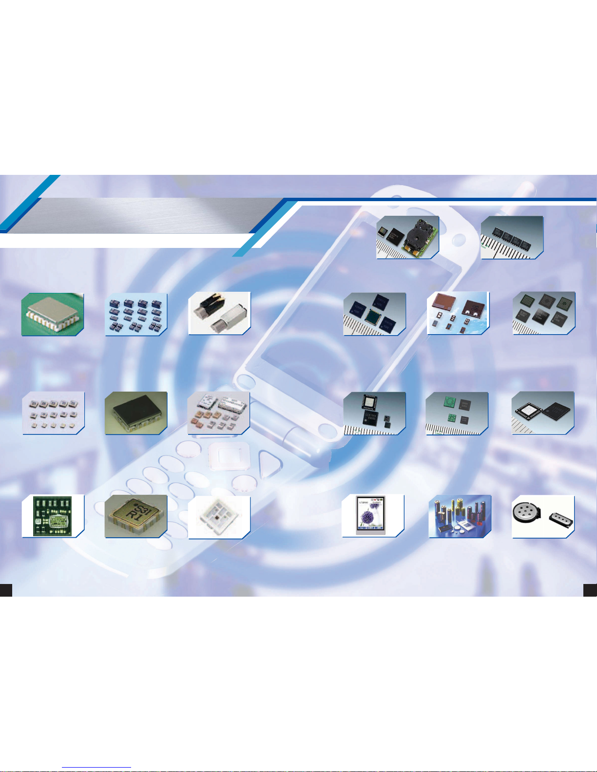
FEM
(Front End Module)
POSCAP
ASM
(Antena Switch
Module)
Integrated
System in Board
SAW Filer
SAW Duplexer
DC/DC
Vibration Motor
Mega Pixel CCD
Camera Module
Speaker
Die Electric Filter
&
Duplexer
RGB Chip LED
Battery
LCD
(SANYO EPSON IMAGING
DEVICES CORPORATION)
Sound Generator
IC
LED Driver
FM Tuner IC
Charge Pump
Amorphous
Optical Sensor
Small discrete
devices
SANYO Group Cell Phone Components
SANYO Group Cell Phone Components
Here we introduce several technologies that SANYO has pushed to the limits.
4 5
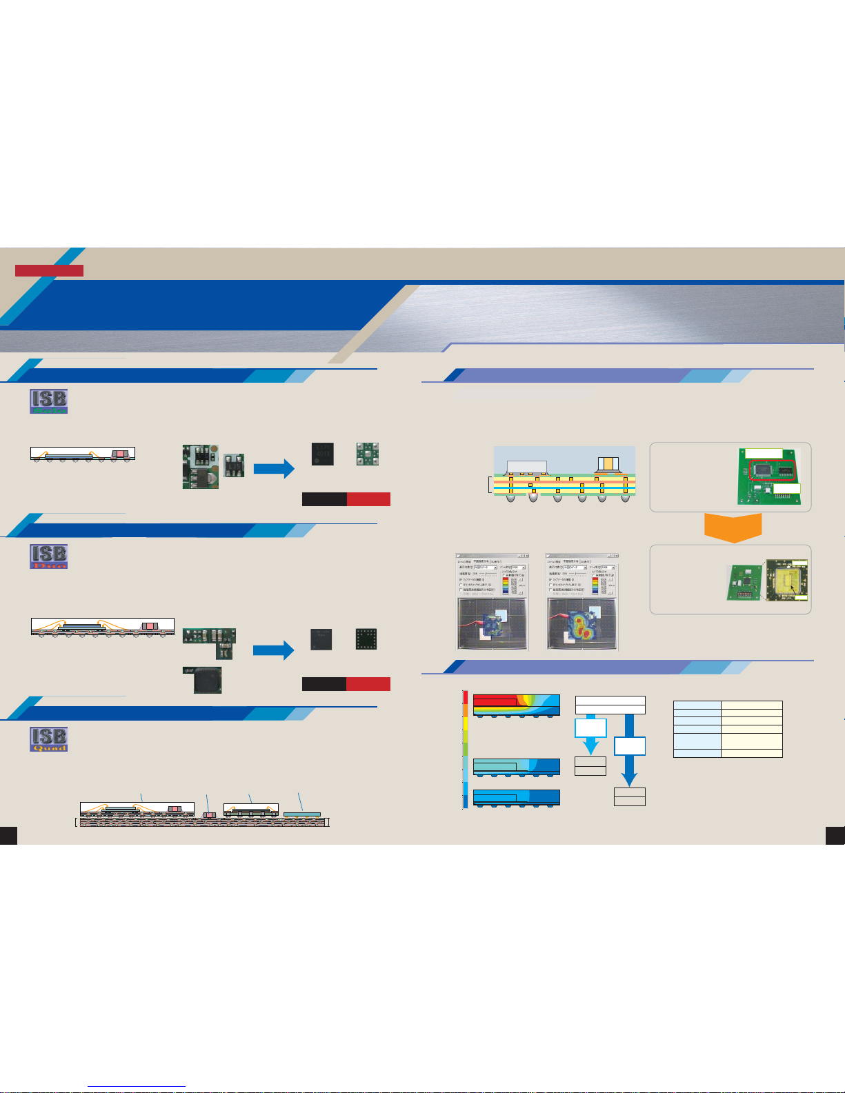
Integrated System in Board is a type of SiP (system in package) technology, and is a module technology that achieves high
densities and thinner form factors by using SANYO's unique substrate and mounting technologies. The Integrated System in
Board lineup consists of three types of process: ISB-Solo, ISB-Duo, and ISB-Quad. Which process is used is selected based on
the application.
In addition to standard products, customer specified circuit blocks can also be converted to Integrated System in Board using an
optimal process, thus creating a new module device in a short time.
76
Integrated System in Board
Integrated System in Board
●Thickness of only 0.45 mm (0.65 mm if resistors are included) realizes excellent thermal radiation and
short development TAT
●Optimal for SiP implementation of small-scale block that includes semi-power semiconductors.
● Adopts unique SANYO-developed 0.2 mm thickness high-density substrate (2 layers)
Line 40
µm / Space 40 µm at 25 µm thickness copper foil,
Via diameter 100 µm / Via land diameter 150 µm
● Thickness of only 0.53 mm (0.73 mm if resistors are included) realizes high-density mounting
● Optimal for SiP implementation of high-frequency (up to 10 GHz) blocks, blocks that require
performance or EMC workarounds based on component placement/wiring pattern, and blocks that
require partial high-density mounting.
●Adopts unique SANYO-developed 0.24 mm thickness high-density substrate (4 layers)
●Thickness of only 0.6 mm realizes high-density mounting
●Optimal for SiP implementation of high-frequency (up to 10 GHz) blocks, blocks that require performance
or EMC workarounds based on component placement /wiring pattern, and subsystems that require highdensity mounting.
●Chip-on-Board type
■ Assembly structure examples
Integrated System in Board
Earlier mounting
Integrated System in Board
Top surface
Back surface
Mounting area
reduced by 80%
4.45 × 4.45 × 0.65 mm
3
Integrated System in Board
Earlier mounting
Integrated System in Board
Top surface
Back surface
Mounting area
reduced by 58%
4.3 × 4.3 × 0.73 mm
3
Passive components
(resistors and capacitors)
ISB-Duo
ISB-Quad
WS-CSP Flip Chip
0.24 mm
■ Application example (Cell phone charger circuit block)
■ Application example (Clock detector block)
■ Assembly structure examples
■ Assembly structure examples
● Reduced wiring area due to implementation as miniature modules
● Integration of noise reducing components
● Supply voltage stabilization by using dedicated layers for power supply and ground
Dedicated power
supply/ground layer
Integration of noise
reducing components
LSI
Analysis conditions
Chip heat generation
Chip size
Land size
Atmospheric temperature
Cooling conditions
Analysis model
3 [W]
4✕4✕0.3 [mm
3
]
5✕5✕0.03 [mm
3
]
25 [°C]
Ideal cooling of the solder lower
surface;
25 [°C]
1/4 model (since symmetrical)
Maximum
temperature
40.4 [°C]
Maximum
temperature
54.3 [°C]
Maximum temperature
92.7 [°C]
Temperature
difference
38.4°C
Temperature
difference
52.3°C
MK
Z
Y X
MK
Z
X
Y
MK
X
Y
97
81
65
49
33
89
73
57
41
25
Typical BGA
Integrated System Board
that dissipates heat
Integrated System Board package
Integrated System in Board Process Lineup
ISB-Solo
ISB-Duo
ISB-Quad
Noise suppression effect (measured)
Heat dissipation effect (simulation)
Module technologies that achieve high-density and thinner form factors
SANYO Original technology
■ Evaluation results using a microcontroller and SRAM
(Surface probe method - 30 MHz to 1 GHz)
SRAM
10 mm × 10 mm
SRAM
Noise is reduced
significantly
Microcontroller
Microcontroller
Wiring on board
Integration of noise
reducing components
Integrated System in
Board stack structure
(high-density mounting)
Integration of noise
reducing components
Reasons noise can be reduced by Integrated Sysytem in Board
ISB-Duo (2-layer ISB)
Separate microcontroller
and SRAM
Surface scan using a field probe
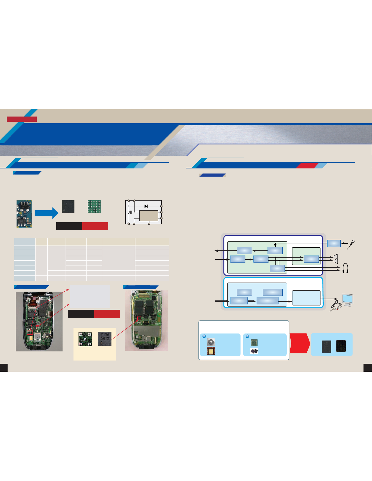
Here we introduce examples of ICs used for cell phones implemented as modules using Integrated System in Board.
These products combine a step-up DC/DC converter, n-channel power MOSFET, and Schottky barrier diode devices
in a single module. A switching step-up power supply can easily be implemented with just the addition of external
voltage setting resistor, coil, and capacitor components.
8 9
Module technologies that achieve high-density and thinner form factors
Integrated System in Board Application
Products (Standard Products)
Integrated System in Board Application
Products (Standard Products)
Top surface
Back surface
3.4 × 3.4 × 0.65 mm
3
Mounting area
reduced by 35%
Earlier mounting
Integrated System in Board
Integrated System in Board
Di
TR
GND
CE
EXT
IC
VDD
FB
■ Block Diagram (SR10010)
■ Block Diagram
■
Compared to discrete components with Integrated System in Board
Type No. Type
Size Status
SR10010 1ch Step-up type 180 kHz 20 V ES samples/MP support
SR10020 300 kHz 20 V ES samples/MP support
SR10030 180 kHz 30 V 3.4 × 3.4 × 0.65 mm
3
ES samples/MP support
SR10110 100 kHz 20 V In volume production
SR10210 100 kHz 20 V In volume production
SR103XX -------- -------- -------- Under development
SR20010 2ch 180 kHz 20 V 5.0 × 5.0 × 0.65 mm
3
ES samples/MP support
Number of
channels
Oscillator
frequency
Withstand
voltage
Step-down
type
– power
supply type
■ Product lineup
2002
2004
Charge control circuit
10.0 × 10.0 = 100.0 mm
2
+
Regurator IC
3.0 × 3.0 = 9.0 mm
2
ISB-E17-0
4.4 5 × 4.45 = 19.80 mm
2
Mounting area
reduced by 80%
Size: 109.0 mm2→ 19.80 mm
2
Thin Form, Miniature 1 or 2 Channel DC/DC Converter Power Supplies
SR Series
Earlier mounted
Integrated system in Board
NTSC/PAL encoder+Video driver+Audio codec+Speaker amplifier
LC822964
■Video Block
●One output system
Low-cost version specialized for cell phones
●Supports a wide variety of input data (ITU-R601/SQ)
●No output coupling capacitors required
●High performance
- Switching noise does not appear on the screen due to
the use of charge pump technology
- Voltage sag does not occur
●Built-in 6th order low-pass filter: fc = 7.5 MHz
●Standby mode power consumption: 0 µA
■Audio Block
●D/A converter signal-to-noise ratio: 98 dB (A
weighting), THD: 84 dB at 48 kHz
●A/D converter signal-to-noise ratio: 90 dB (A
weighting), THD: 80 dB at 48 kHz
●Programmable ALC/noise gate
●Stereo/monaural microphone interface
●Built-in headphone driver
●Low power consumption
●450 mW output (Vcc = 3.6 V, 1 kHz, THD = 1%)
●Power saving and standby functions
Featuring
Speaker
amplifier
Microphone
amplifier
Speaker amplifier
LA74220C
Audio Codec
ALC
ADC
DAC
Volume
Heaphone
amplifier
Audio I/O block
I2S
75 Ω Video Driver
LA73074C
NTSC/PAL Encoder LC822962
Timing
Generator
IIC I/F
ITU-R601/SQ
I/F
NTSC/PAL
Video Encoder
TV output block
CCIR601
Composit
video output
Current mounting area
84.88 mm
2
+
Passive components
Integrated System in Board
45 mm
2
(6.0×7.5 mm
2
)
Sound I/O + TV output
NTSC/PAL encoder
5.0×5.0×1.0 mm
3
Video driver
2.8×2.8×0.8 mm
3
TV Output Block
Sound I/O Block
Audio codec
5.2×5.2×0.8 mm
3
Speaker amplifier
5.0×5.0×0.8 mm
3
Mounting area
can be
reduced by
over 50%
New
product
SANYO Original technology

Since the next generation of cell phones will include an even wider variety of functions than ever before, we expect that
dedicated multimedia processors and devices will be required.
SANYO provides a wide range of devices required by next generation cell phones, and can provide powerful support for your
cell phone development efforts.
携帯電話ブロックダイアグラム例
SANYO devices support megapixel class cameras and provide extensive functionality
Cell Phone Block Diagram Examples
RF
One-segment tuner
Frequency
conversion
Video driver
TV
LCD
display
SP
MIC
LED driver
KEY
Audio
compression
decoder
Sound
generator
Terrestrial
broadcast
one-segment
OFDM
demodulator
FM/AM tuner
Baseband processor
(CPU)
Amorphous
optical
sensors
Flash
memory
External
memory
Graphic
memory
Memory
Power supply
control
Battery
Display
controller
NTSC/PAL
encoder
Application processor
Motor driver
(Miniature series)
Autofocus
Optical zoom
Megapixel CCD
camera module
Sub-camera
CIF/VGA
Charge pump
Charge pump
Integrated System in Board
Audio
codec
Headphone
Diversity antenna
10 11
*: A separate coil is required for applications that include an AM radio
LED Driver
LV5202PL
13-ch 9-LED
driver
High-Efficiency Charge Pump Type
LC410592
7 LEDs
For main LCD backlights
LC410591
LV5203FN
13-ch 11-
LED driver
LV5204PL
13-ch 11-LED
driver
LV5213LP
3-ch RGB-LED
driver
Earphone/Microphone
Solutions
S.T.F.D.
SANYO has developed a chip that
supports communication with just an
earphone.
● Conversation is possible even without
a microphone
● Achieves clearly audible conversation
even in noisy environments
(Single Transducer Full Duplex)
MP3 and WMA Decoder IC
LC823231
By using dedicated circuits with a
hardwired structure to implement
the MP3 and WMA decode
functions, these ICs achieve
extremely low power levels.
(FM+RDS)
LV24010
(FM+source selector+
headphone amplifier)
LV24003
(FM+AM)
These revolutionary devices are
self-contained FM radio ICs that
require no external components.
LV24100
LV24020
These ICs can generate up to 128
sounds at the same time and include
3D Audio functions.
This is the latest sound generator IC
that even supports new melody formats
such as Mobile XMF, and provides the
highest functionality in the series as an
independent sound generator product.
64 or 128-Voice Polyphony
Sound Generator IC Series
Sound Generator +
Audio Compression IC
LC823872
These ICs can generate up to 64
sounds at the same time and
include 3D Audio functions.
This is a combined product that
integrates ultralow-power MP3 and
AAC decoder functions, and is
optimal for use in cell phones for
true audio aficionados.
LC823553
This model corresponds to a low-price
version of the LC823553 with certain
functions removed, and is a combined
product that integrates an ultralowpower MP3 decoder with a sound
generator IC that supports 64-voice
polyphony.
LC823501
Cell Phone 1/4-Type 3.2 MP CCD
Camera Chipset
The extensive depth of field provided
by these camera modules means the
user never has to worry about focus.
These camera modules are optimal for
camera cell phones that need to
provide easy and convenient imaging.
Cell Phone 1/7-Type VGA
Resolution CCD Camera Chipset
These camera modules are optimal for
low-end camera cell phones. These
ultraminiature camera modules are so
small that they do not interfere with the
design of cell phone.
These modules are optimal for
sub-camera of video conferencing
cell phone products.
Cell Phone 1/9-Type CIF
Resolution CCD Camera Chipset
LC99267(CCD)+
LC99807(DSP)
LC99359(CCD)+
LC99812(DSP)
LC99268(CCD)+
LC99809(DSP)
NTSC/PAL Encoder
The cell phone display can easily
be connected to a TV for viewing.
These devices support a wide
variety of input data rates (ITUR601/SQ).
The LC822971 includes 16 Mbits of
SDRAM and allows the CPU to
draw graphics without concern for
the TV display rate.
LC822963
LC822971
LC822961
Video Driver
LA73074CL
Terrestrial Broadcast One-Segment
Frequency Conversion IC
LA8101
The adoption of direct conversion
technology obviates the need for a
SAW filter and supports miniaturization.
Terrestrial Broadcast One-Segment
OFDM Demodulator IC
LC74112
The adoption of diversity synthesis
technology makes stable reception
possible.
4 LEDs
P26, P27
P21
P20
P20
P32, P33
P22
P8, P9
P28, P29
P24
P9
P16 to P19
MP3/AAC/AAC+Decoder
LC82335X
P12 to P15
P23
P22
Under
development
New
product
New
product
Under
development
Under
development
New
product
New
product
New
product
Under
development
Under
development
New
product
New
product
New
product
Under
development
New
product
New
product
Under
development
New
product
Under
development
New
product
Under
development
Under
development
1-Chip FM/AM Tuner ICs
Integrated Audio/Video ICs
LC822964
Integration of an NTSC/PAL
encoder, video drivers, an audio
codec, and a speaker amplifier IC
in a single package using ISB
technology. The mounting area can
be reduced by 50% or more.
Ultraminiature Package 2-Phase
Stepping Motor Drivers
LB1935CL
LB1935T
LB1906CL
Constant Current Driving Motor Driver with
1-ch H Bridge and Thermal Shutdown Curcuit
LB1941T
LB1941CL
2-ch stepping + 1-ch Constant Current
Forward/Reverse Motor Driver IC
LB8682CL
1-ch Low-Saturation
Forward/Reverse Motor Driver
LB1938T
2-Phase Excitation Motor Driver
LB1801CL
1.5-ch Constant Current
Forward/Reverse Motor Driver IC
LB8683CL
Auto Foucus Piezo Actuator
LV8071LG
P30, P31
New
product
Under
development
Under
development
SANYO fabricates frame transfer (FT) CCD sensors using unique technologies with ultrafine design rules and provides them as
modules assembled using advanced leading-edge mounting technologies.
SANYO makes a point of providing fine and delicate semiconductor devices in forms that our customers will find approachable
and easy to use.
1312
High image quality, ultraminiature size, and low power makes these devices optimal for
use in cell phones
Frame Transfer Full-Color CCD Sensors
Achieves the industry’s smallest optical size class by using the frame transfer CCD, which makes it possible to reduce
feature sizes while maintaining sensitivity.
Sensitivity was increased by adopting a simple single-layer gate gap structure and thin-film polysilicon.
Photo Diode
Micro Lens
Photo Diode
Micro Lens
P-Sub
N+ N+P+ P+N+ N+
Micro Lens
Photo Diode
[storage 1/3 compression Type]
Imaging area
Storage area
Horizontal shift register
output
PD
=Transfer
area
Low voltage
Imaging area
Horizontal shift register
output
High voltage
Transfer
area
Switch
PD
Low voltage
X direction register
Y direction register
PD
Amplifier
PD: Photo Diode
FT-CCD CMOS IL-CCD
A charge pump type voltage step-up circuit that features minimal noise generation, and the supply voltages required for
system drive are generated efficiently with just the supply of a single +2.9 V power supply. This design is also effective at
achieving reduced power consumption.
SANYO implemented, in a single package, the timing generator circuit required for system drive and all the analog and
digital processing required to accept the CCD output by taking advantage of the SANYO CMOS analog/digital hybrid
process and MCP (multi-chip package) technologies.
CCD sensor CMOS sensor (1/4 VGA)
2004 2005 2006
Megapixel
CCD chipset
1.0M
VGA CCD
chipset
Coexistance
between
near infrared
sensitivity and
color
3.2M
CIF CCD
chipset
Near infrared
CCD chipset
30 fps
High reliability
LC99807
LC99808
LC99117
LC99268
LC99267
LC99810
LC99353
LC99812
LC99359
LC99704
LC99268G
LC99809
LC99268FL
Near infrared
High image quality
Dynamic range of
VGA motion picture
and 3.2-MP still picture
has expanded
Inproved stability
at high-temperature
(85 °C)
Still Motion Still Motion Motion
Motion
Motion
LC99359 3.2M VGA Low High Normal 30 DigitalColor
LC99268FL VGA VGA High
Wide 15 DigitalColor
LC99117 CIF CIF
Very High
Wide 30 DigitalB&W
Dynamic Range
Frame Rate
Output
Resolution
Sensitivity
Color/B&W
Chip Set
Correlated double
sampling
CCD driver
Charge pump
Power supply circuit
Digital color signal processor
RGB/YUV output
Multifunction DSP
CCD module
CCD timing generator
+2.9 V
Single power supply
Storage area
Imaging area
Horizontal shift
register
Output
amplifier
AGC
8-bit
ADC
Analog front end processor
Registers for picture arrangement
/Output mode/etc.
I
2
C bus
AE/AWB controller
CLK
HREF/VREF
High sensitivity
Horizontal transfer
FT-CCD structure
Mixing area
2R+G B+2G
R, G, and B are extracted by calculations
Compressed to 1/3 the number of lines by combining 3 pixels.
R+2G 2B+G
Low moire
Imaging area
Imaging area
Storage area
Storage area
Mixing area
Frame Transfer CCD
CCD drive circuit and image processing implemented in a single package
Multifunction DSP chip
Device Density Comparison
Roadmap
Cross Section Comparison
Newly developed
Comparison of Differences in Electronic Shutter Types
CCD Module Basic Structure Example
Comparison of chip
sizes required to
acquire the same
imaging device area
The FT CCD method uses
no elements that block the
entrance of light, and thus
they can capture light from
a wider range of incidence
angles.
High sensitivity
Reducing the device
height is possible
In the 1.0-MP CCD, SANYO developed a new charge accumulation method.
Low moire, high sensitivity, and a high frame rate achieved by pixel addition during preview and spatial
filter processing.
 Loading...