

Page 1
Any and all SANYO products described or contained herein do not have specifications that can handle
applications that require extremely high levels of reliability, such as life-support systems, aircraft’s
control systems, or other applications whose failure can be reasonably expected to result in serious
physical and/or material damage. Consult with your SANYO representative nearest you before using
any SANYO products described or contained herein in such applications.
SANYO assumes no responsibility for equipment failures that result from using products at values that
exceed, even momentarily, rated values (such as maximum ratings, operating condition ranges,or other
parameters) listed in products specifications of any and all SANYO products described or contained
herein.
CMOS IC
Image Data Compression/Expansion Processor
Ordering number:ENN*4605
LC8213
SANYO Electric Co.,Ltd. Semiconductor Company
TOKYO OFFICE Tokyo Bldg., 1-10, 1 Chome, Ueno, Taito-ku, TOKYO, 110-8534 JAPAN
Overview
The LC8213 is an IC that compresses (codes) and expands
(decodes) binary image data used for facsimiles, etc. This
LC8213 can be used in office automation equipment such
as G3/G4 facsimiles, image file systems, digital photocopiers, and workstations.
The coding method is based on the MH (Modified
Huffman), MR (Modified Relative Element Address Designate), and MMR (Modified MR) coding methods regulated by CCITT T.4 and T.6.
Features
• CCITT T.4 and T.6 MH, MR, MMR coding methods.
• Compatible with G3 and G4 facsimiles.
• No. of main scanning direction pixels Max. 64k bits.
• Line skip mode.
• 8/16 bit image memory bus, 8-bit CPU bus.
• Transfer of data between CPU bus and image memory
bus.
• DMA transfer function between image memory and I/O
device.
• System clock Max. 20MHz.
• CMOS low power dissipation.
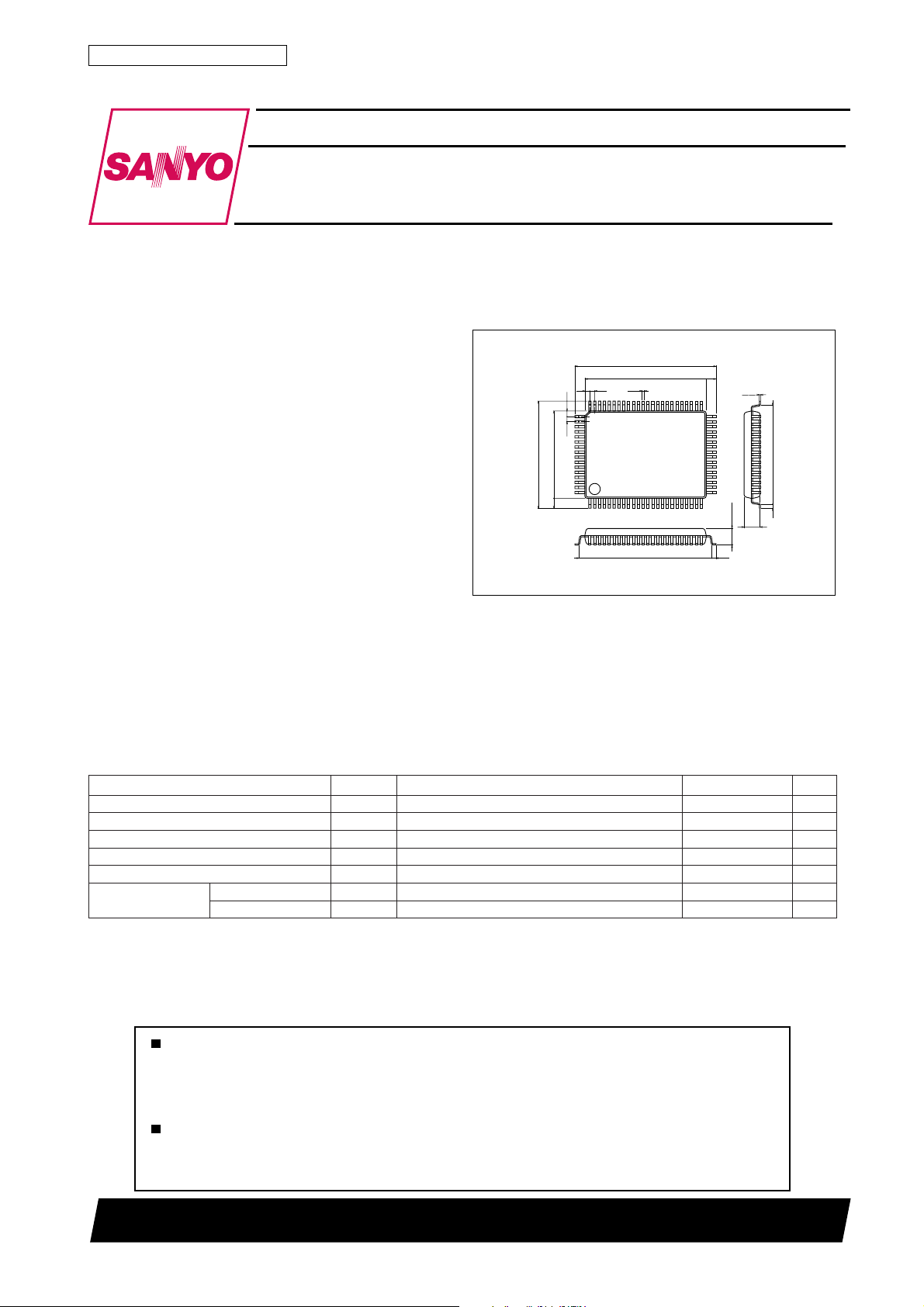
Package Dimensions
unit:mm
3174-QIP80E
[LC8213]
23.2
0.35
20.0
21.6
17.2
0.8 0.8
1.0
64
65
0.8
14.0
80
1.6
124
1.6
0.15
41
40
25
3.0max
2.7
0.8
SANYO : QIP80E
15.6
0.8
Specifications
Absolute Maximum Ratings at Ta = 25˚C, VSS = 0V
retemaraPlobmySsnoitidnoCsgnitaRtinU
egatlovylppusmumixaMV
egatlovtuptuo/tupnIV
noitapissidrewopelbawollAxamdPaT ≤ 07°C 053Wm
erutarepmetgnitarepOrpoT –07+ot03
erutarepmetegarotSgtsT –521+ot55
tsniagaecnatsiseR
taehredlos
redloslaunaMsdnoces3 053
wolfeRsdnoces01 532
xam –0.7+ot3.0V
DD
IV,O
80101TN (KT)/82093JN (KOTO) No.4605–1/10
–Vot3.0
3.0+V
DD
˚C
˚C
˚C
˚C
Page 2
LC8213
Allowable Operating Ranges at Ta = –30 to +70˚C, VSS = 0V
retemaraPlobmySsnoitidnoC
egatlovylppuSV
egnaregatlovtupnIV
DC Characteristics at Ta = –30 to +70˚C, VSS = 0V, VDD = 4.5 to 5.5V
retemaraPlobmySsnoitidnoC
egatlovlevel-hgihtupnIV
egatlovlevel-woltupnIV
tnerrucegakaeltupnII
egatlovlevel-hgihtuptuOV
egatlovlevel-woltuptuOV
tnerrucegakaeltuptuOI
ycneuqerfnoitallicsOf
tnerrucylppuSI
AC Characteristics Clock Reset Timing
retemaraPlobmySsnoitidnoC
emitelcyckcolCKLCt05sn
htdiwlevel-wolkcolCLKCt51sn
htdiwlevel-hgihkcolCHKCt51sn
htdiweslupteseRWTSRtKLCt6sn
DD
NI
HI
LI
VNIV=SSV,
L
IHO=– Am34.2V
HO
I
LO
LO
ZO
DD
KLC 02zHM
CSO
elbitapmocLTT2.2V
elbitapmocLTT 8.0V
DD
Am3= 4.0V
sgnitaR
nimpytxam
5.40.55.5V
0V
sgnitaR
nimpytxam
–5252+Aµ
tuptuoecnadepmihgihgniruD–001001+Aµ
5103Am
sgnitaR
nimpytxam
DD
tinU
V
tinU
tinU
CPU Interface
emitdlohKCADHADt01sn
retemaraPlobmySsnoitidnoC
emitputessserddASAt02sn
emitdlohsserddAHAt01sn
htdiweslupdaeRWRt001sn
emityaledataddaeRDRt 001sn
emitdlohataddaeRHRt01sn
htdiweslupetirWWWt001sn
emitputesatadetirWSDt02sn
emitdlohatadetirWHWt01sn
emitputesKCADSADt02sn
emityaledQERDQRDt
nimpytxam
sgnitaR
07+KLCt2
tinU
sn
No.4605–2/10
Page 3
LC8213
Image Memory Interface
retemaraPlobmySsnoitidnoC
NEA ↓ emityaledLEAt 07sn
NEA ↑ emityaledHEAt 07sn
TSA ↑ emityaledHSAt 07sn
TSA ↓ emityaledLSAt 07sn
emityaleddilavlangislortnoCVWRt 07sn
emityaleddilavnilangislortnoCHWRt 07sn
DROI,DRM ↓ emityaledLDRt 07sn
DROI,DRM ↑ emityaledHDRt 07sn
RWOI,RWM ↓ emityaledLRWt 07sn
RWOI,RWM ↑ emityaledHRWt 07sn
EDL,EDU ↓ emityaledLEDt 07sn
EDL,EDU ↑ emityaledHEDt 07sn
NEDM ↓ emityaledLDMt 07sn
NEDM ↑ emityaledHDMt 07sn
emityaleddilavsserddAVAMt 001sn
emitdlohsserddAHAMt52sn
emitputesataddaeRRSDt01sn
emitdlohataddaeRRHDt0sn
emityaledatadetirWWDDt 08sn
emitdlohatadetirWWHDt01sn
QERB ↑ QERDIrof(emityaled ↑ )HRBt
QERB ↓ emityaledLRBt
KCADI ↓ KCABrof(emityaled ↓ )DCADt
KCADI ↓ KLCrof(emityaled ↑ )LCADt 07sn
KCADI ↑ emityaledHCADt 07sn
CTD ↑ emityaledHCTDt 07sn
CTD ↓ emityaledLCTDt 07sn
emitputesYDAERSYDRt03sn
emitdlohYDAERHYDRt03sn
nimpytxam
02+KLCt207+KLCt4
02+KLCt3
sgnitaR
tinU
sn
07
sn
07+KLCt31
sn
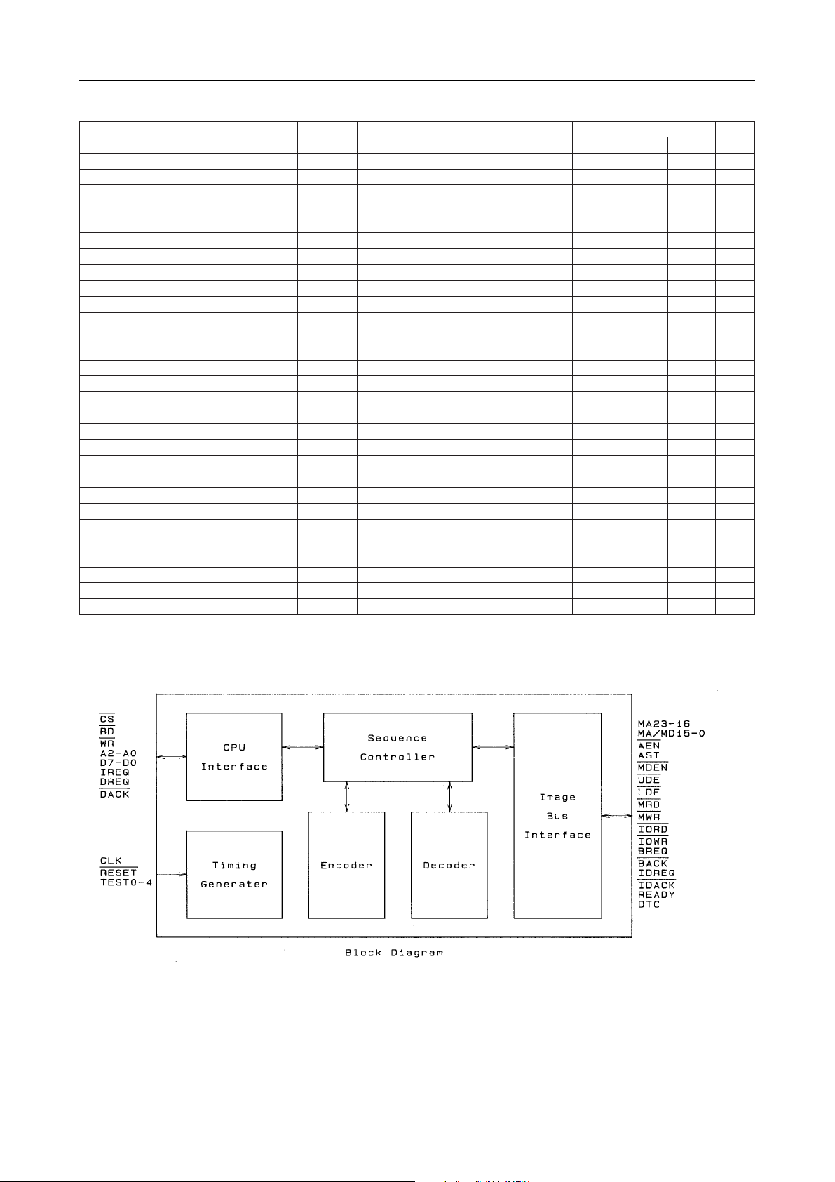
Block Diagram
No.4605–3/10
Page 4

LC8213
• CPU interface
This is an interface circuit with the general purpose 8-bit CPU. The operation mode can be set, etc., by accessing the
interface register and parameter register.
• Sequence controller
Each block is controlled by the coded and decoded process algorithm.
• Coding section
The change points of the pixels are detected and judged, and a code in each mode is generated. The coded data is
transferred to the data bus via the FIFO (EFIFO) for 8-bit × 4-word coding.
• Decoding section
The coded data in each mode is judged and the reproduced pixel data is generated. The coded data is transferred to the
data bus via the FIFO (DFIFO) for decoding.
• Image memory interface
Reading and writing of the image memory and control of the DMA transfer on the image memory bus is performed.
Pin Assignment
I : Input pin
O : Output pin
B : Bidirectional pin
P : Power pin
NC : Not connected
.oNemanniPepyT
1SCI
2DRI
3RWI
42AI
51AI
60AI
7VDDP
8CN
97DB
016DB
115DB
214DB
31VSSP
413DB
512DB
611DB
710DB
81CN
91VDDP
02QERIO
12QERDO
22KCADI
32CN
42CN
52CN
62CN
72TESERI
82KLCI
92VSSP
034TSETI
.oNemanniPepyT
13VDDP
233TSETI
332TSETI
431TSETI
530TSETI
63CN
73QERBO
83KCABI
93QERDII
04KCADIO
14NEAO
24TSAO
34NEDMO
44DRMO
54RWMO
64DROIO
74RWOIO
84EDLO
94EDUO
05YDAERI
15CTDO
25VSSP
35VDDP
4532AMO
5522AMO
6512AMO
7502AMO
8591AMO
9581AMO
0671AMO
.oNemanniPepyT
1661AMO
2651DM/AMO
36VSSP
4641DM/AMB
5631DM/AMB
6621DM/AMB
7611DM/AMB
8601DM/AMB
969DM/AMB
078DM/AMB
177DM/AMB
27VSSP
37VDDP
476DM/AMB
575DM/AMB
674DM/AMB
773DM/AMB
872DM/AMB
971DM/AMB
080DM/AMB
No.4605–4/10
Page 5

Pin Descriptions
CPU Interface
emanniP.oNniPO/IsnoitpircseD
SC1I .)evitcawol(3128CLehtsseccaotUPCehtroftcelespihC
DR2I .retsiger3128CLehttuodaerotsiUPCehtnehw"L"otteS.daeR
RW3I .retsiger3128CLehttuoetirwotsiUPCehtnehw"L"otteS.etirW
2A
1A
0A
7D
6D
5D
4D
3D
2D
1D
0D
QERI02O
QERD12O
KCAD22I
4
5
6
9
01
11
21
41
51
61
71
I.3128CLsesseccaUPCehtnehwroftupnisserddA
O/I
setats3
LC8213
subatadtib-8lanoitceridiB
ehtdnifnacUPCeht)retsigertseuqertpurretni(RTNIehttuognidaeryB.UPCehtroflangistseuqertpurretnI
.RTNIsdaerUPCehtnehw"L"ottessiQERI.noitpurretniehtfoesuac
.sesacgniwollofehtni"H"otteseblliwsihT.rellortnocAMDlanretxeehtroflangistseuqerAMD
.sessecorpgnidocehtgnirudOFIFEehtnistsixeataD*
.sessecorpgnidocedgnirudOFIFDehtnistsixeecapsytpmenA*
.subUPCdnasubyromemegamiehtneewtebrefsnartatadgnirudetirw/daernacFUBDehT*
,gnidocedrognidocgnirud"L"ottessiKCADfI.rellortnocAMDlanretxeehtmorflangisegdelwonkcaAMD
neewtebrefsnartatadgnirud"L"ottessiKCADfidesseccaeblliwFUBD.desseccaeblliwOFIFDdnaOFIFE
.subUPCdnasubyromemegamieht
Image Memory Interface
emanniP.oNniPO/IsnoitpircseD
32AM
22AM
12AM
02AM
91AM
81AM
71AM
61AM
51DM/AM
41DM/AM
31DM/AM
21DM/AM
11DM/AM
01DM/AM
9DM/AM
8DM/AM
7DM/AM
6DM/AM
5DM/AM
4DM/AM
3DM/AM
2DM/AM
1DM/AM
0DM/AM
NEA14O
TSA24O .0DM/AMot51DM/AMottuptuogniebsisserddanatahtsetacidnilangissihT
NEDM34O .sesubatadsa0DM/AMot51DM/AMgnisusi3128CLehttahtsetacidnilangissihT
EDU94
EDL84
DRM44
RWM54
DROI64
RWOI74
QERB73O .subyromemegamiehtmorfsthgiregasutseuqerot3128CLehtrofdesusilangissihT
KCAB83I .subyromemegamiehtesuot3128CLehtgniwollalangistupnI
QERDI93I .3128CLehtmorfAMDtseuqerotecivedO/IehtrofdesulangistupnI
KCADI04O .3128CLmorflangisegdelwonkcaAMD
YDAER05I .ecivedO/Inaroyromemegamideepswolgnisunehwlangisetirw/daerehtyaledotdesusilangissihT
CTD15O .detelpmocneebsahrefsnartAMDehttahtsetacidnilangissihT
45
55
65
75
85
95
06
16
26
46
56
66
76
86
96
07
17
47
57
67
77
87
97
08
O
setats3
O/I
setats3
O
setats3
O
setats3
O
setats3
O
setats3
O
setats3
O
setats3
.yromemegamiehtfosserddatib-8redro-hgiH
.yromemegamiehtrofsubatadtib-61dnasserddatib-61redro-woL
.tuptuoZiHaeblliwEDLdnaEDU,RWOI,DROI
.desugnieberasubatadehtfostibredro-hgihehttahtsetacidnilangissihT
.desugnieberasubatadehtfostibredro-wolehttahtsetacidnilangissihT
.yromemegamiehtfotuodaergniebsiatadnehw"L"ottessisihT
.yromemegamiehtotninettirwgniebsiatadnehw"L"ottessisihT
.ecivedO/Iehtfotuodaergniebsiatadnehw"L"ottessisihT
.ecivedO/Iehtotninettirwgniebsiatadnehw"L"ottessisihT
,RWM,DRM,DM/AM,"H"=NEAfI.yromemegamiehtotretsamsubehtsi3128CLehtnehw"L"ottessisihT
No.4605–5/10
Page 6

LC8213
Others
emanniP.oNniPO/IsnoitpircseD
KLC82I )zHM02.xaM(kcolclanretxE
TESER72IteseR
0TSET
1TSET
2TSET
3TSET
4TSET
V
DD
V
SS
Explanation of Function
• Coding method
The coding method follows the CCITT T.4, T.6 MH, MR and MMR coding methods that are the standard for the G3 and
G4 facsimiles.
• Processing mode
A maximum of 64k lines for processing can be set, and processing per block is possible. Processing per line is also
possible. The coding and decoding FIFOs are built-in, and coding and decoding can be performed alternately for se v eral
lines at a time.
When coding, the LC8213 reads the image data in order from the start address of the image memory set in the register.
This data is coded and written into the coding FIFO. When the set number of lines have been processed, the CPU is
interrupted.
When decoding, the LC8213 reads the coded data from the decoding FIFO, reproduces the image data, and writes it into
the image memory. When the set number of lines have been processed or a decoding error occurs, the CPU is interrupted.
• Line skip mode
This mode allows the coded amount of blank lines to be decreased to half of the minimum transmission bits. The line
skip bit (blank line judgement bit) is added to the end of the EOL code, and a fill bit is added to the blank line so that the
coded amount is half of the minimum transmission bits. For lines that are not completely blank, the normal codes are
transmitted after the line skip bit.
• CPU interface
This interface has an 8-bit data bus, and various operation modes can be set by accessing the interface register. As
interface terminals for the external DMA controller are built-in, DMA transfer between the LC8213 and the CPU bus
memory is possible.
• Image memory interface
The image memory address space has 16M bytes.
The data bus size can be selected from 8-bit or 16-bit.
• DMA transfer function
DMA transfer is performed between the image memory and I/O device with the internal DMA controller. A maximum
of 64k lines can be set for transferring.
• Data transfer function
Data transfer can be performed without coding/decoding between the CPU bus and image memory bus.
• Pad bit processing
Pad bit processing can be selected. Pad bit processing is a function that outputs a “0” after 1 line of coded data so that it
is an 8-bit unit.
• Parameter settings
The following parameters can be set to the listed values.
· No. of processing bits per line (byte unit) 1 to 8k bytes
· Document width (byte unit) 1 to 8k bytes
· No. of processing lines 1 to 64k
· Minimum transmission bits per line 0 to 64k
· K parameters during MR coding 0 to 64k
· No. of processing lines for DMA transfer 1 to 64k
· No. of EOL that structure RTC code 0 to 255
The document width and no. of processing bits per line can be set separately, so a part of the document can be cut
and coded or decoded.
53
43
33
23
03
,13,9,7
37,35
27,36
IgnitsetroF
,25,92,31
DNG
."L"otdexifyllamronsisihT
)V5+(ylppusrewoP
No.4605–6/10
Page 7

LC8213
CPU Read Timing
CPU Write Timing
DMA Controller Read Timing
DMA Controller Write Timing
No.4605–7/10
Page 8

LC8213
Image Memory Access
No.4605–8/10
Page 9

LC8213
DMA Transfer
Clock Reset Timing
No.4605–9/10
Page 10

LC8213
Specifications of any and all SANYO products described or contained herein stipulate the performance,
characteristics, and functions of the described products in the independent state, and are not guarantees
of the performance, characteristics, and functions of the described products as mounted in the customer's
products or equipment. To verify symptoms and states that cannot be evaluated in an independent device,
the customer should always evaluate and test devices mounted in the customer's products or equipment.
SANYO Electric Co., Ltd. strives to supply high-quality high-reliability products. However, any and all
semiconductor products fail with some probability. It is possible that these probabilistic failures could
give rise to accidents or events that could endanger human lives, that could give rise to smoke or fire,
or that could cause damage to other property. When designing equipment, adopt safety measures so
that these kinds of accidents or events cannot occur. Such measures include but are not limited to protective
circuits and error prevention circuits for safe design, redundant design, and structural design.
In the event that any or all SANYO products(including technical data,services) described or
contained herein are controlled under any of applicable local export control laws and regulations,
such products must not be exported without obtaining the export license from the authorities
concerned in accordance with the above law.
No part of this publication may be reproduced or transmitted in any form or by any means, electronic or
mechanical, including photocopying and recording, or any information storage or retrieval system,
or otherwise, without the prior written permission of SANYO Electric Co. , Ltd.
Any and all information described or contained herein are subject to change without notice due to
product/technology improvement, etc. When designing equipment, refer to the "Delivery Specification"
for the SANYO product that you intend to use.
Information (including circuit diagrams and circuit parameters) herein is for example only ; it is not
guaranteed for volume production. SANYO believes information herein is accurate and reliable, but
no guarantees are made or implied regarding its use or any infringements of intellectual property rights
or other rights of third parties.
This catalog provides information as of August, 2001. Specifications and information herein are subject to
change without notice.
PS No.4605–10/10
 Loading...