

Page 1
Ordering number: EN 4101B
CMOS LSI
LC7986C
LCD Controller/Driver
Overview
The LC7986C is a low-power CMOS IC that incorporates
dot-matrix character generator, display controller and
driver functions in a single device, and realizes ideal for
use in portable equipment containing LCD displays.
Also, the CMOS process realizes easy expansion to control displays of up to 80 characters by adding LC7930N or
LC7931D display drivers.
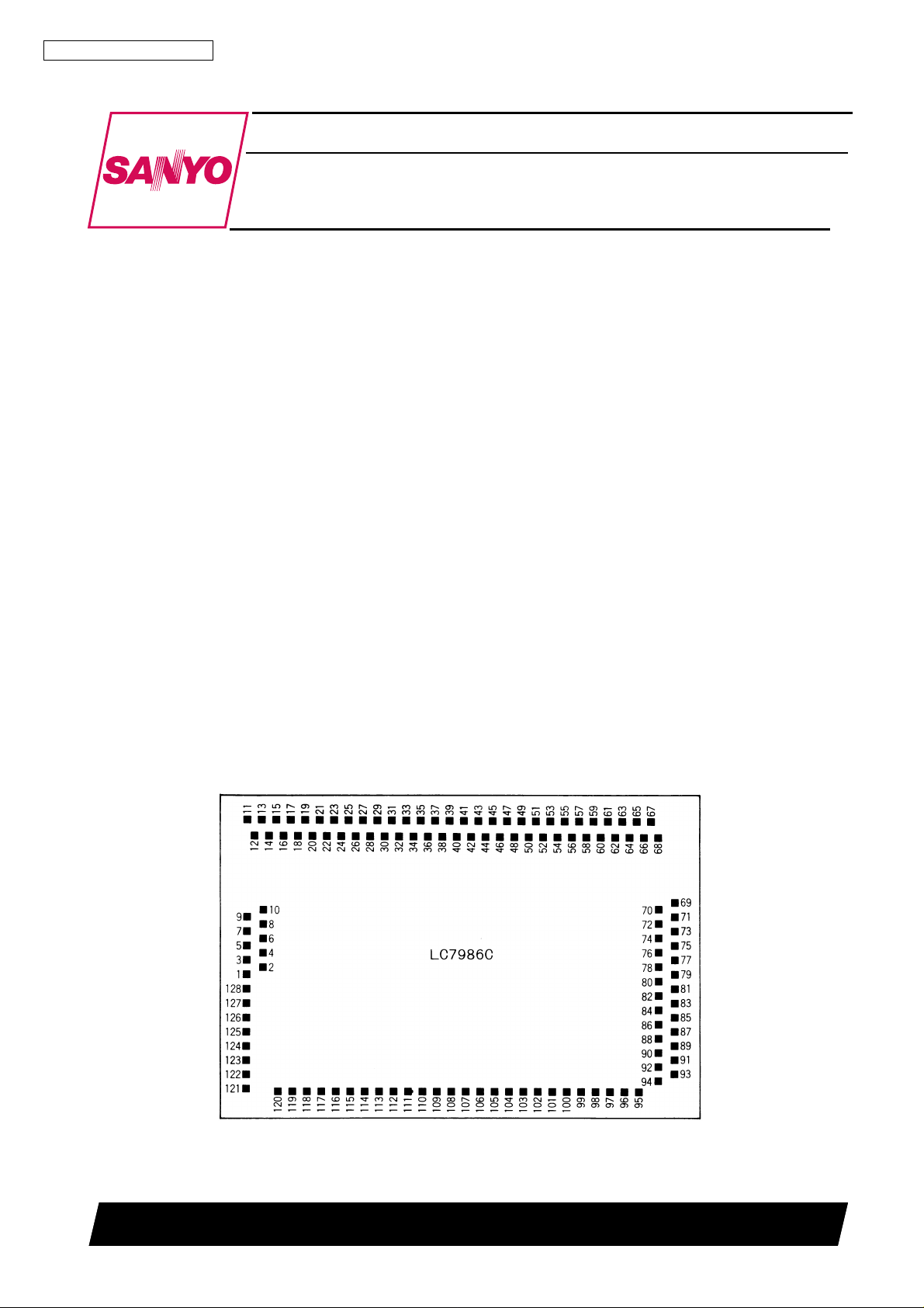
Pad Layout
Chip size: 5.69 × 3.45mm
2
Features
• Controller and driver for dot-matrix LCD displays
• 5 × 7-pixel and 5 × 10-pixel character fonts
• 160, 5 × 7-pixel characters and 32, 5 × 10-pixel characters in character generator ROM
• Eight, 5 × 7-pixel characters or four, 5 × 10-pixel characters in character generator RAM
• 80-character display data RAM
• Built-in drivers for 1-line × 16-character and 2-line ×
16-character displays
• Easy expansion to 1-line × 80-character or 2-line × 40character displays by adding LC7930Ns or LC7931Ds
• 4-bit or 8-bit microcontroller interface
• 11 microcontroller instructions
• Built-in reset circuit
• Built-in oscillator
• 5V supply
• 128-pad dice
SANYO Electric Co., Ltd. Semiconductor Business Headquarters
TOKYO OFFICE Tokyo Bldg., 1-10, 1 Chome, Ueno, Taito-ku, TOKYO, 110 JAPAN
70197HA (ID) / D082JN No. 4101—1/32
Page 2
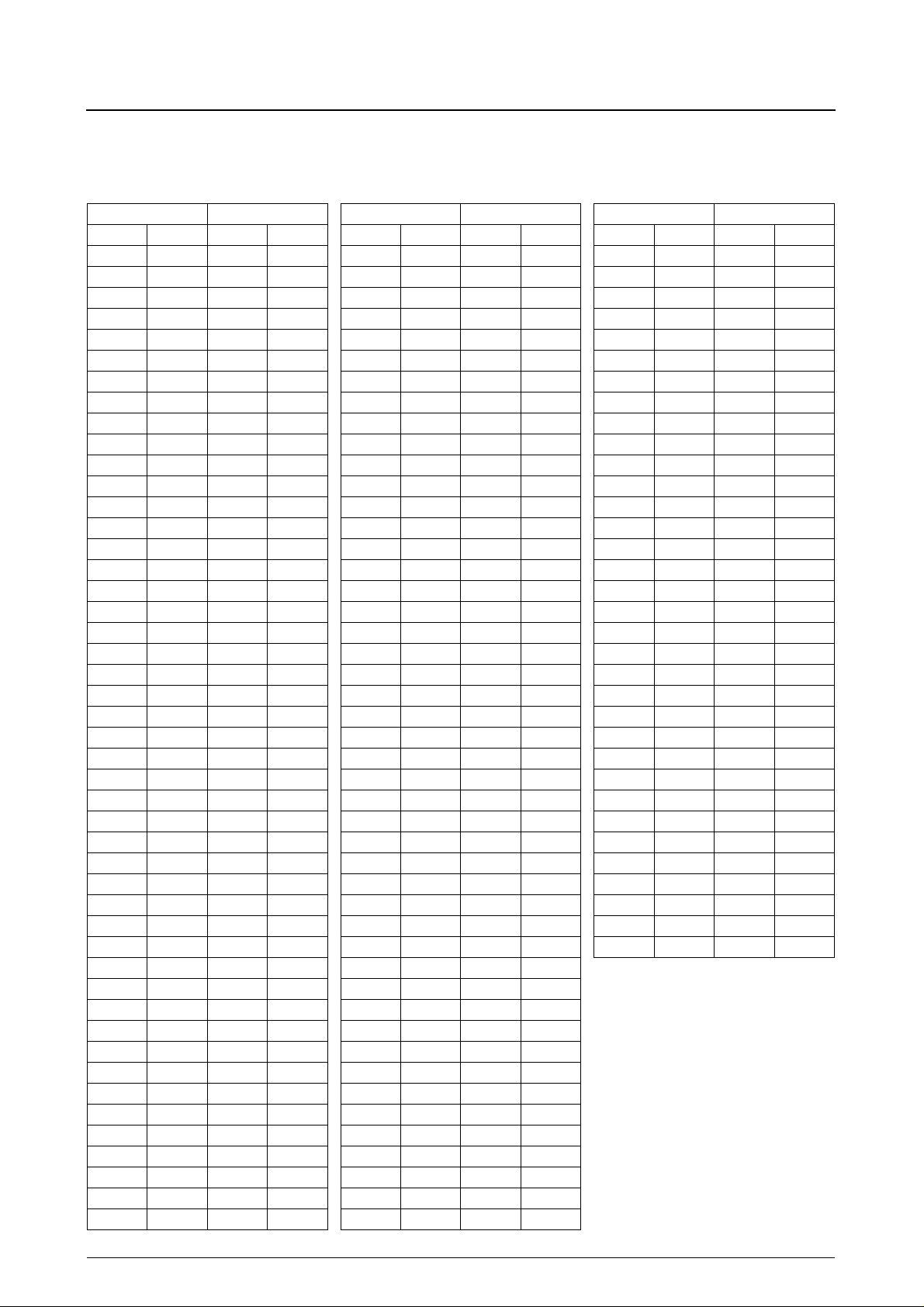
−
Pad Coordinates
The coordinate origin is in the center of the chip.
LC7986C
−
Pad Coordinates
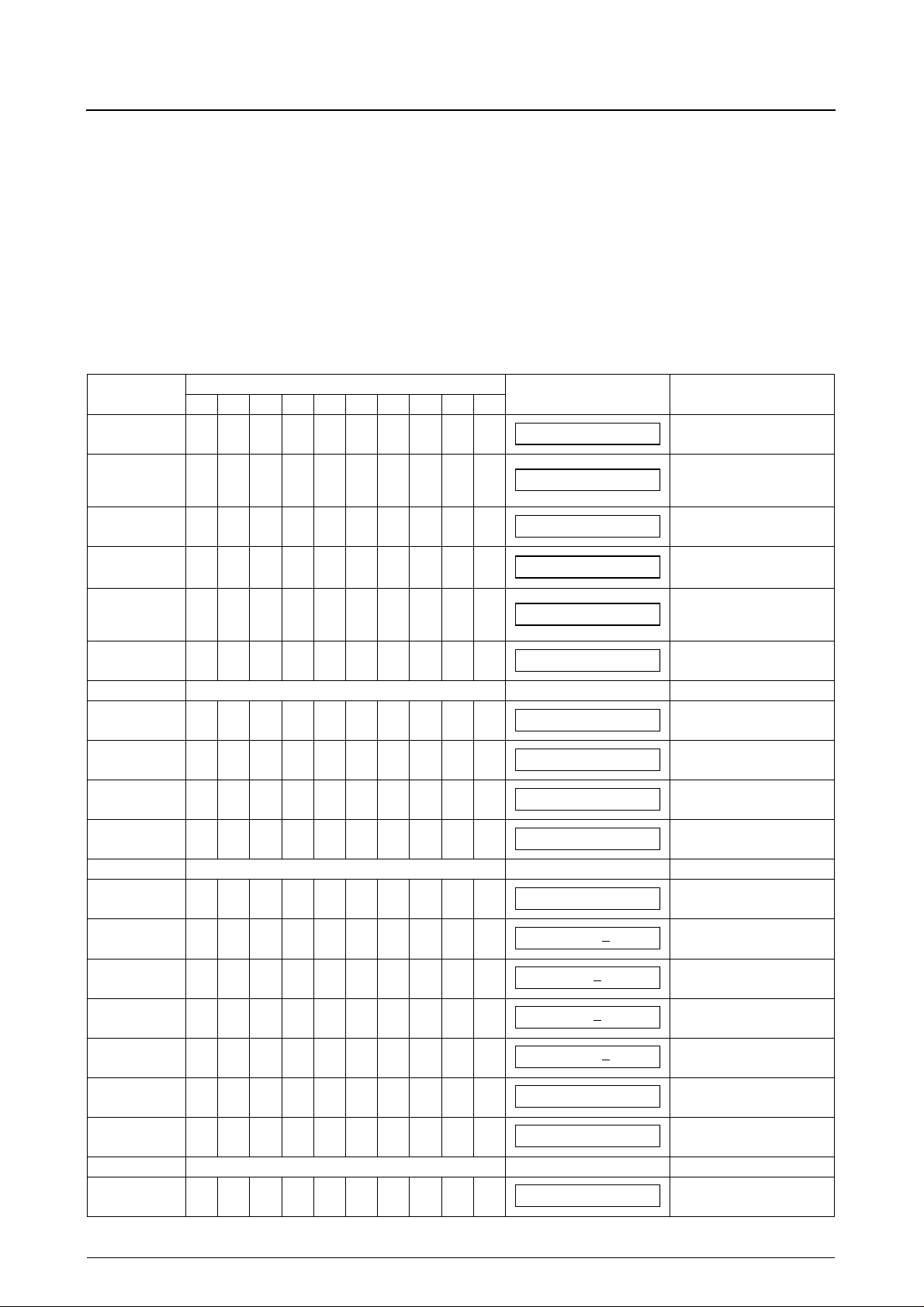
Number Name X Y
1 OS1 2660.0 76.9
2 OS2 2500.0 − 13.1
3 OS3 2660.0 − 103.1
4 OS4 2500.0 − 193.1
5 OS5 2660.0 − 283.1
6 OS6 2500.0 − 373.1
7 OS7 2660.0 − 463.1
8 OS8 2500.0 − 553.1
9 OS9 2660.0 − 643.1
10 OS10 2500.0 − 733.1
11 OS11 2581.4
12 OS12 2491.4 − 1380.0
13 OS13 2401.4 − 1540.0
14 OS14 2311.4 − 1380.0
15 OS15 2221.4 − 1540.0
16 OS16 2131.4 − 1380.0
17 OS17 2041.4 − 1540.0
18 OS18 1951.4 − 1380.0
19 OS19 1861.4 − 1540.0
20 OS20 1771.4 − 1380.0
21 OS21 1681.4 − 1540.0
22 OS22 1591.4 − 1380.0
23 OS23 1501.4 − 1540.0
24 OS24 1411.4 − 1380.0
25 OS25 1321.4 − 1540.0
26 OS26 1231.4 − 1380.0
27 OS27 1141.4 − 1540.0
28 OS28 1051.4 − 1380.0
29 OS29 961.4 − 1540.0
30 OS30 871.4 − 1380.0
31 OS31 781.4 − 1540.0
32 OS32 691.4 − 1380.0
33 OS33 601.4 − 1540.0
34 OS34 511.4 − 1380.0
35 OS35 421.4 − 1540.0
36 OS36 331.4 − 1380.0
37 OS37 241.4 − 1540.0
38 OS38 151.4 − 1380.0
39 OS39 61.4 − 1540.0
40 OS40 − 28.6 − 1380.0
41 OS41 − 118.6 − 1540.0
42 OS42 − 208.6 − 1380.0
43 OS43 − 298.6 − 1540.0
44 OS44 − 388.6 − 1380.0
45 OS45 − 478.6 − 1540.0
46 OS46 − 568.6 − 1380.0
47 OS47 − 658.6 − 1540.0
1540.0
Pad Coordinates
Number Name X Y
48 OS48 − 748.6 − 1380.0
49 OS49 − 838.6 − 1540.0
50 OS50 − 928.6 − 1380.0
51 OS51 − 1018.6 − 1540.0
52 OS52 − 1108.6 − 1380.0
53 OS53 − 1198.6 − 1540.0
54 OS54 − 1288.6 − 1380.0
55 OS55 − 1378.6 − 1540.0
56 OS56 − 1468.6 − 1380.0
57 OS57 − 1558.6 − 1540.0
58 OS58 − 1648.6 − 1380.0
59 OS59
60 OS60 − 1828.6 − 1380.0
61 OS61 − 1918.6 − 1540.0
62 OS62 − 2008.6 − 1380.0
63 OS63 − 2098.6 − 1540.0
64 OS64 − 2188.6 − 1380.0
65 OS65 − 2278.6 − 1540.0
66 OS66 − 2368.6 − 1380.0
67 OS67 − 2458.6 − 1540.0
68 OS68 − 2548.6 − 1380.0
69 OS69 − 2660.0 − 733.1
70 OS70 − 2500.0 − 643.1
71 OS71 − 2660.0 − 553.1
72 OS72 − 2500.0 − 463.1
73 OS73 − 2660.0 − 373.1
74 OS74 − 2500.0 − 283.1
75 OS75 − 2660.0 − 193.1
76 OS76 − 2500.0 − 103.1
77 OS77 − 2660.0 − 13.1
78 OS78 − 2500.0 76.9
79 OS79 − 2660.0 166.9
80 OS80 − 2500.0 256.9
81 OC16 − 2660.0 370.0
82 OC15 − 2500.0 460.0
83 OC14
84 OC13−2500.0 640.0
85 OC12−2660.0 730.0
86 OC11−2500.0 820.0
87 OC10−2660.0 910.0
88 OC9
89 OC8
90 OC7
91 OC6
92 OC5
93 OC4
94 OC3
1738.6 − 1540.0
−
2660.0 550.0
−
2500.0 1000.0
−
2660.0 1090.0
−
2500.0 1180.0
−
2660.0 1270.0
−
2500.0 1360.0
−
2660.0 1450.0
−
2500.0 1540.0
Pad Coordinates
Number Name X Y
95 OC2
96 OC1
97 V1’
98 V1
99 V2’
100 V2
101 V3’
102 V3
103 V4’
104 V4
105 V5’
106 V5
107 V
108 V
109 OSCO 218.9 1540.0
110 OSCR 378.9 1540.0
111 OSCI 538.9 1540.0
112 CP 698.9 1540.0
113 LOAD 858.9 1540.0
114 M 1018.9 1540.0
115 D 1178.9 1540.0
116 SHL 1338.9 1540.0
117 A/B 1498.9 1540.0
118 E 1658.9 1540.0
119 R/W 1818.9 1540.0
120 RS 1978.9 1540.0
121 DB7 2660.0 1540.0
122 DB6 2660.0 1360.0
123 DB5 2660.0 1180.0
124 DB4 2660.0 1000.0
125 DB3 2660.0 820.0
126 DB2 2660.0 640.0
127 DB1 2660.0 460.0
128 DB0 2660.0 280.0
SS
DD
−
2217.5 1540.0
−
2037.5 1540.0
−
1701.1 1540.0
−
1541.1 1540.0
−
1381.1 1540.0
−
1221.1 1540.0
−
1061.1 1540.0
−
901.1 1540.0
−
741.1 1540.0
−
581.1 1540.0
−
421.1 1540.0
−
261.1 1540.0
−
101.1 1540.0
58.9 1540.0
No. 4101—2/32
Page 3
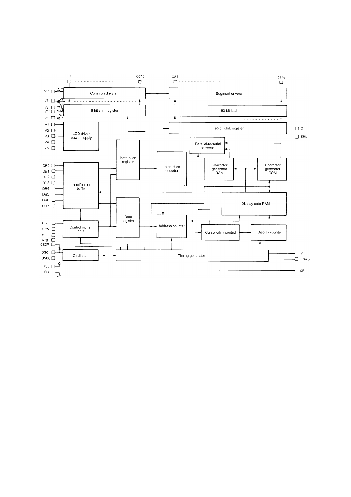
Block Diagram
LC7986C
No. 4101—3/32
Page 4
LC7986C
Specifications
The following characteristics apply to the ceramic-packaged device.
Absolute Maximum Ratings at Ta = 25 ± 2°C, V
SS
= 0V
Parameter Symbol Ratings Unit
Supply voltage range V
LCD drive supply voltage range
*1
Input voltage range V
DD max
V1 to V
I
5
VDD − 13.5 to VDD + 0.3 V
−
0.3 to VDD + 0.3 V
Storage temperature range Tstg
Note: *1. VDD must obey the relationship: VDD ≥ V1 ≥ V2 ≥ V3 ≥ V4 ≥ V5
Allowable Operating Ranges at Ta = −20 to +75°C
Parameter Symbol Conditions
Supply voltage V
LCD driver reference voltages
*1
High-level input voltage
Low-level input voltage
DD
V
D5
V
D1
V
IH1
V
IH2
V
IL1
V
IL2
VD5 = VDD − V
VD1 = VDD − V
5
1
RS, R/W, E, DB0 to DB7 2.2 – V
OSCI, SHL, A/B VDD − 1.0 – V
RS, R/W, E, DB0 to DB7 – – 0.6 V
OSCI, SHL, A/B – – 1.0 V
min typ max
4.5 – 5.5 V
1.5 – 6.0 V
– – 0.25V
Note: *1. These voltages guarantee correct operation of the LSI. They do not guarantee correct operation of the LCD panel. V
Ratings
−
0.3 to +7.0 V
−
55 to +125
D5
DD
DD
must also be observed.
LCD
°
C
Unit
V
V
V
Electrical Characteristics at Ta = −20 to +75°C, V
Parameter Symbol Conditions
IOH = −0.205mA,
input/output pins
IOH = −0.04mA,
output pins
IOL = 1.2mA,
input/output pins
IOL = 0.04mA,
output pins
Id = 0.05mA – – 2.9 V
Id = 0.05mA – – 3.8 V
VI = VSS to V
VDD = 5V,
RS, R/W, DB0 to DB7
High-level output voltage
Low-level output voltage
OC1 to OC16 driver voltage drop
OS1 to OS40 driver voltage drop
*1
*2
Input/output leakage current I
Pull-up current I
V
V
V
V
V
V
OH1
OH2
OL1
OL2
COM
SEG
L
P
= 0V, VDD = 5V ± 10%, unless otherwise noted
SS
Ratings
min typ max
2.4––V
0.9V
DD
––V
– – 0.4 V
– – 0.1V
DD
––1
50 125 250
DD
External feedback Rf
Supply current I
DD
oscillator, VDD = 5V, f
320kHz, no output load
OSC
=
– 0.5 1.0
Internal feedback Rf oscillator – 0.5 1.0
External clock operating frequency f
CP
125 – 410 kHz
External clock duty cycle DUTY 45 50 55 %
External clock rise time t
External clock fall time t
r
f
– – 0.2
– – 0.2
Unit
V
µ
A
µ
A
mA
µ
s
µ
s
No. 4101—4/32
Page 5

LC7986C
Parameter Symbol Conditions
Internal oscillator operating frequency f
OSC
min typ max
Using Rf = 56kΩ ± 3% 220 320 420
Using built-in Vf – 320 –
Ratings
RC oscillator built-in resistance Vf OSCO to OSCR – 56 – k
V
LCD display voltage
Voltage divider step resistance V
Note: *1. V
Note: *2. V
is the voltage from VDD, V1, V4 and V5 to the LCD common drive pins OC1 to OC16.
COM
is the voltage from VDD, V2, V3 and V5 to the LCD segment drive pins OS1 to OS80.
SEG
LCD1
V
LCD2
R
Switching Characteristics at Ta = −20 to +75°C, V
Parameter Symbol Conditions
E cycle time t
E high-level pulsewidth t
E rise time t
E fall time t
RS and R/W to E setup time t
E to RS and R/W address hold time t
DB0 to DB7 to E data setup time t
Write cycle E to DB0 to DB7 data hold
time
Read cycle E to data valid delay time t
Read cycle E to DB0 to DB7 data hold
time
CP low-level pulsewidth t
CP high-level pulsewidth t
CP to LOAD setup time t
D to CP data setup time t
CP to D data hold time t
LOAD to M delay time t
ECYC
EW
ER
EF
SU
AH
DSU
t
DHW
DD
t
DHR
WL
WH
CSU
DSU
DH
DM
VDD − V5 (1/5 bias) 4.6 – 6 V
VDD − V5 (1/4 bias) 3.0 – 6 V
Between V(n) and V(n+1) – 2.2 – k
= 0V, VDD = 5V ± 10%
SS
Ratings
min typ max
1000 – – ns
450 – – ns
– – 25 ns
– – 25 ns
140 – – ns
10––ns
195 – – ns
10––ns
See measurement circuit. – – 320 ns
20––ns
800 – – ns
800 – – ns
500 – – ns
300 – – ns
300 – – ns
−
1000 – 1000 ns
Unit
kHz
Ω
Ω
Unit
Reset characteristics at Ta = −20 to +75°C
Parameter Symbol Conditions
VDD rise time t
VDD off time t
DDR
DDOFF
Ratings
min typ max
1 – 100
Unit
µ
s
1––ms
No. 4101—5/32
Page 6
LC7986C
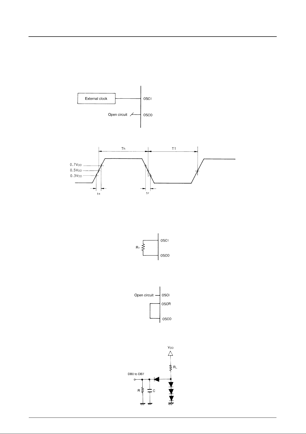
Clock Generator
The internal oscillator that generates the clock for the internal circuit requires an external feedback resistor, connection of
the internal feedback resistor or an external clock input as shown in the following sections.
External clock
The input duty cycle should be between 45 and 55% as shown in the following figure.
External feedback resistor
Internal feedback resistor
Measurement Circuit
T
h
Note.
Note. The resistor should be mounted as close as possible to OSCI and OSCO.
Duty
-----------------
ThT1+
×=
100%
Note. R
= 2.4kΩ, C = 130pF, R = 11k
L
Ω
No. 4101—6/32
Page 7
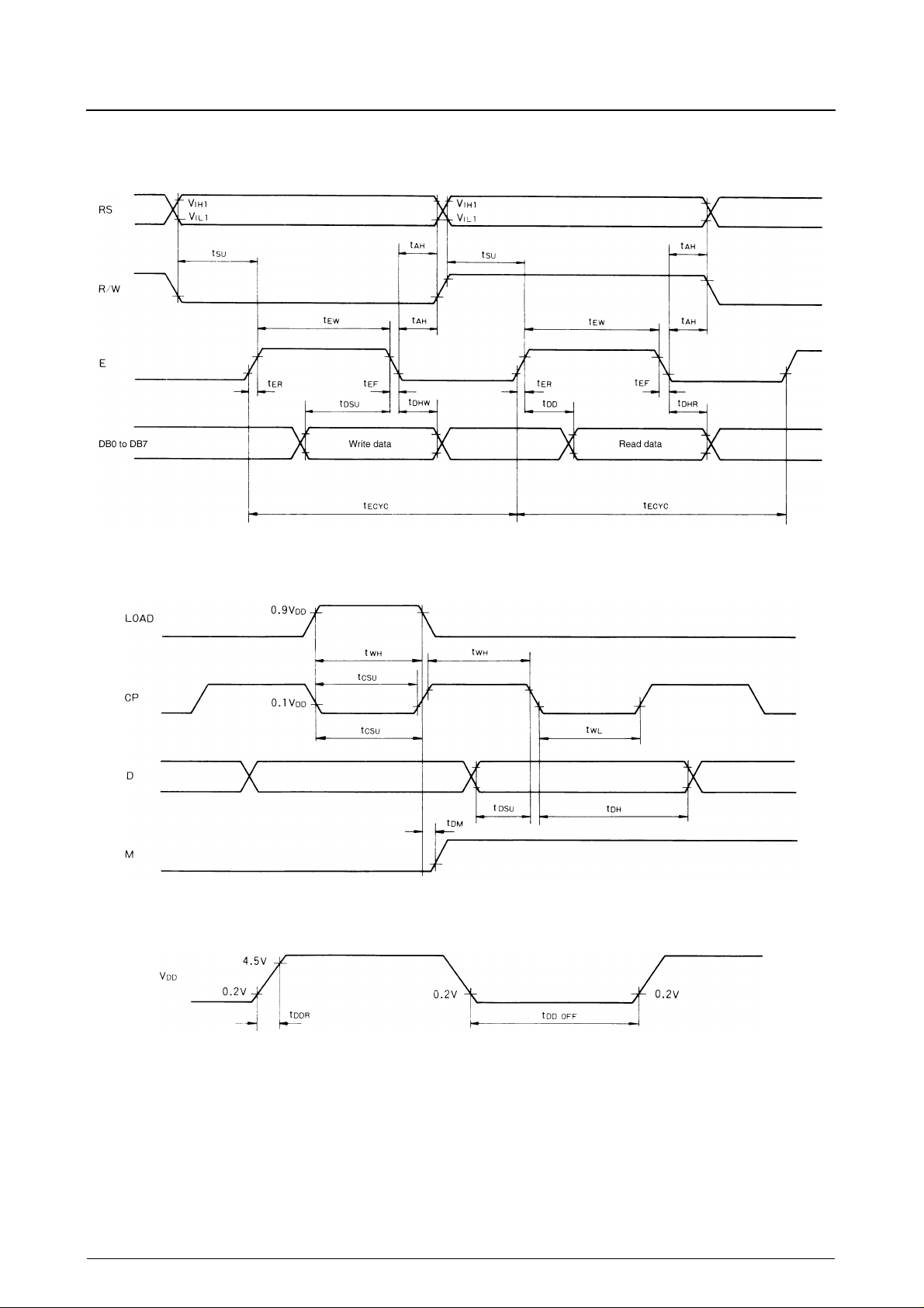
Read/write cycle timing
LC7986C
LC7930N interface timing
Power Supply
No. 4101—7/32
Page 8
LC7986C
Pin Description
Name Num I/O Connect to Functions
RS 1 I MPU Data register or instruction register select input. Data register when "1" and instruction register when "0".
R/W 1 I MPU Read or write select input. Read when "1" and write when "0".
E 1 I MPU Execution start input
DB7 to DB4 4 I/O MPU
DB3 to DB0 4 I/O MPU
LOAD 1 O LC7930N D serial data shift latch output
CP 1 O LC7930N D serial data shift clock output
M 1 O LC7930N Display expansion drive signal inversion control signal output
D 1 O LC7930N Display expansion serial data output. Nonselected when "0" and selected when "1".
OC1 to OC16 16 O LCD
OS1 to OS80 80 O LCD LCD segment driver outputs
V1 to V5 5 source LCD driver reference voltage inputs
, GND 2 source VDD : +5V, GND : 0V
V
DD
OSCI 2 Oscillator feedback resistor connection and external clock input
OSCO 2 Oscillator external feedback resistor connection
OSCR 1 OSCO Internal feedback resistor connection. Connect to OSCI or leave open.
SHL 1 I
A/B 1 I M output signal type select input. A-type when "1" and B-type when "0".
V1’ to V5’ 5 I VDD to V4 LCD drive voltage internal voltage divider outputs. Leave open if the the voltage divider is not used.
4-bit microcontroller interface data bus and 8-bit microcontroller interface high-order four bits data bus
connections. DB7 can also be used as busy flag.
8-bit microcontroller interface low-order four bits data bus connections. No connection when 4-bit interface
size is selected.
LCD common driver outputs. OC9 to OC16 and OC12 to OC16 are unselected in 1/8 duty and 1/11 duty
respectively.
Segment output shift direction select input. Shift right (OS1 to OS80) when"1", and shift left (OS80 to OS1)
when "0".
No. 4101—8/32
Page 9

Functional Description
Registers
LC7986C
The LC7986C has two 8-bit registers—instruction register
(IR) and data register (DR)—that are selected as shown in
the following table.
RS R/W Operation
0 0 IR write, instruction execution
0 1 Busy flag (DB7) and address counter (DB0 to DB6) output
1 0 DR write, internal DR to DD RAM or CG RAM data transfer
1 1 DR read, internal DD RAM or CG RAM to DR data transfer
The instruction register is write-only. It contains instruction codes or DD RAM and CG RAM addresses written
by the microcontroller.
Busy Flag
When busy flag is 1, the previous instruction is executing,
and when 0, the instruction has completed. The next
instruction cannot be received until BF is 0. The microcontroller should, therefore, confirm that BF is 0 before writing the next instruction.
Display Data RAM (DD RAM)
The data register holds data read from or written to either
DD RAM or CG RAM. Data written to the data register by
the microcontroller is automatically transferred to the current DD RAM or CG RAM address. Data read from
DD RAM or CG RAM is buffered in the data register.
When the microcontroller writes a DD RAM or CG RAM
address to the instruction register, the data at that address
is copied into the data register. The microcontroller then
reads the data in the data register to complete the transfer.
Once that data is read, the data from the next DD RAM or
CG RAM address is copied into the data register in preparation for the next data read.
Address Counter
The address counter is used for both the DD RAM and the
CG RAM. The address output on DB0 to DB7 is the
counter value before the currently executing instruction
began.
The display data RAM stores 80, 8-bit character codes, and the LC7986C can display a maximum of 80 characters. The
address counter contains the location for the next display memory read or write operation as shown in the following figure.
Display data addresses are in hexadecimal. For example, the address counter contents for location 4E are shown in the
following figure.
To prevent undesirable effects such as display flicker during DD RAM accesses, the internal memory and the microprocessor interface have separate timing signals.
Single-line display mode (N = 0)
The DD RAM addresses and their corresponding display positions for an 80-character display are shown in the following
figure.
No. 4101—9/32
Page 10
LC7986C
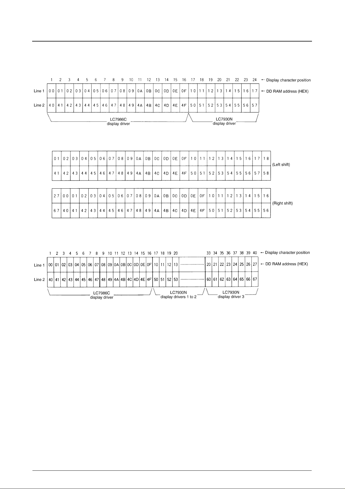
A single LC7986C, however, can drive 16 characters. The display positions and DD RAM addresses for an unshifted 16character display are shown in the following figure.
The DD RAM addresses following left and right display shifts are shown in the following figure. Note that the displayed
characters wrap around from addresses 4FH to 00H.
An LC7986C and a single LC7930N can drive a 16-character display. The display positions and DD RAM addresses for
an unshifted display are shown in the following figure.
The DD RAM addresses following left and right display shifts are shown in the following figure.
The number of displayed characters can be increased by adding more LC7930Ns. An LC7986C and eight LC7930Ns can
drive an 80-character display as shown in the following figure.
No. 4101—10/32
Page 11

LC7986C
Shift direction
The segment driver shift register is bidirectional. When SHL is HIGH, the shift direction is right-to-left, and characters
are displayed normally. When SHL is LOW, the shift direction is left-to-right, and the display position, DD RAM
addresses and character bitmaps are all reversed as shown in the following figure.
Two-line display mode (N = 1)
The DD RAM addresses and their corresponding display positions for a 2-line × 40-character display are shown in the
following figure. Note that the address counter automatically increments from 27H to 40H.
A single LC7986C, however, can drive 16 characters per line. The display positions and DD RAM addresses for an
unshifted, 2-line × 16-character display are shown in the following figure.
The display positions following a left or right display shift are shown in the follo wing figure. Note that the display shift is
simultaneous for both lines, regardless of which line the cursor is in.
No. 4101—11/32
Page 12
LC7986C
An LC7986C and a single LC7930N can drive a 2-line × 24-character display. The display positions and DD RAM
addresses for an unshifted, 2-line × 24-character display are shown in the following figure.
The DD RAM addresses following left and right display shifts are shown in the following figure.
The number of displayed characters can be increased by adding more LC7930Ns. An LC7986C and three LC7930Ns can
drive a 2-line × 40-character display as shown in the following figure.
Character Generator ROM (CG ROM)
The character generator ROM contains 160, 5 × 7-pixel bitmaps and 32, 5 × 10-pixel bitmaps as shown in the following
figure. The characters are selected by their 8-bit character code.
Character Generator RAM (CG RAM)
The character generator RAM stores user-defined bitmaps for either eight, 5 × 7-pixel characters or four, 5 × 10-pixel
characters. To display character patterns stored in CG RAM, write the character codes, shown in the leftmost column of
the following figure, on DD RAM.
No. 4101—12/32
Page 13
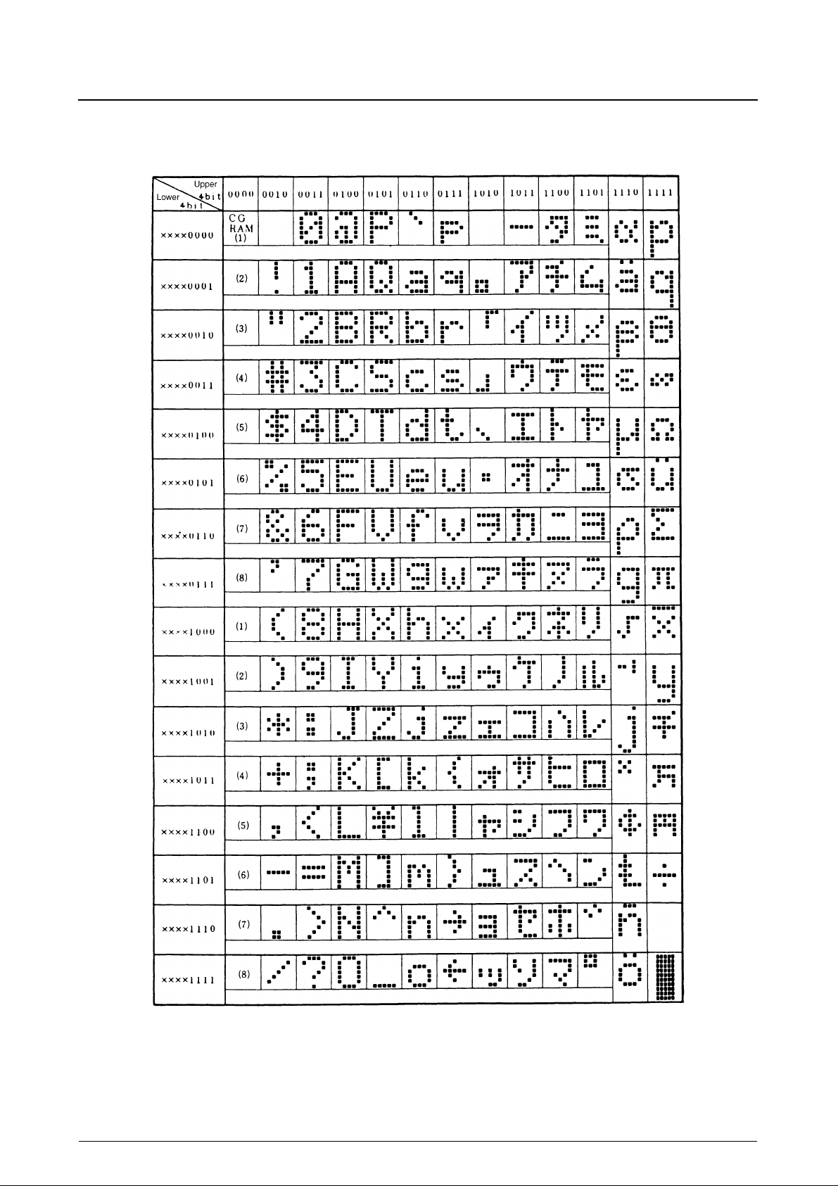
Character cord and the character bitmap
LC7986C
No. 4101—13/32
Page 14

5 × 7-pixel characters
LC7986C
The layout and addressing for 5 × 7-pixel characters is
shown in the following figure. Each character occupies
eight bytes, where bits 3 to 5 of the CG RAM address correspond to bits 0 to 2 of the character code. Note that bit 3
of the character code is not significant so, for example,
codes 00H and 08H select the same character.
Bits 0 to 2 of the CG RAM address are the bitmap row
address, where row 000 is the topmost displayed row.
The cursor, when displayed, is formed by ORing the bottom row with all 1s. If the cursor is used, row 111 should
contain all 0s so the cursor does not obscure the bottom
row of the character.
Bits 0 to 4 of the CG RAM data contain the character bitmaps. When a bit is 1, the corresponding pixel is ON, and
when 0, the pixel is OFF.
Bits 5 to 7 of the CG RAM data are present in memory, b ut
are not used by the display circuit. These bits can be used
as general-purpose RAM.
No. 4101—14/32
Page 15

5 × 10-pixel characters
LC7986C
The layout and addressing for 5 × 10-pixel characters is
shown in the following figure. Each character occupies
eleven bytes, where bits 4 and 5 of the CG RAM address
correspond to bits 1 and 2 of the character code. Note that
bits 0 and 3 of the character code are not significant so, for
example, codes 00H, 01H, 08H and 09H all select the same
character.
Bits 0 to 3 of the CG RAM address are the bitmap row
address where row 000 is the topmost displayed row.
The cursor, when displayed, is formed by ORing the bottom row with all 1s. If the cursor is used, row 1010 should
contain all 0s so the cursor does not obscure the bottom
row of the character.
Bits 0 to 4 of the CG RAM data contain the character bitmaps. When a bit is 1, the corresponding pixel is ON, and
when 0, the pixel is OFF.
Bits 5 to 7 of the CG RAM data are present in memory,
but are not used by the display circuit. These bits and the
CG RAM bytes, rows 1011 to 1111 that are not used by
the display circuit, can be used as general-purpose RAM.
Timing Generator
This circuit generates timing signals both for internal circuit operation and for driving external LC7930Ns. The
timing signals for the DD RAM, CG ROM and CG RAM
are independent of the microcontroller interface so that
memory accesses by the microcontroller do not cause
interference with the display drive signals.
No. 4101—15/32
Page 16

Display Drivers
LC7986C
The LC7986C incorporates 16 LCD common driver outputs and 80 LCD segment driver outputs. The character
font and the number of display lines determine the number
of active common outputs.
The segment drivers function identically to the LC7930N
segment drivers. The character bitmap data to be displayed
is latched in the internal 80-bit shift register before being
output on the segment drivers.
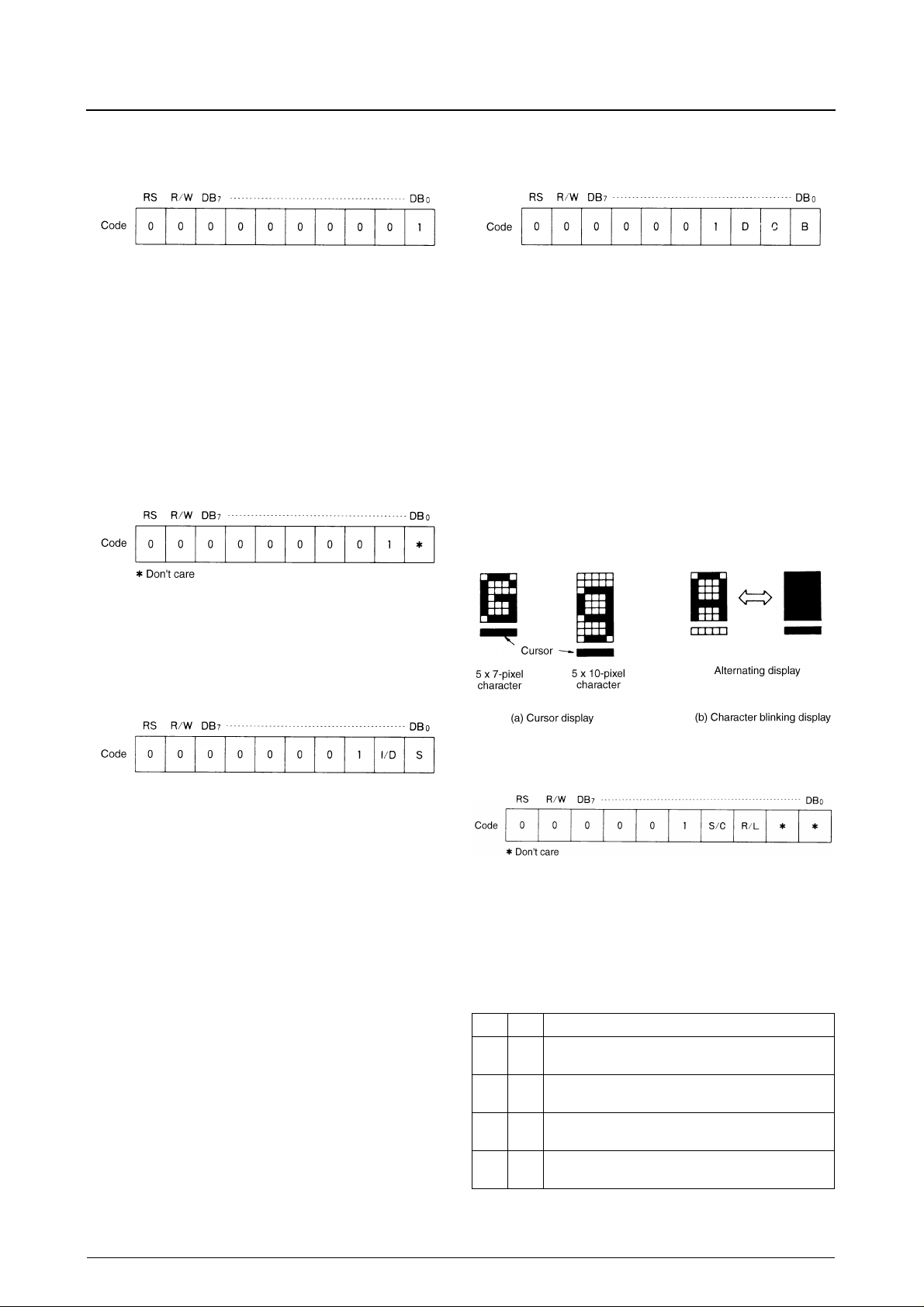
Cursor Display and Blinking
Cursor display and blinking of the character at the cursor
position are controlled using the Display ON/OFF instruction. The cursor position is at the character corresponding
to the address counter value as shown in the following fig-
The display bitmap data for each pixel-row is generated
starting with the left-most or the right-most pixel. The
shift direction is set using SHL. The data shifts through the
shift register and is output on the shift register serial data
output. The shift register latches the last 80 bits in the row
so the LC7986C displays the last 16 characters. External
LC7930Ns connect in series to the serial data output and
each one latches and displays bitmap data for eight additional characters.
ure. Note that the cursor and blinking character are also
displayed at the address counter value when CG RAM is
selected.
No. 4101—16/32
Page 17

LC7986C
Microcontroller Interface
DB0 to DB7 are used for the 4-bit data bus. Two read or
write cycles, therefore, are required to transfer each data,
status or instruction byte. The high-order four bits—bits
DB4 to DB7 in 8-bit interface mode—are transferred first.
The low-order four bits are then transferred as shown in
the following figure.
Reset Circuit
The internal reset circuit initializes the LC7986C at
power-ON. The busy flag remains ON from power-ON
until initialization is complete 10ms after VDD reaches
4.5V. Note that if power supply conditions are such that
the internal reset circuit does not operate to initialize the
device, the LC7986C must be initialized using commands
from the microcontroller.
The initialization sequence is as follows.
1. Clear Display
2. Set Function (D/L = 1, N = 0, F = 0)
Sets 8-bit interface size, 1-line display size and 5 × 7pixel character font.
3. Cursor/Display Control (D = 0, C = 0, B = 0)
Sets the display, the cursor and character blinking OFF.
4. Set Entry Mode (I/D = 1, S = 0)
Sets address counter auto-increment and sets display
shift OFF.
No. 4101—17/32
Page 18

Instructions
LC7986C
The external microcontroller accesses two register—
instruction register and data register—to control the
LC7986C. So the microcontroller interface is independent
of the microcontroller clock frequency, the LC7986C
stores the instruction of data internally before executing it.
There are four types of instructions.
• Function set instructions such as display type or interface size set
• Address set instructions
• Data read and write instructions
• Other instructions
The Busy Flag/Address Read instruction is the only
instruction that can be executed while the LC7986C is
executing a previous instruction. Before transmitting any
other instruction, the microcontroller should either check
that the busy flag is OFF or else wait longer than the execution time of the previous instruction.
Data read and write instructions are usually the most frequently used instructions. For increased microcontroller
efficiency, a display shift and display data write can be
executed simultaneously. In addition, the address counter
automatically increments or decrements after either a data
read or data write instruction, which reduces the operations required by the microcontroller. Note that the increment or decrement occurs after the busy flag turns OFF.
The delay until the address counter updates is
t
= 1.5/fCP or t
ADD
ADD
= 1.5/f
, and is shown in the
OSC
following figure.
The instructions are shown in the following table. The instruction code comprises the RS, R/W and DB0 to DB7 signals.
Instruction
Display Clear 0000000001
Cursor Home 000000001
Set Entry Mode 00000001I/DS
Display ON/OFF 0000001DCB
Cursor/Display Shift 000001S/CR/L
Set Function 00001DLNF
Set CG RAM Address 0001 CG RAM address
Set DD RAM Address 0 0 1 DD RAM address
Busy Flag/Address Read 0 1 BF Address counter
Data Write 1 0 Write data Writes data to DD RAM or CG RAM. 31
Data Read 1 1 Read data Reads data from DD RAM or CG RAM. 31
Note: *1.The execution time depends on the operating frequency. For example, if fCP or f
RS R/W DB7 DB6 DB5 DB4 DB3 DB2 DB1 DB0
I/D =1:
increment
S =1:
accompanied by display shift
S/C=1:
display shift
R/L =1:
right shift
DL =1:
8-bit
N =1:
two rows
10-pixel characters
F =1:
5
×
internally operating
BF =1:
Code
I/D =0:
S/C =0:
R/L =0:
DL =0:
N =0:
F =0:
BF =0:
Clears the display and sets the address counter to DD RAM
address 0.
Sets the address counter to DD RAM address 0. Returns a shifted
×
display to the original position. Does not alter the DD RAM data
Sets cursor movement and display shift following a data read or
write. When I/D is 1, the cursor increments, and when 0,
decrements. When S is 1, the display also shifts.
When D is 1, the display is ON, and when 0, OFF. When C is 1, the
cursor is ON, and when 0, OFF. When B is 1, blinking of the
character at the cursor position is ON, and when 0, OFF.
××
××
decrement
cursor shift
left shift
4-bit
a row
7-pixel characters
5
×
open to instructions
= 270kHz, the execution time is 31µs × 320/270 = 37µs.
OSC
Moves the cursor or the display without altering the DD RAM data.
When S/C is 1, the display shifts, and when 0, the cursor moves.
When R/L is 1, the direction is right, and when 0, left.
When DL is 1, the interface size is eight bits, and when 0, four bits.
When N is 1, the display size is two lines, and when 0, a single line.
When F is 1, the font size is 5
Sets the CG RAM address. Data read and writes after this
instruction are to and from CG RAM.
Sets the DD RAM address. Data read and writes after this
instruction are to and from DD RAM.
Used during execution of other instructions, outputs the busy flag
state and the address counter value. The address counter is used
for both DD RAM and CG RAM.
DD RAM : display data RAM
CG RAM : character generator RAM
: CG RAM address
A
CG
A
: DD RAM address: corresponding to cursor address
DD
AC : address counter used for both DD RAM and CG RAM
Description
×
10 pixels, and when 0, 5 × 7 pixels.
Execution time
(f
CP
or f
µ
µ
OSC
1.28ms
1.28ms
31
31µs
31
31
31
31
s (t
ADD
s (t
ADD
*1
(max)
= 320kHz)
µ
s
µ
s
µ
s
µ
s
µ
s
µ
s
0
= 4.7µs)
= 4.7µs)
No. 4101—18/32
Page 19
LC7986C
Display Clear
Fills the DD RAM with space characters (20
), returns the
H
display to the unshifted position and sets the address
counter to zero, returning the cursor to the top-left display
position. The address counter increment/decrement mode
is set to increment. The character blinking and display
shift modes are not affected.
Note that if a custom character generator ROM is used, the
space character must correspond to the 20
character code
H
for the display to be cleared correctly.
Cursor Home
Display ON/OFF
Sets the display, the cursor and character blinking ON or
OFF.
When D is 1, the display is ON, and when 0, OFF. Setting
the display ON or OFF does not alter the address counter
or the DD RAM data.
When C is 1, the cursor is ON, and when 0, OFF. Setting
the cursor ON or OFF does not affect the cursor autoincrement and display shift modes.
When B is 1, the cursor and the character at the cursor
position blink, alternating between black (all pixels ON)
and the displayed character as shown in the following figure. When f
320ms, and when f
CP
or f
= 320kHz, the blink interval is
OSC
CP
or f
= 270kHz, 379.2ms.
OSC
Returns the display to the unshifted position and sets the
address counter to zero, returning the cursor to the top-left
display position. Does not alter the DD RAM data.
Set Entry Mode
Sets the cursor auto-increment direction and the display
shift mode and direction. When I/D is 1, the address
counter increments when data is read from or written to
either the DD RAM or the CG RAM, thereby shifting the
cursor right one character position. When I/D is 0, the
address counter decrements, shifting the cursor left.
When S is 1, display shift is ON, and the display also
shifts one character position to the right or left when data
is written to the DD RAM so that the cursor position relative to the display is unchanged. No display shift occurs
when data is read from the DD RAM or when data is read
from or written to the CG RAM, although the address
counter increments or decrements for all read and write
operations. When S is 0, display shift is OFF.
Cursor/Display Shift
Shifts the cursor or the display either left or right as shown
in the following table. A DD RAM write is not required.
When shifting a 2-line display, both rows shift simultaneously, but characters do not move from one row to
another. Each time the display shifts, the characters in
each row only move within the row.
S/C R/L Description
00
01
10
11
Decrements the address counter and shifts the cursor left.
(–1 at AC)
Increments the address counter and shifts the cursor right.
(+1 at AC)
Shifts the display left. The address counter does not change,
and the cursor moves with the display.
Shifts the display right. The address counter does not change,
and the cursor moves with the display.
No. 4101—19/32
Page 20

LC7986C
Set Function
Sets the microcontroller interface bus size and the display
mode. When DL is 1, the interface size is eight bits, and
when 0, four bits. When the interface size is four bits, two
reads or writes of the high-order bits of the data bus, DB4
toB7, are required.
N and F set the display mode as shown in the following
table. N sets the number of lines in the display, and F, the
font size. Note that a 2-line display cannot use the 5 × 10pixel font size.
N F Display lines Font size (pixels) Duty
00 1 5
01 1 5
1 ×
25
7 1/8
10 1/11
7 1/16
Caution :
The font size and number of lines cannot be changed once
any other instruction is executed following the Set Function instruction.
has finished executing. When BF is 1, the previous instruction is executing, and when 0, the instruction has completed. The next instruction cannot be received until BF is
0. The microcontroller should, therefore, confirm that BF
is 0 before writing the next instruction.
The address counter is used for both the DD RAM and the
CG RAM. The address output on DB0 to DB7 is the
counter value before the currently executing instruction
began.
Data Write
Writes the 8-bit data on DB0 to DB7 to either the
DD RAM or the CG RAM, according to whether a Set
DD RAM Address or a Set CG RAM Address instruction
was executed previously. After writing, the address
counter automatically increments or decrements according
to the entry mode setting, and the display can also shift.
Data Read
Set CG RAM Address
Loads the 6-bit character generator RAM address into the
address counter. Data reads and writes after this instruction is executed are to and from the CG RAM.
Set DD RAM Address
Loads the 7-bit display data RAM address into the address
counter. Data reads and writes after this instruction is executed are to and from the DD RAM.
Busy Flag/Address Read
Outputs 8-bit data on DB0 to DB7 from either the
DD RAM or the CG RAM, according to whether a Set
DD RAM Address or a Set CG RAM Address instruction
was executed previously. After the data is read, the address
counter automatically increments or decrements according
to the entry mode setting, but the display does not shift.
Note that a Set DD RAM Address or Set CG RAM
Address instruction should be executed before executing
this command. If a Data Read instruction is executed without first executing an address set instruction, the output
data will not be valid. If the instruction is repeated, however, the output data will be valid data from the next
address. Subsequent Data Read instructions will output
valid data.
The output data will not be valid if this command is executed following a Data Write command, even though the
address counter has just incremented or decremented.
A Cursor/Display Shift instruction has the same effect as a
Set DD RAM Address instruction. If a Cursor/Display
Shift instruction moves the cursor, an address set instruction does not have to be executed before the Data Read
instruction, and the data is read from the DD RAM.
×
×
×
Outputs the busy flag state and the address counter value.
The busy flag is used to check if the previous instruction
No. 4101—20/32
Page 21
LC7986C
Microcontroller Interface
The LC7986C interfaces to both 4-bit and 8-bit microcontrollers.
8-bit interface
DB0 to DB7 are used for the 8-bit data bus. The timing sequence for instruction write, instruction execution, and busy
flag checking is shown in the following figure.
4-bit interface
The timing sequence for instruction write, instruction execution and busy flag checking is shown in the following figure.
The busy flag is checked after transferring two 4-bit sets of data. The busy flag and address counter value are output as
two 4-bit words. Checking the busy flag, therefore, requires two read cycles so the low-order four bits of the address
counter value are flushed from the data buffer.
Note. IR7 and IR3 are the 7th and 3rd bit, respectively, of the instruction. AC3 is the 3rd bit of the address counter.
No. 4101—21/32
Page 22
LCD Interface
LC7986C
The number of common signals and the duty cycle for
each combination of font and display lines are shown in
the following table. One common signal is required for
each pixel-row in the character, and an additional common
signal is required for the cursor row beneath the character.
Display lines Font size
7-pixel +
1
1
2
5
cursor
10-pixel +
5
cursor
5 × 7-pixel +
cursor
Sample Application Circuits
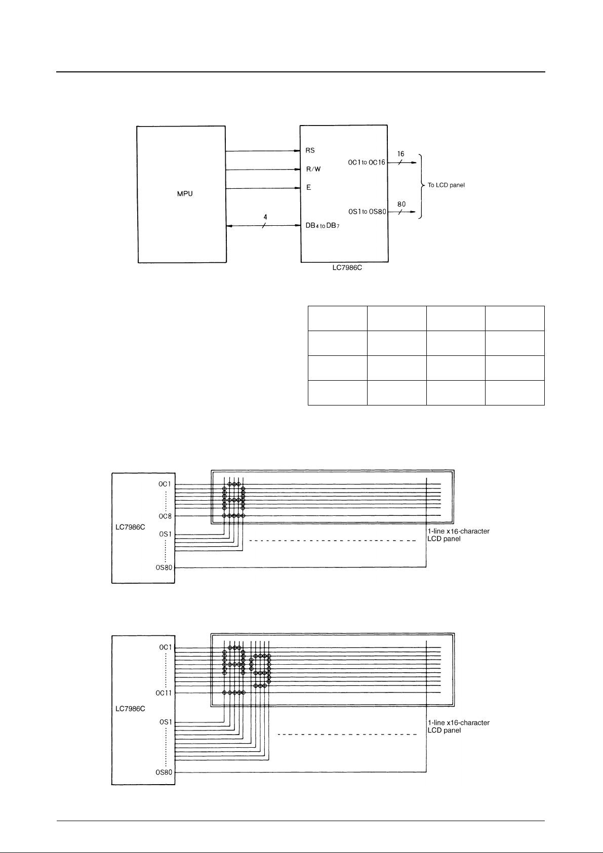
1-line × 16-character, 1/4-bias and 1/8-duty Display with 5 × 7-pixel Font
1-line × 16-character, 1/4-bias and 1/11-duty Display with 5 × 10-pixel Font
Common
signals
8 1/8
11 1/11
16 1/16
Duty
×
×
No. 4101—22/32
Page 23
LC7986C
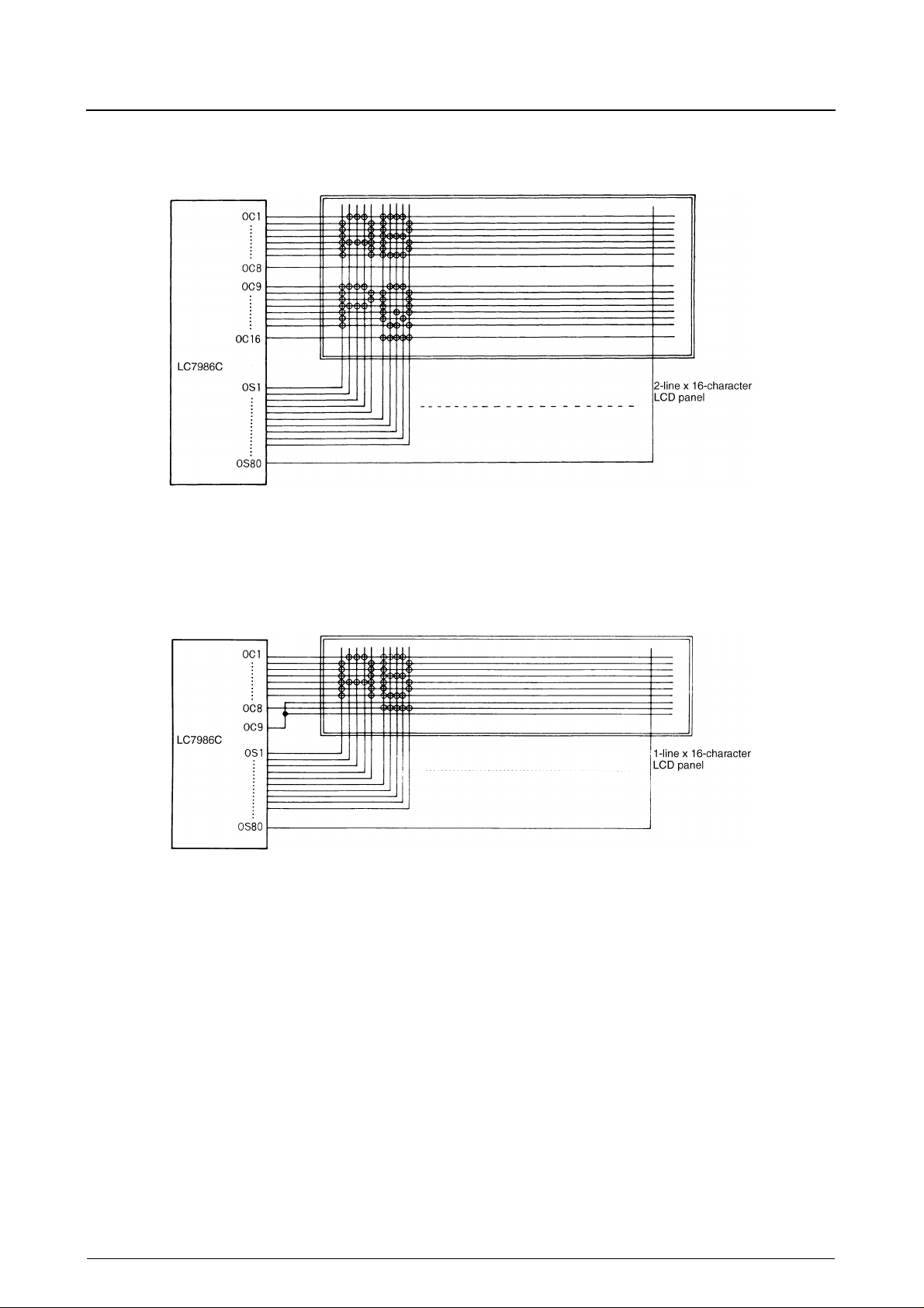
2-line × 16-character, 1/5-bias and 1/6-duty Display with 5 × 7-pixel Font
Connecting Unused Display Rows
Connecting unused LCD panel common pins to an unused LC7986C common output pin as shown in the following figure prevents crosstalk from the active drive signals affecting the display.
1-line × 16-character, 1/4-bias and 1/8-duty Display with 5 × 7-pixel Font
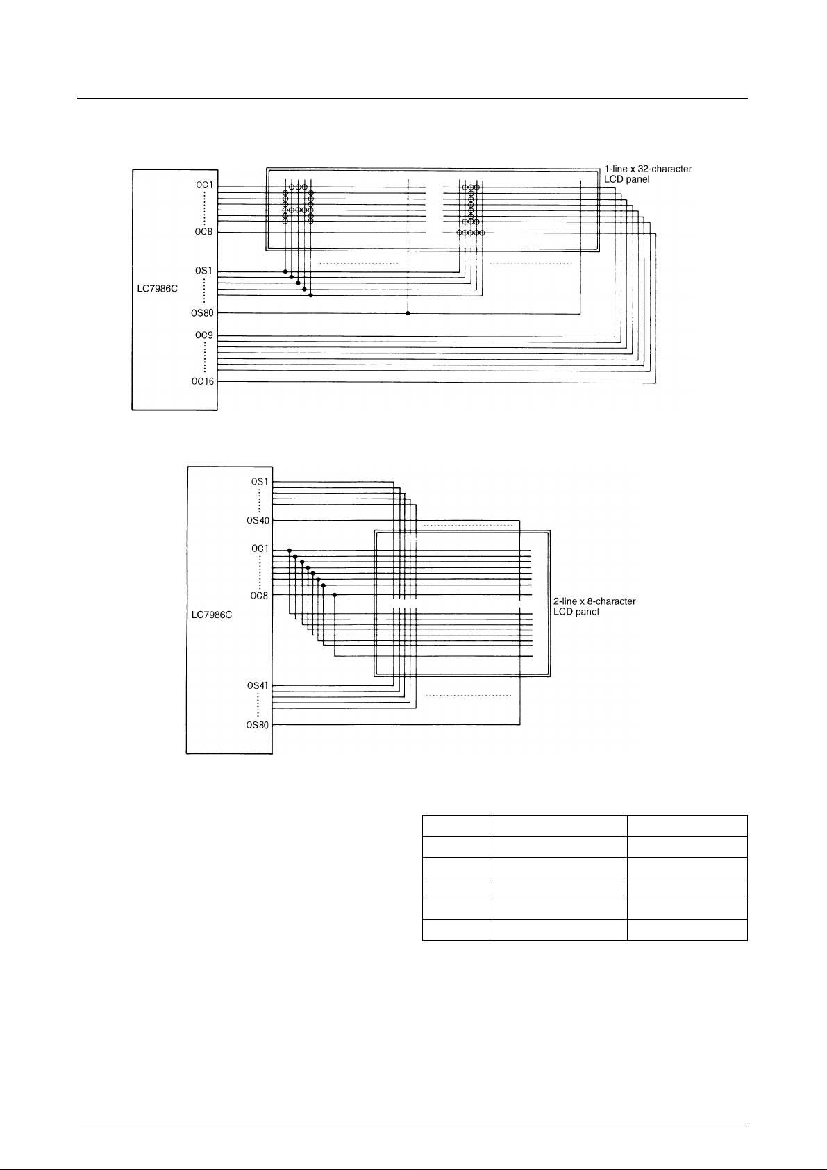
Alternative Display Connections
The LC7986C to LCD panel connections can be varied to match the LCD panel matrix as shown in the following sections.
No. 4101—23/32
Page 24
LC7986C
1-line × 32-character, 1/5-bias and 1/16-duty Display with 5 × 7-pixel Font
2-line × 8-character, 1/4-bias and 1/8-duty Display with 5 × 7-pixel Font
LCD driver power supply
The reference voltage levels required to generate the LCD
drive waveforms are shown in the following table.
Voltages V
to V
are input on pins V1 to V5, respectively.
1
5
The voltages can be produced using a voltage-divider
resistor network. The voltages required depend upon the
duty cycle. Connect V
to V4', V4 to V5' when using 1/5-bias drive. V
LCD driver peak voltage, where V
to V1', V1 to V2', V2 to V3', V3
DD
LCD
= V
DD
LCD
V
5
is the
.
The LCD drive wa v eforms are shown in the following sections. The calculations assume a 320kHz clock frequency
for a 4 µ s clock period.
Voltage 1/4 bias and 1/8 or 1/11 duty 1/5 bias and 1/16 duty
V
1
V
2
V
3
V
4
V
5
VDD − 0.25V
VDD − 0.5V
VDD − 0.5V
VDD − 0.75V
VDD − V
LCD
LCD
LCD
LCD
LCD
VDD − 0.2V
VDD − 0.4V
VDD − 0.6V
VDD − 0.8V
LCD
LCD
LCD
LCD
VDD − V
LCD
No. 4101—24/32
−
Page 25
A-type (A/B = HIGH)
1/8 duty LCD drive
1/11 duty LCD drive
LC7986C
1/16 duty LCD drive
No. 4101—25/32
Page 26

B-type (A/B = LOW)
1/8 duty LCD drive
1/11 duty LCD drive
LC7986C
1/16 duty LCD drive
No. 4101—26/32
Page 27

LC7930N Interface
LC7986C
When using a single-line display, up to eight LC7930Ns,
and when using a two-line display, up to three LC7930Ns
can interface to the LC7986C using the circuit shown in
the following figure. The LC7986C LOAD, CP, M and D
outputs connect directly to the LC7930Ns. Take care that
the V1 to V5 voltage reference outputs are connected correctly to the LC7930Ns.
No. 4101—27/32
Page 28
Examples
__L_
LC_
LC7986_
LC7986_
C7986 _
7986 L_
7986 LCD KO_
7986 LCD KO
7986 LCD KO
986 LCD CO
7986 LCD CO
7986 LCD CO_
7986 LCD CON_
LC7986 LCD CONTR
8-bit interface size, 1-line × 16-character display and
internal reset circuit
LC7986C
The programming example is shown in the following
table. This example assumes that the internal reset circuit
initializes the LC7986C.
The Set Function instruction that is executed before the
display is turned ON determines the operation of the
Since the DD RAM stores 80 characters, the display shift
function can be used as shown in the example. Note that
display shifts only change the display position and do not
alter the DD RAM. Using the Cursor Home instruction,
therefore, returns the display to its original position.
device.
Instruction
Power-ON
Set Function 00001100
Display ON/OFF 0000001110
Set Entry Mode 0000000110
Data Write 1001001100
Data Write 1001000011 Writes ‘C’.
RS R/W DB7 DB6 DB5 DB4 DB3 DB2 DB1 DB0
Code
××
Display Description
The internal reset circuit initializes the
LC7986C. The display is OFF.
Sets 8-bit interface size, 1-line display size and
×
7-pixel character font. The number of
5
display lines and the character font cannot be
changed later.
Turns the display ON and enables the cursor.
The display is blank.
Sets address auto-increment and automatic
cursor right shift on writing to DD RAM or
CG RAM. The display is not shifted.
Writes ‘L’ to DD RAM, since DD RAM was
selected when the LC7986C was initialized at
power-ON. The cursor position increments and
the cursor moves right.
Data Write
Data Write 1000110101 Writes ‘5’.
Set Entry Mode 0000000111 Sets display shift on writing to DD RAM.
Data Write 1000100000 Writes a space ‘ ’.
Data Write 1001001100 Writes ‘L ’.
Data Write
Data Write 1001001111 Writes ‘O’.
Cursor/Display Shift 00000100
Cursor/Display Shift 00000100
Data Write 1001000011
Cursor/Display Shift 00000111
Cursor/Display Shift 00000101
Data Write 1001001110 Writes ‘N.’
↓↓↓
↓↓↓
××
××
××
××
Shifts the cursor left.
Shifts the cursor left.
Writes ‘C’, the correct character. The display
scrolls left.
Shifts both the display and the cursor right.
Shifts the cursor right.
Data Write
Cursor Home 0000000010
↓↓↓
Sets both the display and the cursor position to
0.
No. 4101—28/32
Page 29

LC7986C
8-bit interface size, 1-line × 16-character display and microcontroller initialization
The initialization sequence for an LC7986C using an 8-bit interface is shown in the following figure.
Be sure to take this initialization because in some power supply conditions the internal reset circuit does not operate.
Power ON
Wait longer than 15ms after V
Wait longer than 4.1ms
Wait longer than 100µs
reaches 4.5V
DD
The busy flag cannot be tested before the
Function Set instruction sets the interface size.
The busy flag cannot be tested before the
Function Set instruction sets the interface size.
The busy flag cannot be tested before the
Function Set instruction sets the interface size.
The busy flag can be tested after executing the instructions below.
If the flag is not tested before writing another instruction, the microprocessor
should wait longer than the maximum instruction execution time.
Initialization complete
Function Set. Sets 8-bit interface size, the number of display lines and the character font. The
number of display lines and the character font cannot be changed after executing this instruction.
Display OFF
Display clear
Set entry mode
No. 4101—29/32
Page 30

8-bit interface size, 2-line × 16-character display and
__L_
LC7986_
LC7986
_
LC7986
L_
LC7986
LCD CONTROLLER&_
LC7986
LCD CONTROLLER&_
C7986
CD CONTROLLER&D_
LC7986
LCD CONTROLLER&D
internal reset circuit
LC7986C
The programming example is shown in the following
table.
Note that each row uses 40 bytes of DD RAM. When the
display is 16 characters long, to move the cursor from the
When shifting the display, both rows shift simultaneously
but characters do not move from one row to another. Each
time the display shifts, the characters in each row only
move within the row.
first row to the second, the DD RAM address should be
reset after the eighth character as shown in the example.
Instruction
Power-ON
Set Function 00001110
Display ON/OFF 0000001110
Set Entry Mode 0000000110
Data Write 1001001100
Data Write
RS R/W DB7 DB6 DB5 DB4 DB3 DB2 DB1 DB0
Code
××
↓↓↓
Display Description
The internal reset circuit initializes the
LC7986C. The display is OFF.
Sets 8-bit interface size, 2-line display size and
×
7-pixel character font.
5
Turns the display ON and enables the cursor.
The display is blank.
Sets address auto-increment and automatic
cursor right shift on writing to DD RAM or
CG RAM. The display is not shifted.
Writes ‘L’ to DD RAM, since DD RAM was
selected when the LC7986C was initialized at
power-ON. The cursor position increments and
the cursor moves right.
Data Write 1000110101 Writes ‘5’.
Set DD RAM Address 0011000000
Data Write 1001001100 Writes ‘L ’.
Data Write
Data Write 1001001111 Writes ‘O’.
Set Entry Mode 0000000111 Sets display shift on writing to DD RAM.
Data Write 1001001110
Data Write
Cursor Home 0000000010
↓↓↓
↓↓↓
Sets the DD RAM address to the first position
in the second row.
Writes ‘N. ’ The display scrolls left. The two lines
scroll simultaneously.
Sets both the display and the cursor position to
0.
No. 4101—30/32
Page 31

4-bit interface size, 1-line × 16-character display and
microcontroller initialization
LC7986C
The initialization sequence for an LC7986C using a 4-bit
interface is shown in the following figure.
The Function Set instruction is required to set the interface
size. With a 4-bit interface size, two write accesses are
required for each instruction. Since 8-bit interface size is
selected when the LC7986C is initialized at power-ON,
Power ON
Wait longer than 15ms
after VDD reaches 4.5V
The busy flag cannot be tested before the
Function Set instruction sets the interface size.
Wait longer than 4.1ms
the first write access is to an 8-bit interface on the
LC7986C. DB0 to DB3 are not connected, however, and
are not written. The Function Set instruction should therefore be repeated, writing DB4 to DB7 again and then DB0
to DB3, to initialize the device.
Wait longer than 100µs
The busy flag cannot be tested before the
Function Set instruction sets the interface size.
The busy flag cannot be tested before the
Function Set instruction sets the interface size.
The busy flag can be tested after executing the instructions below.
If the flag is not tested before writing another instruction, the microprocessor
should wait longer than the maximum instruction execution time.
The interface size is changed from 8-bit to 4-bit.
Function Set. Sets 8-bit interface size, the number of display lines and the character font. The
number of display lines and the character font cannot be changed after executing this instruction.
Display OFF
Display clear
Initialization complete
Set entry mode
No. 4101—31/32
Page 32

LC7986C
■
No products described or contained herein are intended for use in surgical implants, life-support systems, aerospace equipment, nuclear
power control systems, vehicles, disaster/crime-pre v ention equipment and the lik e, the failure of which may directly or indirectly cause injury,
death or property loss.
■
Anyone purchasing any products described or contained herein for an above-mentioned use shall:
➀
Accept full responsibility and indemnify and defend SANYO ELECTRIC CO., LTD., its affiliates, subsidiaries and distributors and all their
officers and employees, jointly and severally, against any and all claims and litigation and all damages, cost and expenses associated
with such use:
➁
Not impose any responsibility for any fault or negligence which may be cited in any such claim or litigation on SANYO ELECTRIC CO.,
LTD., its affiliates, subsidiaries and distributors or any of their officers and employees, jointly or severally.
■
Information (including circuit diagrams and circuit parameters) herein is for e xample only; it is not guaranteed for volume production. SANYO
believes information herein is accurate and reliable, but no guarantees are made or implied regarding its use or any infringements of
intellectual property rights or other rights of third parties.
This catalog provides information as of July, 1997. Specifications and information herein are subject to change without notice.
No. 4101—32/32
 Loading...