

Page 1
CMOS LSI
Ordering number : EN4349B
D3097HA (OT)/81096RM (OT)/21593JN (OT) No. 4349-1/5
SANYO Electric Co.,Ltd. Semiconductor Bussiness Headquarters
TOKYO OFFICE Tokyo Bldg., 1-10, 1 Chome, Ueno, Taito-ku, TOKYO, 110 JAPAN
Dot Matrix LCD Driver
LC79431D
Overview
The LC79431D is a large-scale dot matrix LCD common
driver LSI. The LC79431D contains an 80-bit
bidirectional shift register and a 4-level LCD driver. The
input/output pins for cascade connection can be used to
further increase the bit count. The LC79431D can be
used in conjunction with segment driver LC79400D or
LC79401D (QFP100D) to drive a wide-screen LCD
panel.
Features
• On-chip LCD drive circuit (80 bits)
• Display duty of 1/64 to 1/256 selectable
• On-chip input/output pins support a further increase in
bit count
• Supports externally supplied bias voltage
• Operating supply voltage/operating temperature are:
V
DD
(logic block) : 5 V ±10 % / –20 to +75 °C
VDD–VEE(LCD block) :
12 V to 32 V / –20 to +75°C
• CMOS process
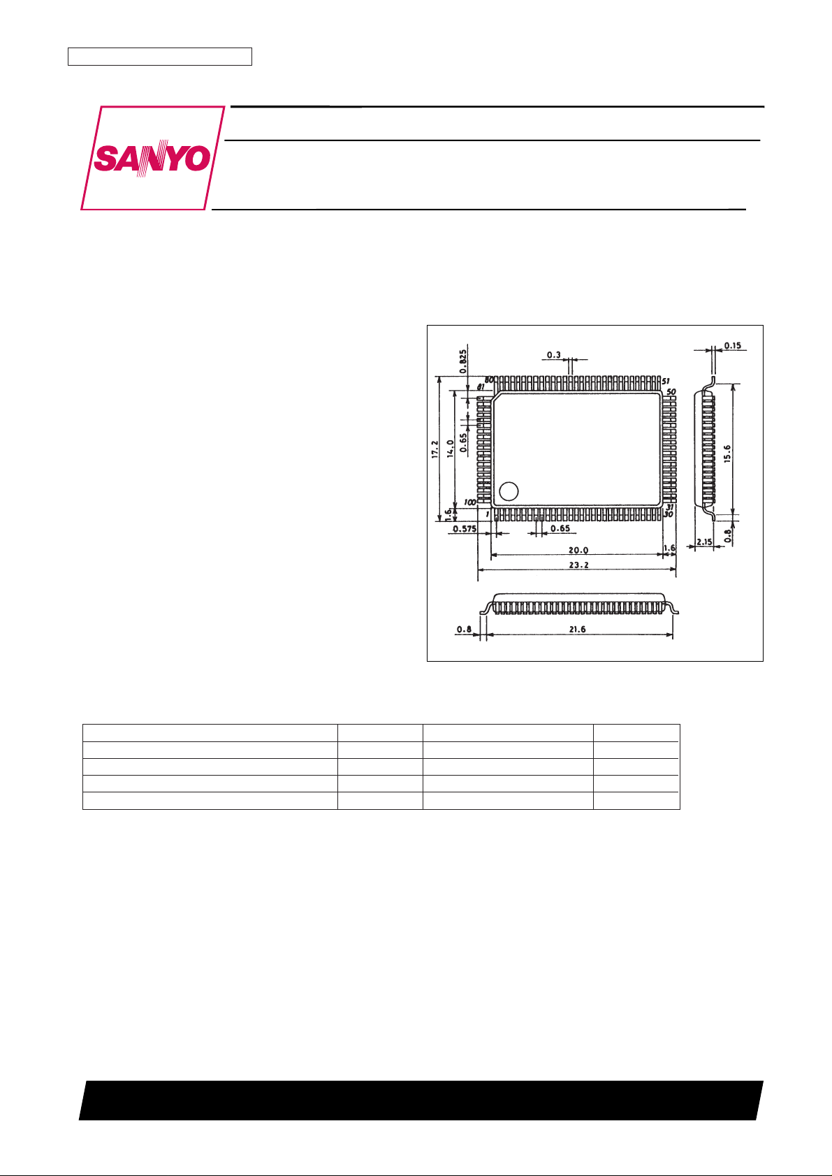
Package Dimensions
unit : mm
3180-QFP100D
[LC79431D]
SANYO: QIP100D
Specifications
Absolute Maximum Ratings at Ta = 25±2°C, VSS= 0V
Parameter Symbol Ratings Unit
Maximum supply voltage (logic) V
DD
max –0.3 to +7.0 V
Maximum supply voltage (LCD) V
DD0
– VEEmax * 0 to 35 V
Maximum input voltage V
IN
max –0.3 to VDD+0.3 V
Storage temperature range Tstg –40 to +125 °C
Note: * The voltages V1, V2, and V5 must obey the relationships: VDD≥ V1 > V2> V5 > VEE, VDD– V2 ≤ 7V, V5 – VEE≤ 7V.
Page 2
LC79431D
No. 4349-2/5
Allowable Operating Ranges at Ta = –20 to +75°C, VSS= 0V
Note: 1. The voltages V1, V2, and V5 must obey the relationships: VDD≥ V1 > V2 > V5 > VEE, VDD– V2 ≤ 7V, V5 – VEE≤ 7V.
2. When applying power, apply power to the LCD drive block after applying power to the logic block or apply power to both the blocks
simultaneously. When turning off power, turn off power to the logic block after turning off power to the LCD drive block or turn off power to both
the blocks simultaneously.
Electrical Characteristics at Ta = 25±2°C, VSS= 0V, VDD= 5V±10%
Note: * VDE= V1 or V2 or V5 or VEE, V1 = VDD, V2 = 16/17 (VDD– VEE), V5 = 1/17 (VDD– VEE)
Switching Characteristics at Ta = 25±2°C, VSS= 0V, VDD= 5V±10%
Parameter Symbol Conditions min typ max Unit
Supply voltage (logic) V
DD
4.5 5.5 V
Supply voltage (LCD) V
DD
– V
EE
*1, *2 12 32 V
Input high level voltage V
IH
DIO1, DIO80, CP, M, RS/LS,
0.8V
DD
V
DISP OFF
Input low level voltage V
IL
DIO1, DIO80, CP, M, RS/LS,
0.2V
DD
V
DISP OFF
CP (shift clock) f
CP
CP 1 MHz
CP (pulse width) t
WC
CP 63 ns
Setup time t
SETUP
DIO1 → CP, DIO80 → CP, 100 ns
Hold time t
HOLD
DIO1 → CP, DIO80 → CP, 100 ns
CP rise/fall time
t
R
CP 50 ns
t
F
CP 50 ns
Parameter Symbol Conditions min typ max Unit
Output delay time
t
PLH
CL= 15pF; CP → DIO1, CP → DIO80 250 ns
t
PHL
CL= 15pF; CP → DIO1, CP → DIO80 250 ns
Parameter Symbol Conditions min typ max Unit
Input high level current I
IH
V
IN
= VDD, VDD= 5.5 V; DIO1, DIO80,
1 µA
CP, M, RS/LS, DISP OFF
Input low level current I
IL
VIN= VSS, VDD= 5.5 V; DIO1, DIO80,
–1 µA
CP, M, RS/LS, DISP OFF
Output high level voltage V
OH
IOH= – 0.4 mA, VDD= 4.5 V;
V
DD
–0.4 V
DIO1, DIO80
Output low level voltage V
O
L
IOL= 0.4 mA, VDD= 4.5 V;
0.4 V
DIO1, DIO80
R
ON
(1)
V
DD
– VEE= 30 V, V
DE
– Vo = 0.5V
1.0 kΩ
Drive-on resistor
VDD= 4.5 V *; O1 to O80
R
ON
(2)
Vv– V
EE
= 20 V, V
DE
– Vo = 0.5V,
1.0 kΩ
V
DD
= 4.5 V *; O1 to O80
Current drain (1) I
SS
VDD–VEE= 30 V, CP = 14 kHz,
100 µA
no load, V
DD
= 5.5 V; V
SS
Current drain (2) I
EE
V
DD
– VEE= 30V, CP = 14 kHz,
100 µA
no load, V
DD
= 5.5 V; V
EE
Input capacitance C
IN
f
= 1 MHz; CP
5 pF
Page 3

LC79431D
No. 4349-3/5
Pin Assignment
Equivalent Circuit Block Diagram
Page 4

Pin Descriptions
Pin No Pin name Input/Output Functions
90 V
DD
VDDto VSS: Power supply for logic block
92 V
SS
Power supply
84 V
EE
VDDto VEE: Power supply for LCD drive block
87 V1 LCD drive level power supply
86 V2 Power supply V1 to V
EE
: Select level
85 V5 V2 to V5 : Nonselect level
96 CP Input Bidirectional shift register’s shift clock (triggering on the trailing edge)
98 DIO1 Input/Output
82 DIO80 Input/Output
91 RS/LS Input
94 M Input LCD drive output alternating signal
89 DISP OFF Input O1 to O80 output controlling input pin
1 O1 LCD drive output
The combination of scanning data, M signal, and DISP OFF signal can be
used to create output levels as shown below.
Output
80 O80 * Don’t care (To be set to either “H” or “L”)
LC79431D
No. 4349-4/5
M Data DISP OFF Output
L L H V2
L H H V
EE
H L H V5
H H H V1
* * L V1
RS/LS Data Transfer Direction DIO1 DIO80
L(Shift right) O1 → O80 IN OUT
H (Shift left)
O80 → O1 OUT IN
Page 5

LC79431D
No. 4349-5/5
Switching Characteristics Diagram
This catalog provides information as of December, 1997. Specifications and information herein are subject to
change without notice.
■ No products described or contained herein are intended for use in surgical implants, life-support systems, aerospace
equipment, nuclear power control systems, vehicles, disaster/crime-prevention equipment and the like, the failure of
which may directly or indirectly cause injury, death or property loss.
■ Anyone purchasing any products described or contained herein for an above-mentioned use shall:
➀ Accept full responsibility and indemnify and defend SANYO ELECTRIC CO., LTD., its affiliates, subsidiaries and
distributors and all their officers and employees, jointly and severally, against any and all claims and litigation and all
damages, cost and expenses associated with such use:
➁ Not impose any responsibility for any fault or negligence which may be cited in any such claim or litigation on
SANYO ELECTRIC CO., LTD., its affiliates, subsidiaries and distributors or any of their officers and employees
jointly or severally.
■ Information (including circuit diagrams and circuit parameters) herein is for example only; it is not guaranteed for
volume production. SANYO believes information herein is accurate and reliable, but no guarantees are made or implied
regarding its use or any infringements of intellectual property rights or other rights of third parties.
 Loading...