

Page 1
Ordering number: EN 6159
Overview
The LC7942YC is a common driver IC for driving large,
dot–matrix LCD displays. It features a built–in 64–bit
bidirectional shift register and a 4–level LCD driver. It can
also be connected in cascade to increase the number of
bits.
The LC7942YC is designed to be used with LC7940YC or
LC7941YC segment drivers to drive large LCD panels.
CMOS IC
LC7942YC
Dot-matrix LCD Driver
Features
• 64 built–in LCD display drive circuits
• l/64 to 1/128 display duty cycle
• Input/outputs for cascade connection
• Bias supply voltages can be supplied externally
• Operating supply voltage and ambient temperature
- 2.7 to 5.5V logic supply (VDD) at Ta = –20 to +85 °C
- 8 to 20 V LCD supply (VDD – VEE) at Ta = –20 to
+85 °C
• CMOS process
■ Any and all SANYO products described or contained herein do not have specifications that can handle
applications that require extremely high levels of reliability, such as life-support systems, aircraft’s
control systems, or other applications whose failure can be reasonably expected to result in serious
physical and/or material damage. Consult with your SANYO representative nearest you before using
any SANYO products described or contained herein in such applications.
■ SANYO assumes no responsibility for equipment failures that result from using products at values that
exceed, even momentarily, rated values (such as maximum ratings, operating condition ranges, or other
parameters) listed in products specifications of any and all SANYO products described or contained
herein.
SANYO Electric Co., Ltd. Semiconductor Company
TOKYO OFFICE Tokyo Bldg., 1-10, 1 Chome, Ueno, Taito-ku, TOKYO, 110-8534 JAPAN
63099RM (ID) No. 6159—1/8
Page 2
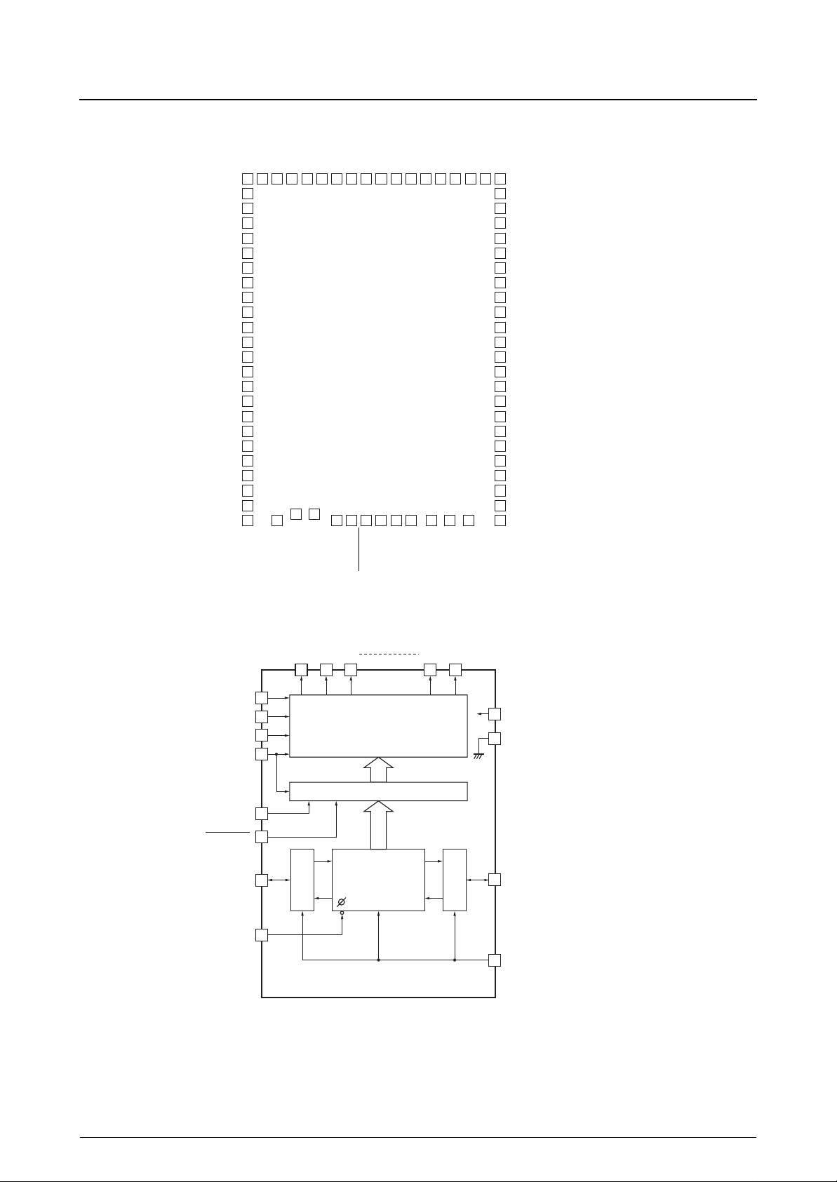
Pad Layout (Top view)
O41
O42
O43
O44
O45
O46
O47
O48
O49
O50
O51
O52
O53
O54
O55
O56
O57
O58
O59
O60
O61
O62
O63
O64
O40
O39
O38
DIO64
O37
VEE
O36
O35
O34
LC7942YC
V2
V1
V5
LC7942YC
O33
O32
O31
VDD
RS/LS
DISPOFF
O30
VSS
O29
M
O28
CP
O27
O26
DIO1
O25
O24
O23
O22
O21
O20
O19
O18
O17
O16
O15
O14
O13
O12
O11
O10
O9
O8
O7
O6
O5
O4
O3
O2
O1
Block Diagram
V1
V2
V5
VEE
DISP OFF
DIO1
CP
01 02 03 063 064
V
4 Level LCD Drive Circuit
(64 bits)
Level Shifter (64 bits)
M
Bidirectional
Shift Register
(64 bits)
I/OI/O
DD
V
SS
DIO64
RS/LS
No. 6159—2/8
Page 3
LC7942YC
LC7942YC Pad Location
chip size : 3.200 mm x 3.970 mm
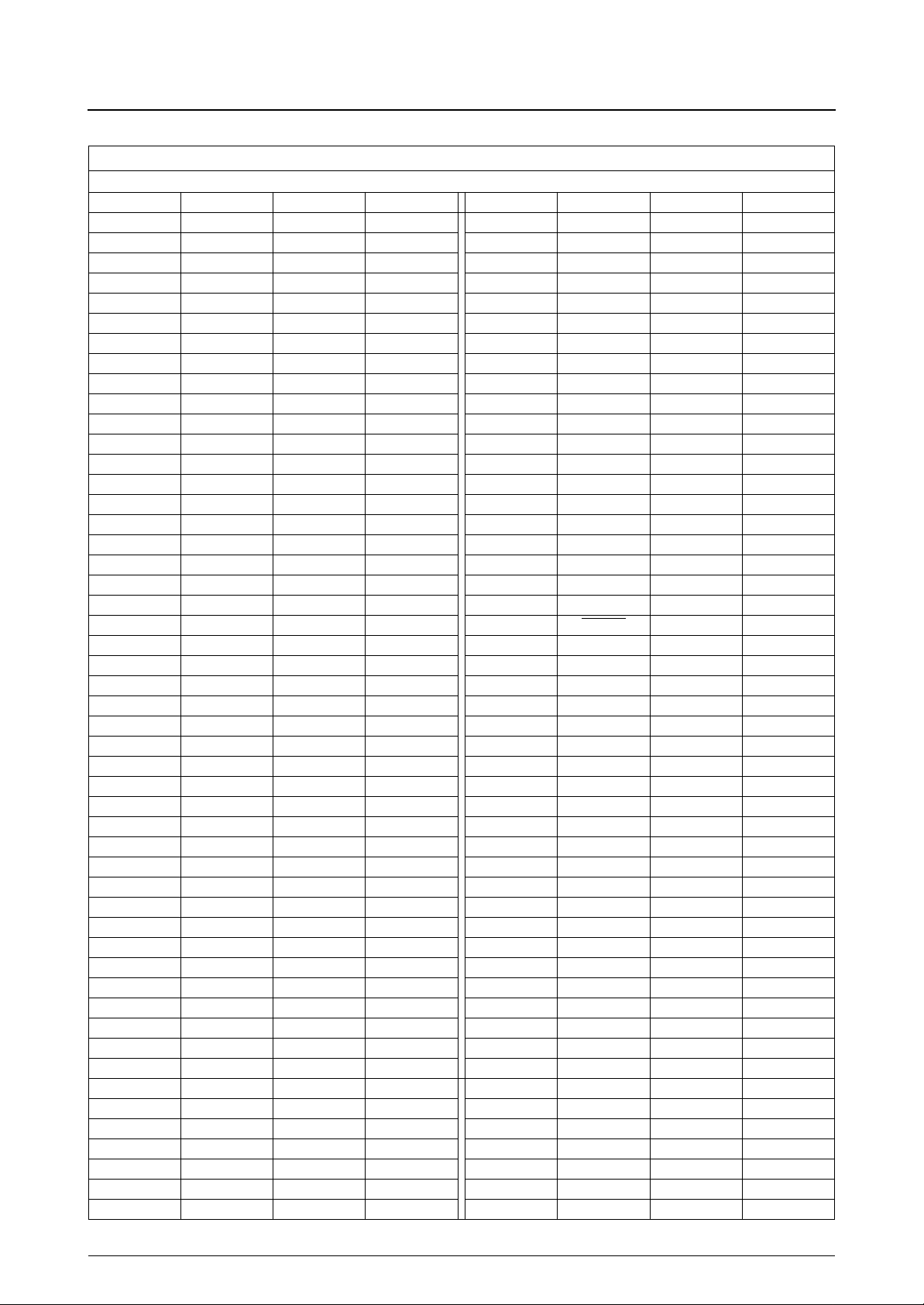
Pin_No. Name X Y Pin_No. Name X Y
41 O1 -1425.9 1808 11 O51 1425.9 -213
42 O2 -1425.9 1635 12 O52 1425.9 -70
43 O3 -1425.9 1465 13 O53 1425.9 70
44 O4 -1425.9 1298 14 O54 1425.9 213
45 O5 -1425.9 1134 15 O55 1425.9 359
46 O6 -1425.9 973 16 O56 1425.9 508
47 O7 -1425.9 815 17 O57 1425.9 660
48 O8 -1425.9 660 18 O58 1425.9 815
49 O9 -1425.9 508 19 O59 1425.9 973
50 O10 -1425.9 359 20 O60 1425.9 1134
51 O11 -1425.9 213 21 O61 1425.9 1298
52 O12 -1425.9 70 22 O62 1425.9 1465
53 O13 -1425.9 -70 23 O63 1425.9 1635
54 O14 -1425.9 -213 24 O64 1425.9 1808
55 O15 -1425.9 -359 25 DIO64 1096 1768
56 O16 -1425.9 -508 26 --- --- --57 O17 -1425.9 -660 27 V
58 O18 -1425.9 -815 28 V
59 O19 -1425.9 -973 29 V
60 O20 -1425.9 -1134 30 V
EE
5
2
1
61 O21 -1425.9 -1298 31 DISPOFF 143 1768
62 O22 -1425.9 -1465 32 V
DD
63 O23 -1425.9 -1635 33 RS/LS -213 1753
64 O24 -1425.9 -1808 34 V
SS
65 O25 -1236 -1808 35 --- --- --66 O26 -1053 -1808 36 M -598 1768
67 O27 -875 -1808 37 --- --- --68 O28 -704 -1808 38 CP -835 1768
69 O29 -538 -1808 39 --- --- --70 O30 -378 -1808 40 DIO1 -1056 1768
71 O31 -223 -1808
72 O32 -73 -1808
73 O33 73 -1808
74 O34 223 -1808
75 O35 378 -1808
76 O36 538 -1808
77 O37 704 -1808
78 O38 875 -1808
79 O39 1053 -1808
80 O40 1236 -1808
1 O41 1425.9 -1808
2 O42 1425.9 -1635
3 O43 1425.9 -1465
4 O44 1425.9 -1298
5 O45 1425.9 -1134
6 O46 1425.9 -973
7 O47 1425.9 -815
8 O48 1425.9 -660
9 O49 1425.9 -508
10 O50 1425.9 -359
880 1728
689 1728
498 1768
318 1768
-37 1753
-393 1753
No. 6159—3/8
Page 4

LC7942YC
Pin Functions
Number Name I/O Function
32 V
34 V
27 V
30 V
29 V
28 V
38 CP I Display data input clock (falling–edge trigger).
40 DIO1 I/O
25 DIO64 I/O
33 RS/LS I
36 M I LCD panel drive voltage output alternation control signal.
31 DISP OFF I O1 to O64 output control input pins.
41 to 80
1 to 24 O41 to O64
26 NC
35 NC
37 NC
39 NC
DD
SS
EE
1
2
5
O1 to O40
– Vss is the logic supply.
V
Supply
DD
VDD – VEE is the LCD supply.
LCD panel drive voltage supplies.
Supply
V1 and VEE are selected levels.
V2 and V5 are not–selected levels.
LOW (rlght shift) Input
HIGH (left shift) Output
LCD drive outputs
The output drive level is determined by the display data, M signal and DISPOFF input as show below.
O
Note
×
= don’t care (tied HIGH or LOW)
– No connection.
RS/LS DIO1
M Q DISPOFF Output
LOW LOW HIGH V
LOW HIGH HIGH V
HIGH LOW HIGH V
HIGH HIGH HIGH V
××
DIO64 Shift direction
Output O1
O64
Input O64 O1
2
EE
5
1
LOW V
1
Specifications
The following electrical characteristics apply when sealed in a Sanyo standard QIC-80 package.
Absolute Maximum Ratings at Ta = 25 ±2°C, V
Parameter Symbol Ratings Unit
Logic supply voltage VDD max –0.3 to +7.0
LCD supply voltage. See note. VDD – VEE max 0 to 22
Input voltage VI max –0.3 to VDD + 0.3
Operating temperature range T
Storage temperature range T
Note
V
≥ V1 > V2 >V5 > V
DD
EE
= 0 V
SS
opr
stg
–20 to +85
–40 to +125
V
V
V
°C
°C
No. 6159—4/8
Page 5

LC7942YC
Allowable Operating Ranges
Parameter Symbol Conditions
Logic supply voltage V
LCD supply voltage VDD – V
DIO1, DIO64, CP, M, RS/LS and
DISPOFF
HIGH–level input voltage
DIO1, DIO64, CP, M, RS/LS and
DISPOFF
LOW–level input voltage
CP shift clock frequency f
CP pulsewidth t
DIO1 and DIO64 to CP setup time t
DIOI and DIOS4 to CP hold time t
CP rise time t
CP fall time t
at Ta = –20 to +85 °C, V
DD
See notes 1 and 2. 8
EE
V
IH
V
IL
CP
WC
SETUP
HOLD
R
F
SS
= 0 V
Ratings
min typ max
2.7
–
–
0.8V
DD
––
––
0.2V
––
125
l00
l00
––
––
––
––
––
Unit
5.5 V
20 V
DD
1 MHz
50 ns
50 ns
ns
ns
ns
V
V
Notes
1. V
DD
V
> V
> V
1
> V
2
5
EE
2. At turn ON, the LCD supply should be energized after or simultaneously with the logic supply. At turn OFF, the logic supply
should be cut after or simultaneously with the LCD supply.
≥
Electrical Characteristics
Parameter Symbol Conditions
DIO1, DIO64, CP, M, RS/LS and
DISPOFF HIGH–level input current
DIO1, DIO64, CP, M, RS/LS and
DISPOFF
LOW–level input current
DIO1 and DIO64 HIGH–level output
voltage
DIO1 and DIO64 LOW–level output
voltage
O1 to O64 driver ON resistance R
VDD static supply current I
CP input capacitance C
Note
V
= V
or V
DE
or V5 or VEE, Vl = VDD, V2 = 10/11 × (VDD – VEE), V5 = l/11 × (VDD – VEE)
1
2
at Ta = 25 ± 2 C, V
I
IH
I
IL
V
OH
V
OL
ON
DD
I
VIN = V
DD
VIN = V
SS
IOH = –400 µA VDD – 0.4
IOL = 400 µA
VDD – VEE = 18 V,
VDD– V
OL
VDD = 4.5 V
VDD – VEE = 18 V,
CP = V
DD
fCP = 1 MHz
= 0 V, V
SS
= 0.25 V,
= 2.7 to 5.5 V
DD
Ratings
min typ max
––
–
1
––
1µA
––
––
––
––
–
5
0.4 V
1.5 k
100 µA
–
Unit
µA
V
Ω
pF
No. 6159—5/8
Page 6

LC7942YC
Switching Characteristics at Ta = 25 ± 2 °C, V
Parameter Symbol Conditions
t
Output delay time
PLH
t
PHL
CL = 30 pF
Switching Characteristics Waveform
twc
t
UP
SET
CP
DIO1
(DIO64)
t
R
= 0 V, VDD = 2.7 to 5.5 V
SS
t
F
0.2VDD
t
HOLD
t
PLH,tPHL
min typ max
––
––
DD
0.8V
Ratings
250
250
Unit
ns
DIO64
(DIO1)
No. 6159—6/8
Page 7

LCD Panel
LC7942YC
2
CP
LOAD
OD1 ED1
CP
SDI
LOAD
4
CP
SDI
LOAD
EE
V3V1M
V
V4
CP
SDI
LOAD
EE
V3V1M
V
V4
CP
SDI
LOAD
EE
V3V1M
V
V4
CP
SDI
LOAD
EE
V3V1M
V
V4
CDI
VEE
V3
V1
V4
LC7941YC
VEE
V4
VEE
V4
VEE
V4
(LC7940YC)
CDOCDI
LC7941YC
(LC7940YC)
CDOCDI
LC7941YC
(LC7940YC)
CDOCDI
LC7941YC
(LC7940YC)
M
V3
V1
M
V3
V1
M
V3
V1
M
1
2
159
160
161
162
319
320
321
322
LCD panel (640 × 200 pixels)
479
480
481
482
639
640
100
641
642
799
800
801
802
959
960
961
962
1119
1120
1121
1122
1279
1280
LC7940YC
LC7940YC
LC7940YC
LC7940YC
(LC7941YC)
M
(LC7941YC)
M
(LC7941YC)
M
(LC7941YC)
M
EE
V3
V
V1
V4
LC7941YC
EE
V3
V
V1
V4
LC7941YC
EE
V3
V
V1
V4
LC7941YC
EE
V3
V
V1
V4
LC7941YC
4
CP
LOAD
OD2 ED2
M
EE
V
4
V1 V3
V4
OD1
ED1
FLM
01
DI01
M
Mcontroller
064CP
DI064
LC7942YC
CL1
V2
V1
CL2
01
036CP
DI01
EE
4
V
V5
ED2
OD2
M
LC7942YC
VDD
EE
V2
V
V1
V5
V146V2
LA5311M
R
4
V3
V4
V5
–
+
–+–
–
+
R
+
R7RR
VEE
–11 to –13V
No. 6159—7/8
Page 8

LC7942YC
■ Specifications of any and all SANYO products described or contained herein stipulate the performance,
characteristics, and functions of the described products in the independent state, and are not guarantees
of the performance, characteristics, and functions of the described products as mounted in the customer’s
products or equipment. To verify symptoms and states that cannot be evaluated in an independent device,
the customer should always evaluate and test devices mounted in the customer’s products or equipment.
■ SANYO Electric Co., Ltd. strives to supply high-quality high-reliability products. However, any and all
semiconductor products fail with some probability. It is possible that these probabilistic failures could give
rise to accidents or events that could endanger human lives, that could give rise to smoke or fire, or that
could cause damage to other property. When designing equipment, adopt safety measures so that these
kinds of accidents or events cannot occur. Such measures include but are not limited to protective circuits
and error prevention circuits for safe design, redundant design, and structural design.
■ In the event that any or all SANYO products(including technical data,services) described or contained
herein are controlled under any of applicable local export control laws and regulations, such products
must not be exported without obtaining the export license from the author ities concerned in accordance
with the above law.
■ No part of this publication may be reproduced or transmitted in any form or by any means, electronic or
mechanical, including photocopying and recording, or any information storage or retrieval system, or
otherwise, without the prior written permission of SANYO Electric Co. , Ltd.
■ Any and all information described or contained herein are subject to change without notice due to
product/technology improvement, etc. When designing equipment, refer to the "Delivery Specification" for
the SANYO product that you intend to use.
■ Information (including circuit diagrams and circuit parameters) herein is for example only ; it is not
guaranteed for volume production. SANYO believes information herein is accurate and reliable, but no
guarantees are made or implied regarding its use or any infringements of intellectual proper ty rights or
other rights of third parties.
This catalog provides information as of June, 1999. Specifications and information herein are subject to
change without notice.
No. 6159—8/8
 Loading...