

Page 1
Ordering number: EN 6157
Overview
The LC7940YC and LC7941YC are segment driver ICs
for driving large, dot–matrix LCD displays. They read 4
bit parallel or serial input, display data from a controller
into an 80–bit latch, and then generate LCD drive signals
corresponding to that data.
The LC7940YC and LC7941YC feature mirror–image pin
assignments, allowing them to be used together to increase
component density. They are designed to be used with the
LC7942YC common driver to drive large LCD panels.
CMOS IC
LC7940YC,7941YC
Dot-matrix LCD Drivers
–
Features
• 80 built–in LCD display drive circuits
• 1/8 to l/128 display duty cycle
• Serial or 4–bit parallel data input
• Chip disable for low power dissipation for large–sized
panels
• Bias supply voltags can be supplied externally
• Operating supply voltage and ambient temperature
- 2.7 to 5.5 V logic supply ( VDD) at Ta = –20 to +85°C
- 8 to 20V LCD supply (V
–
VEE ) at Ta = –20 to
DD
+85 °C
• CMOS process
Specifications
The following electrical characteristics apply when sealed in a Sanyo standard QIC-100 package.
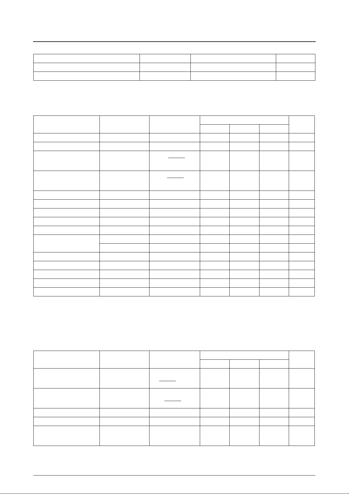
Absolute Maximum Ratings at Ta = 25 ± 2°C, V
Parameter Symbol Ratings Unit
Logic supply voltge VDD max –0.3 to +7.0
LCD supply voltage, See Note below. VDD – VEE max 0 to 22
Input voltage VI max –0.3 to VDD + 03
SS
= 0 V
V
V
°C
■ Any and all SANYO products described or contained herein do not have specifications that can handle
applications that require extremely high levels of reliability, such as life-support systems, aircraft’s
control systems, or other applications whose failure can be reasonably expected to result in serious
physical and/or material damage. Consult with your SANYO representative nearest you before using
any SANYO products described or contained herein in such applications.
■ SANYO assumes no responsibility for equipment failures that result from using products at values that
exceed, even momentarily, rated values (such as maximum ratings, operating condition ranges, or other
parameters) listed in products specifications of any and all SANYO products described or contained
herein.
SANYO Electric Co., Ltd. Semiconductor Company
TOKYO OFFICE Tokyo Bldg., 1-10, 1 Chome, Ueno, Taito-ku, TOKYO, 110-8534 JAPAN
63099RM (ID) No. 6157—1/13
Page 2
Parameter Symbol Ratings Unit
Operating temperature range
Storage temperature range
Note
V
≥ V1 > V3 > V4 > V
DD
EE
LC7940YC, LC7941YC
T
opr
T
stg
–20 to +85
–40 to +125
°C
°C
Recommended Operating Condltions at Ta =
Parameter Symbol Conditions
Logic supply voltage V
LCD supply voltage VDD – V
HIGH–level input voltage V
LOW–level inpvt voltage V
CP shift clock frequency f
CP pulsewidth t
LOAD pulsewidth t
DIn and SDI to CP setup time t
DIn and SDI to CP hold time t
CP to LOAD time
LOAD to CP time t
CP rise time t
CP fall time t
LOAD rise time t
LOAD fall time t
DD
IH
IL
CP
WC
WL
SETUP
HOLD
t
CL1
t
CL2
LC
R
F
RL
FL
EE
See Notes 1 and 2. 8 – 20
CP, CDl, DI1 to DI3, M,
SDl, P/S, DISPOFF and
LOAD
CP, CDI, Dl1 to DI3, M,
SDl, P/S,DISPOFF and
LOAD
–
20 to + 85°C, V
= 0V
SS
Ratings
min typ max
2.7 – 5.5
Unit
V
V
0.8V
DD
– – 0.2V
100––
100––
80––
80––
0––
100––
100––
––50
––50
––50
––50
––
DD
–3.3
V
V
MHz
ns
ns
ns
ns
ns
ns
ns
ns
ns
ns
ns
Notes
1. V
≥ Vl > V3 > V4 > V
DD
EE
2. At turn ON, the LCD supply should be energized after or simultaneously with the logic supply. At turn OFF, the logic supply
should be cut after or simultaneously with the LCD supply.
Electrlcai Characterfstlcs at Ta = 25 ± 2°C,V
Parameter Symbol Conditions
HIGH–level input current I
LOW–level input current I
CDO HIGH–level output voltage V
CDO LOW–levef output voltage V
O1 to O80 driver ON resistance RON
IH
IL
OH
OL
= 0V, VDD = 2.7 to 5.5 V
SS
Ratings
min typ max
VIN =VDD; LOAD, CP, CDI,
P/S, DI1 to DI3, SDl, M,
––1
and DISPOFF
VIN = VSS; LOAD, CP,
CDl, P/S, DI1 to DI3, SDI,
–––1
M, and DISPOFF
IOH = –400 µA VDD – 0.4 – –
IOL = 400 µA – – 0.4
VDD – VEE = 18 V,
|VDE – VO|= 0.25 V.
–24
See note
Unit
µA
µA
V
V
kΩ
No. 6157—2/13
Page 3
LC7940YC, LC7941YC
Parameter Symbol Conditions
CDI = VDD,
VDD to VSS standby supply current I
ST
VDD – VEE = 18 V,
fCP = 3.3 MHz,
no output load ; V
SS
VDD – VEE = 18 V,
VDD to Vss operating supply current I
SS
fCP = 3.3 MHz,
I
= 5.156 kHz,
LOAD
fM = 52 Hz ;VSS
VDD – VEE = 18V,
VDD to VEE operating supply current I
CP input capacitance C
EE
I
fCP = 3.3 MHz,
f
= 5,156 kHz,
LOAD
= 52 Hz ; V
f
M
EE
fCP = 3.3 MHz ; CP – 5 –
Note
V
= V1 or V3, or V4 or VEE, V1 = VDD, V3 = 9/11 × (VDD – VEE), V4 = 2/11 × (VDD – VEE)
DE
Switching Characteristics at Ta = 25 ± 2°C,V
Parameter Symbol Conditions
CDO output delay time t
D
= 0V, VDD = 2.7 to 5.5 V
SS
CL = 30 pF – – 200
Ratings
min typ max
– – 200
––1.0
––0.1
Ratings
min typ max
Unit
µA
mA
mA
pF
Unit
ns
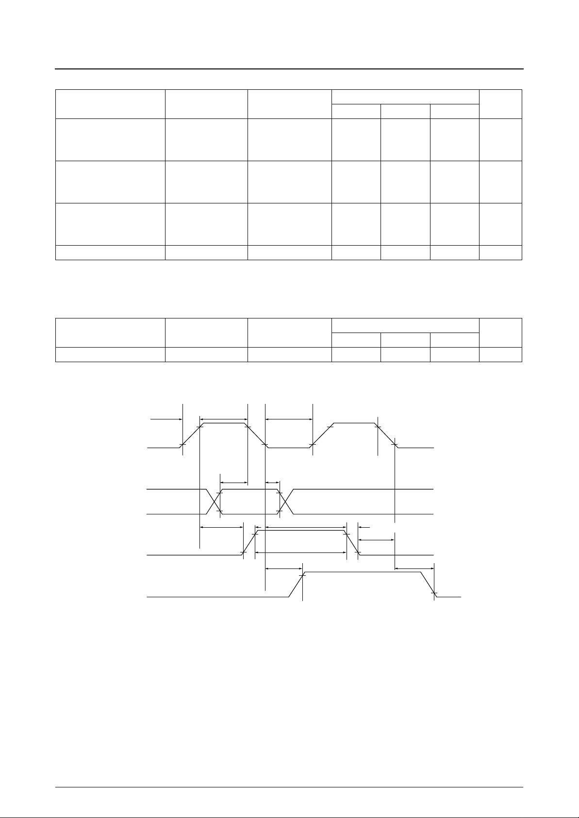
Switching Characteristics Waveform
t
t
CP
SDI
DI1 to 3
LOAD
CDO
WC
R
t
t
CL (1)
SET
UP
t
t
t
RL
WC
F
t
HOLD
t
CL (2)
t
WL
t
D
t
FL
0.8V
DD
0.2VDD
t
LC
t
D
No. 6157—3/13
Page 4
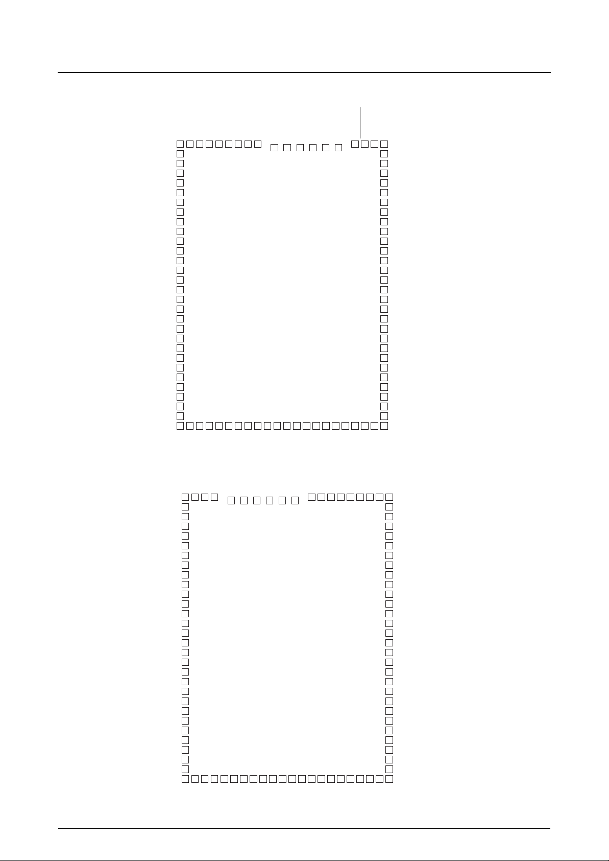
Pad Layout (Top view)
O1
O2
O3
O4
O5
O6
O7
O8
O9
O10
O11
O12
O13
O14
O15
O16
O17
O18
O19
O20
O21
O22
O23
O24
O25
O26
O27
O28
O29
O30
CP
O31
CDI
O32
LOAD
O33
LC7940YC, LC7941YC
SDI
DI3
DI2
DI1
M
V1
LC7940YC
O34
O35
O36
O37
O38
O39
O40
VDDV3V4
O41
O42
O43
O44
VEE
O45
VSS
O46
O47
P/S
DISPOFF
O48
O49
CDO
O50
O80
O79
O78
O77
O76
O75
O74
O73
O72
O71
O70
O69
O68
O67
O66
O65
O64
O63
O62
O61
O60
O59
O58
O57
O56
O55
O54
O53
O52
O51
O80
O79
O78
O77
O76
O75
O74
O73
O72
O71
O70
O69
O68
O67
O66
O65
O64
O63
O62
O61
O60
O59
O58
O57
O56
O55
O54
O53
O52
O51
CDO
DISPOFF
O50
O49
P/S
O48
O47
VSS
VEEV4V3
O46
O45
VDD
LC7941YC
O44
O43
O42
O41
V1
O40
O39
M
O38
DI1
O37
DI2
O36
DI3
O35
SDI
O34
LOAD
O33
CDI
O32
CP
O31
O1
O2
O3
O4
O5
O6
O7
O8
O9
O10
O11
O12
O13
O14
O15
O16
O17
O18
O19
O20
O21
O22
O23
O24
O25
O26
O27
O28
O29
O30
No. 6157—4/13
Page 5
LC7940YC, LC7941YC
LC7940YC Pad Location
chip size : 4.830 mm x 3.550 mm
Pin_No. Name X Y Pin_No. Name X Y
1 O1 -1600 2240 51 O51 1600 -2240
2 O2 -1600 2072 52 O52 1600 -2072
3 O3 -1600 1906 53 O53 1600 -1906
4 O4 -1600 1742 54 O54 1600 -1742
5 O5 -1600 1580 55 O55 1600 -1580
6 O6 -1600 1420 56 O56 1600 -1420
7 O7 -1600 1262 57 O57 1600 -1262
8 O8 -1600 1106 58 O58 1600 -1106
9 O9 -1600 952 59 O59 1600 -952
10 O10 -1600 800 60 O60 1600 -800
11 O11 -1600 650 61 O61 1600 -650
12 O12 -1600 502 62 O62 1600 -502
13 O13 -1600 356 63 O63 1600 -356
14 O14 -1600 212 64 O64 1600 -212
15 O15 -1600 70 65 O65 1600 -70
16 O16 -1600 -70 66 O66 1600 70
17 O17 -1600 -212 67 O67 1600 212
18 O18 -1600 -356 68 O68 1600 356
19 O19 -1600 -502 69 O69 1600 502
20 O20 -1600 -650 70 O70 1600 650
21 O21 -1600 -800 71 071 1600 800
22 O22 -1600 -952 72 O72 1600 952
23 O23 -1600 -1106 73 O73 1600 1106
24 O24 -1600 -1262 74 O74 1600 1262
25 O25 -1600 -1420 75 O75 1600 1420
26 O26 -1600 -1580 76 O76 1600 1580
27 O27 -1600 -1742 77 O77 1600 1742
28 O28 -1600 -1906 78 O78 1600 1906
29 O29 -1600 -2072 79 O79 1600 2072
30 O30 -1600 -2240 80 O80 1600 2240
31 O31 -1420 -2240 81 --- --- --32 O32 -1262 -2240 82 CDO 1415 2240
33 O33 -1106 -2240 83 --- --- --34 O34 -952 -2240 84 DISPOFF
35 O35 -800 -2240 85 P/S 1091 2240
36 O36 -650 -2240 86 V
37 O37 -502 -2240 87 V
38 O38 -356 -2240 88 V
39 O39 -212 -2240 89 V
SS
EE
4
3
40 O40 -70 -2240 90 --- --- --41 O41 70 -2240 91 V
42 O42 212 -2240 92 V
DD
1
43 O43 356 -2240 93 M -316 2240
44 O44 502 -2240 94 DI1 -467 2240
45 O45 650 -2240 95 DI2 -620 2240
46 O46 800 -2240 96 DI3 -775 2240
47 O47 952 -2240 97 SDI -932 2240
48 O48 1106 -2240 98 LOAD -1091 2240
49 O49 1262 -2240 99 CDI -1252 2240
50 O50 1420 -2240 100 CP -1415 2240
1252 2240
825 2179
629 2179
464 2179
299 2179
123 2179
-42 2179
No. 6157—5/13
Page 6
LC7940YC, LC7941YC
LC7941C Pad Location
chip size : 4.830 mm x 3.550 mm
Pin No. Name X Y Pin No. Name X Y
1 O80 -1600 2240 51 O30 1600 -2240
2 O79 -1600 2072 52 O29 1600 -2072
3 O78 -1600 1906 53 O28 1600 -1906
4 O77 -1600 1742 54 O27 1600 -1742
5 O76 -1600 1580 55 O26 1600 -1580
6 O75 -1600 1420 56 O25 1600 -1420
7 O74 -1600 1262 57 O24 1600 -1262
8 O73 -1600 1106 58 O23 1600 -1106
9 O72 -1600 952 59 O22 1600 -952
10 O71 -1600 800 60 O21 1600 -800
11 O70 -1600 650 61 O20 1600 -650
12 O69 -1600 502 62 O19 1600 -502
13 O68 -1600 356 63 O18 1600 -356
14 O67 -1600 212 64 O17 1600 -212
15 O66 -1600 70 65 O16 1600 -70
16 O65 -1600 -70 66 O15 1600 70
17 O64 -1600 -212 67 O14 1600 212
18 O63 -1600 -356 68 O13 1600 356
19 O62 -1600 -502 69 O12 1600 502
20 O61 -1600 -650 70 O11 1600 650
21 O60 -1600 -800 71 O10 1600 800
22 O59 -1600 -952 72 O9 1600 952
23 O58 -1600 -1106 73 O8 1600 1106
24 O57 -1600 -1262 74 O7 1600 1262
25 O56 -1600 -1420 75 O6 1600 1420
26 O55 -1600 -1580 76 O5 1600 1580
27 O54 -1600 -1742 77 O4 1600 1742
28 O53 -1600 -1906 78 O3 1600 1906
29 O52 -1600 -2072 79 O2 1600 2072
30 O51 -1600 -2240 80 O1 1600 2240
31 O50 -1420 -2240 81 CP 1415 2240
32 O49 -1262 -2240 82 CDI 1252 2240
33 O48 -1106 -2240 83 LOAD 1091 2240
34 O47 -952 -2240 84 SDI 932 2240
35 O46 -800 -2240 85 DI3 775 2240
36 O45 -650 -2240 86 DI2 620 2240
37 O44 -502 -2240 87 DI1 467 2240
38 O43 -356 -2240 88 M 316 2240
39 O42 -212 -2240 89 V
40 O41 -70 -2240 90 V
1
DD
41 O40 70 -2240 91 --- --- --42 O39 212 -2240 92 V
43 O38 356 -2240 93 V
44 O37 502 -2240 94 V
45 O36 650 -2240 95 V
3
4
EE
SS
46 O35 800 -2240 96 P/S -1091 2240
47 O34 952 -2240 97 DISPOFF -1252 2240
48 O33 1106 -2240 98 --- --- --49 O32 1262 -2240 99 CDO -1415 2240
50 O31 1420 -2240 100 --- --- ---
42 2179
-123 2179
-299 2179
-464 2179
-629 2179
-825 2179
No. 6157—6/13
Page 7
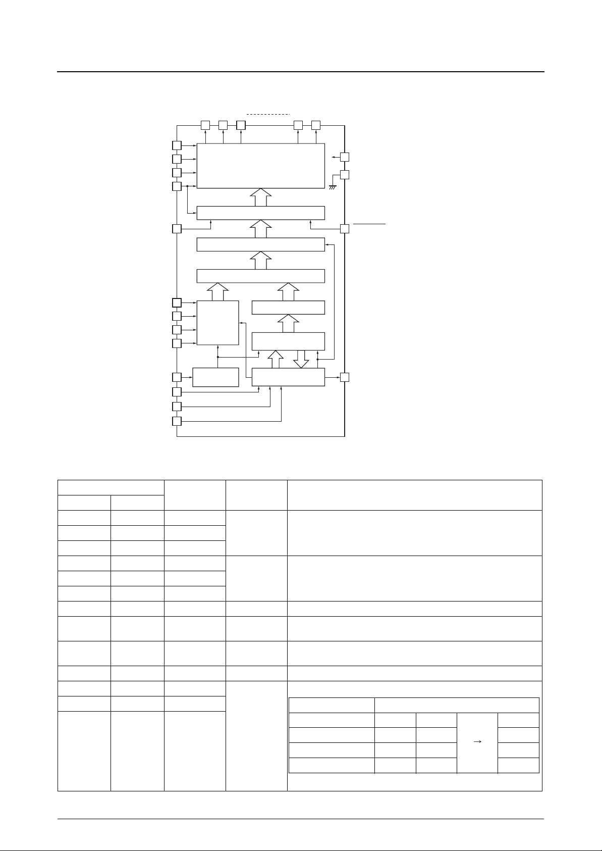
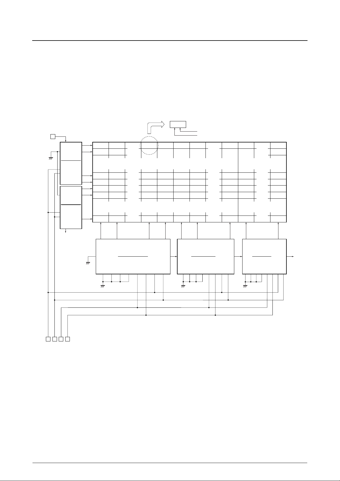
Block Diagram
LC7940YC, LC7941YC
01 02 03 079 080
V1
V3
V4
V
EE
M
4 Level LCD Drive Circuit
(80 bits)
80
Level Shifter (80 bits)
80
2nd Latch (80 bits)
80
1st Latch (80 bits)
VDD
SS
V
DISP OFF
SDI
DI3
DI2
DI1
P/S CDO
CDI
CP
LOAD
4 bits
Data Bus
Interface
SER/PAR
Control
CLK
204
Address Decoder
Address Counter
(7 bits)
Chip Disable &
Latch Control
Pin Functions
Pin No.
LC7940YC LC7941YC
91 90 V
86 95 V
87 94 V
92 89 V
89 92 V
88 93 V
l00 81 CP I Display data Input clock (falling–edge trigger).
99 82 CDI I
98 83 LOAD I
97 84 SDI I Serial data input.
96 85 DI3
95 86 DI2
94 87 D11
Symbol I/O Function
DD
SS
EE
Supply
1
3
4
Supply
V
– VSS is the logic supply.
DD
VDD – VEE is the LCD supply.
LCD panel drive voltage supplies
V1 and VEE are selected levels.
V3 and V4 are not–selected levels.
Chip disable.
Data is read in when LOW, and not road in when HIGH.
Display data latch clock (falling–edge trigger).
On the falling edge, the LCD drive signals set by the display data are output.
4–bit parallel data input pins.
Data input LCD driver outputs
SDI O4 O8
I
DI3 O3 O7 O79
DI2 O2 O6 O78
DI1 O1 O5 O77
O80
In serial data input mode, DI1 to DI3 should all be tied HIGH or LOW.
No. 6157—7/13
Page 8

LC7940YC, LC7941YC
Pin No.
LC7940YC LC7941YC
Symbol I/O Function
93 88 M I LCD panel drive voltage output alternation control signal.
85 96 P/S I Data input mode select. 4–bit parallel input when HIGH, and serial input when LOW
82 99 CDO O
Cascade connection pin for extension segment drivers. Data is read out when HIGH.
Goes LOW after data is read out. Connected to the CDI input of the next chip.
LCD drive outputs.
The output drive level is determined by the display data, M signal and DISP OFF
input as shown below.
M Q DISP OFF Output
LOW LOW HIGH V
1 to 80 80 to 1 Ol to O80 O
LOW HIGH HIGH V
HIGH LOW HIGH V
HIGH HIGH HIGH V
××
LOW V
Note
x = don’t care (tied HIGH or LOW)
84 97 DISPOFF
I
O1 to O80 output control input pin.
When LOW, V1 is output on the O1 to 080 outputs, See the truth table.
81 91 NC
– No connection.83 98 NC
90 100 NC
3
1
4
EE
1
No. 6157—8/13
Page 9
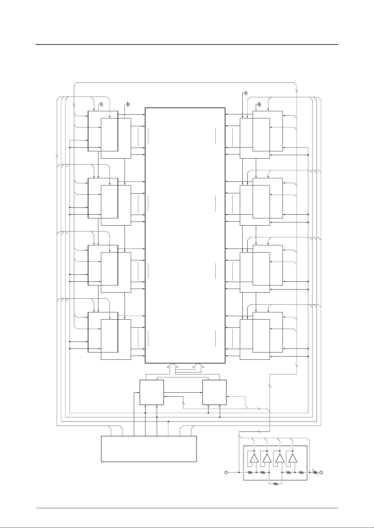
Application Notes
LCD Panel 1
4
CP
SDI
LOAD
V3V1M
CP
LOAD
OD1 ED1
2
CP
SDI
LOAD
V3V1M
CP
SDI
LOAD
V3V1M
CP
SDI
LOAD
V3V1M
LC7940YC, LC7941YC
CP
SDI
LOAD
CDI
EE
V
VEE
V3
V4
V1
V4
LC7941YC
VEE
V4
VEE
V4
VEE
V4
(LC7940YC)
CDOCDI
LC7941YC
(LC7940YC)
CDOCDI
LC7941YC
(LC7940YC)
CDOCDI
LC7941YC
(LC7940YC)
M
EE
V
V3
V4
V1
M
EE
V
V3
V4
V1
M
EE
V
V3
V4
V1
M
1
2
159
160
161
162
319
320
321
322
LCD panel (640 × 200 pixels)
479
480
481
482
639
640
100
641
642
799
800
801
802
959
960
961
962
1119
1120
1121
1122
1279
1280
LC7940YC
LC7940YC
LC7940YC
LC7940YC
(LC7941YC)
M
(LC7941YC)
M
(LC7941YC)
M
(LC7941YC)
M
EE
V3
V
V1
V4
LC7941YC
EE
V3
V
V1
V4
LC7941YC
EE
V3
V
V1
V4
LC7941YC
EE
V3
V
V1
V4
LC7941YC
4
CP
LOAD
OD2 ED2
M
EE
V
4
V1 V3
V4
OD1
ED1
FLM
01
DI01
M
M
controller
064CP
DI064
LC7942YC
CL1
V2
V1
CL2
01
036CP
DI01
EE
4
V
V5
ED2
OD2
LC7942YC
M
VDD
EE
V2
V
V1
V5
V146V2
LA5311M
R
4
V3
V4
V5
+
–
+
+
–
+
–
R
–
R7RR
VEE
–11 to –13V
No. 6157—9/13
Page 10

LCD Panel 2
LC7940YC, LC7941YC
42
4
2 4
EE
V4 V
M V1 V3
CP
LOAD
4bit Data
CDI
080 01
CDO
CDICDO
080 01
4bit Data
CP LOAD
LC7941YC-#1
EE
V3
V
V1
V4
M
24244
LC7941YC-#2 LC7941YC-#1
24
LC7941YC-#2
24
LCD panel (640 × 200 pixels)
2
LC7941YC-#8
24
LC7941YC-#8
4bit Data
100
DI01
01
M
036CP
LC7942YC-#2
VDD
EE
V2
V
V1
V5
V146V2
LA5311M
R
V3
–
–
+
+
R
100
01
064CP
4
4bit Data
FLM
DI01
M
M
controller
LC7942YC-#1
CP
LOAD
EE
4
V
V1 V3
V4
EE
V
4
–11 to –13V
4
V4
V5
–
–
+
+
R
R
7R
No. 6157—10/13
Page 11
LC7940YC, LC7941YC
100 x 240-pixel LCD Panel Application
A 100 × 240
pixel LCD panel requires the following
–
drivers.
• 3 x LC7940YC (or LC7941YC) drivers
• 2 x LC7942YC drivers
An example using l/l00 duty cycle is shown below.
Frame Signal
1,2
DI01 01
RS/LS 02
LC7942YC
#1
CP
M
063
DI064 064
DI01 01
RS/LS 02
LC7942YC
#2
CP
M
036
DI064
O37 to O64
are open.
1,1
2,1
--- ---
63,2
63,1
64,2
64,1
65,2
65,1
66,2
66,1
100,2
100,1
01
---
2,2
--- ---
---
---
---
02
LCD Panel (100 × 240 pixels)
100,79
1,79
1,80
64,80
65,80
100,80
079#1080
1,79
1,81
64,81
65,81
100,81
01 02
(m,n) : pixel address
Segment line (n)
Common line (m)
1,82
---
---
---
100,82
---
1,160
64,160
65,160
100,160
080
1,
161
--- ---
64,161
65,161
1,240
---
2,240
--- ---
---
64,240
65,240
---
100,161
---
100,240
01
080
Data latch clock
Alternating signal
Serial Data
Data Shift
clock
P/S
LC7940YC
(LC7941YC)
DI1
DI2
DI3
SDICPLOAD
CDOCDI
1. The LC7942YC chips are cascaded by connecting
DIO64 on chip I to DIO1 on chip 2. For a 100
bit shift
–
register, O37 to O64 on chip 2 are left open.
2. The LC7940YC (or LC7941YC) chips are cascaded by
connecting CDO on chip I to CDI on chip 2, and CDO
on chip 2 to CDI on chip 3. CDI on chip I is tied to
GND, and CDO on chip 3 is not used. This
configuration allows the input of 240
bit serial data.
–
LC7940YC
(LC7941YC)
M
P/S
DI1
DI2
#2
DI3
SDICPLOAD
CDOCDI
M
LC7940YC
(LC7941YC)
P/S
DI1
DI2
#2
DI3
SDICPLOAD
CDOCDI
M
No. 6157—11/13
Page 12

LC7940YC, LC7941YC
100 x 240-pixel LCD Panel Timing Diagram
M
LOAD
CP
SDO
SDI
LOAD
CP
SDI
1,1
#1
#2
#3
M
1,1
M
1,2 1,79 1,80 1,81 ------
Chip 1 data read
1 frame (240 bits)
1,2 1,239
1st line data read 2nd line data read
1frame (100 × 240 bits)
1,240 2,240 3,1 100,2402,1---
Chip 2 data read Chip 3 data read
--- ---
---1,160 1,161 1,240
#1 DIO1
LOAD
#1
080
#2
080
#3
080
98,1 99,1 99,1100,1 100,11,1
01
02
01
--- ---
01
1,1 2,1
1,2 2,2
1,80 2,80
1,81 2,81
1,160 2,160
1,161 2,161
1,240 2,240
--- ---
98,2 99,2 99,2100,2 100,21,2--- ---
98,80 99,80 99,80100,80 100,801,80--- ---
98,81 99,81 99,81100,81 100,811,81--- ---
98,160 99,160 99,160100,160 100,1601,160--- ---
98,161 99,161 99,161100,161 100,1611,161--- ---
98,240 99,240 99,240100,240 100,2401,240--- ---
LCD driver output data
No. 6157—12/13
Page 13

Segment Data Not Multiples of 4
Example.
LCD panel (100 × 230 pixels)
LC7940YC, LC7941YC
---
LOAD
SDI
01 080
LC7940YC
#1
m,1 m,2 ,228 m,229 m,230 m+1,1 m+1,2 m+1,229 m+1,230,228---
01 080
LC7940YC
#2
If this timing data is sent, data elements (m, 229), (m,
230), (m+1, 229), (m+1. 230)... will not appear in the
output (O69 and O70 on chip 3). This is because the
LC7940YC (or LC7941YC) converts serial/parallel data
LOAD
SDI
m,1 m,2 ,228 m,229 m,230 m,231 m,232
---
In this case, (m, 231) is output on O71 on chip 3, and (m,
232) on O72 on chip 3. However, these outputs are not
connected to the panel and are, therefore, invalid.
---
01 070
LC7940YC
#3
in 4–bit units, which also decreases power dissipation . For
data that is not a multiple of 4, like 230, the following
scheme is used.
Dummy dataValid display data
Multiple of 4
■
Specifications of any and all SANYO products described or contained herein stipulate the performance,
characteristics, and functions of the described products in the independent state, and are not guarantees
of the performance, characteristics, and functions of the described products as mounted in the customer’s
products or equipment. To verify symptoms and states that cannot be evaluated in an independent device,
the customer should always evaluate and test devices mounted in the customer’s products or equipment.
SANYO Electric Co., Ltd. strives to supply high-quality high-reliability products. However, any and all
■
semiconductor products fail with some probability. It is possible that these probabilistic failures could give
rise to accidents or events that could endanger human lives, that could give rise to smoke or fire, or that
could cause damage to other property. When designing equipment, adopt safety measures so that these
kinds of accidents or events cannot occur. Such measures include but are not limited to protective circuits
and error prevention circuits for safe design, redundant design, and structural design.
■
In the event that any or all SANYO products(including technical data,services) described or contained
herein are controlled under any of applicable local export control laws and regulations, such products
must not be exported without obtaining the export license from the author ities concerned in accordance
with the above law.
No part of this publication may be reproduced or transmitted in any form or by any means, electronic or
■
mechanical, including photocopying and recording, or any information storage or retrieval system, or
otherwise, without the prior written permission of SANYO Electric Co. , Ltd.
■
Any and all information described or contained herein are subject to change without notice due to
product/technology improvement, etc. When designing equipment, refer to the "Delivery Specification" for
the SANYO product that you intend to use.
■
Information (including circuit diagrams and circuit parameters) herein is for example only ; it is not
guaranteed for volume production. SANYO believes information herein is accurate and reliable, but no
guarantees are made or implied regarding its use or any infringements of intellectual proper ty rights or
other rights of third parties.
This catalog provides information as of June, 1999. Specifications and information herein are subject to
change without notice.
No. 6157—13/13
 Loading...