

Page 1
Any and all SANYO products described or contained herein do not have specifications that can handle
applications that require extremely high levels of reliability, such as life-support systems, aircraft’s
control systems, or other applications whose failure can be reasonably expected to result in serious
physical and/or material damage. Consult with your SANYO representative nearest you before using
any SANYO products described or contained herein in such applications.
SANYO assumes no responsibility for equipment failures that result from using products at values that
exceed, even momentarily, rated values (such as maximum ratings, operating condition ranges,or other
parameters) listed in products specifications of any and all SANYO products described or contained
herein.
CMOS IC
General-Purpose 32-Bit Shift Register
Latch Driver
Ordering number:ENN3183A
LC7935AN
SANYO Electric Co.,Ltd. Semiconductor Company
TOKYO OFFICE Tokyo Bldg., 1-10, 1 Chome, Ueno, Taito-ku, TOKYO, 110-8534 JAPAN
Features
• High-speed, high-voltage silicon gate CMOS device.
• Contains high-speed shiftable (5MHz max) 32-bit shift
register, 32-bit latch, output driver on/off control circuit,
32-bit N-channel open drain output driver.
• Serial shift data is shifted on the positive transition of the
clock (CLOCK).
• 32-bit latch data is changed on the negative transition of
the LATCH pad and is held on the positive transition.
• The STROBE pad, BEO pad can be used to exercise on/
off control of the output driver.
• Complete separation of logic circuit GND (1 pad) and
thermal driver GND (4 pads).
• Maximum ratings of driver output: VO = 28V, IOL = 30mA.
• Logic unit operating voltage: VDD = 4.5 to 5.5V.
Specifications
Absolute Maximum Ratings at Ta = 25˚C
retemaraPlobmySsnoitidnoCsgnitaRtinU
egatlovylppusmumixaMV
egatlovtupnIV
egatlovtuptuO
tnerructuptuOI
noitapissidrewopelbawollAxamdP07=aT°C 054Wm
erutarepmetgnitarepOrpoT –07+ot01
erutarepmetegarotSgtsT –521+ot53
DD
I
VO1S
VO2fforTtuptuo,tuptuo23Dot1D 82V
O
TUO
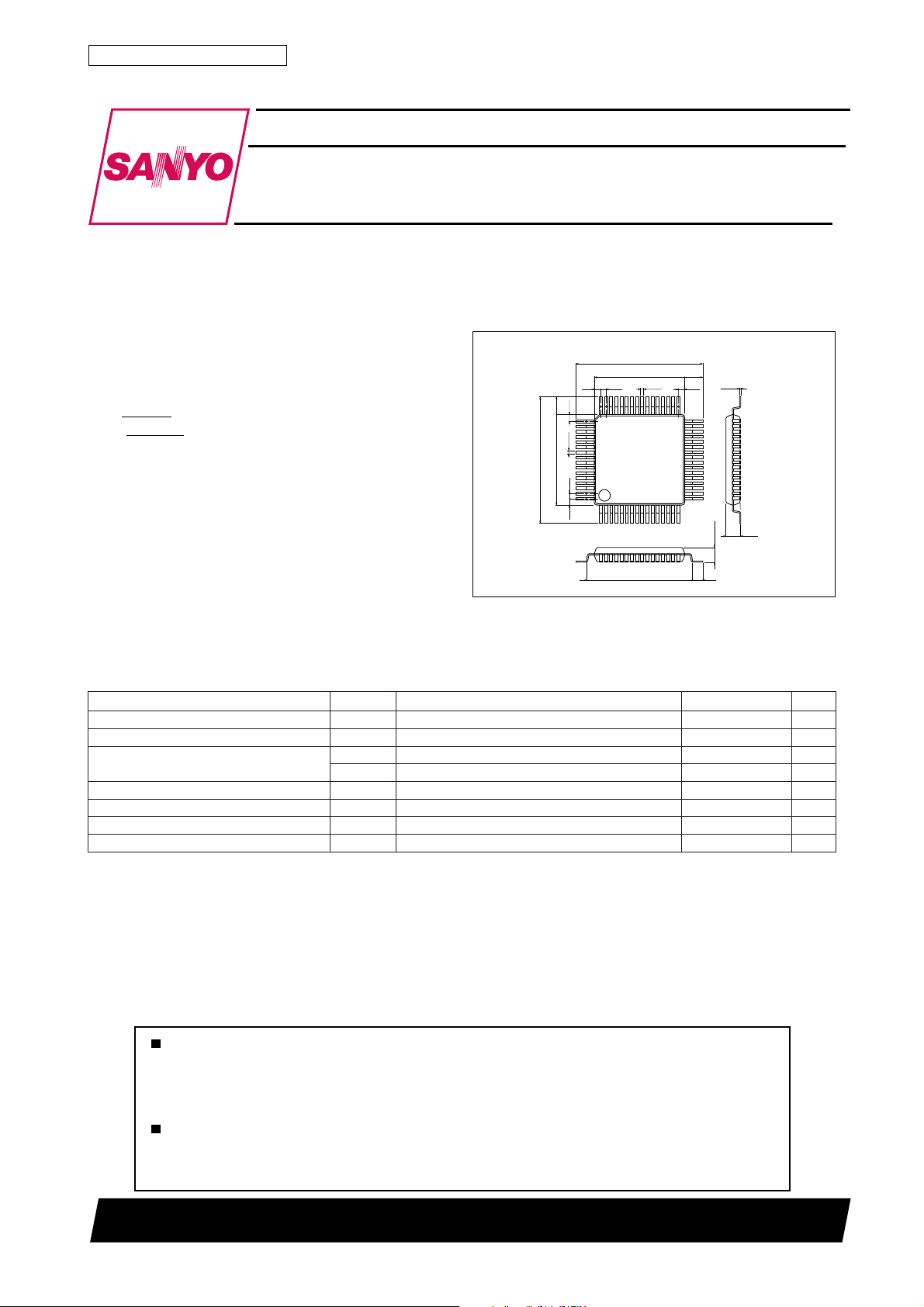
Package Dimensions
unit:mm
3057-QIP64A
[LC7935AN]
20.0
1.0
3.0
1.0
49
0.35
20.0
14.0
0.8
64
1.0
tuptuo–Vot3.0
tuptuorep,tuptuo23Dot1D 03Am
14.0
0.8
48
116
16.6
3.0
1.0
0.35
33
–Vot3.0
0.15
32
17
2.15
2.45max
1.7
SANYO : QIP64A
–0.7+ot3.0V
3.0+V
DD
3.0+V
DD
˚C
˚C
71901TN (KT)/62695TS/7049TA, TS 8-6023 No.3183–1/5
Page 2
LC7935AN
Allowable Operating Conditions at Ta = –10 to +70˚C
retemaraPlobmySsnoitidnoC
egatlovylppuSV
egatlovtupnilevel-HV
egatlovtupnilevel-LV
ycneuqerfkcolCf
htdiweslupkcolCt
emitllaf/esirkcolCt
emitputesataDt
emitdlohataDt
htdiwesluphctaLt
Electrical Characteristics at Ta = 25˚C
retemaraPlobmySsnoitidnoC
tnerructupnilevel-H
tnerructupnilevel-L
egatlovtuptuolevel-HV
egatlovtuptuolevel-L
tnerrucegakaeletats-FFOtuptuOI
ecnaticapactupnIC
niardtnerrucgnitarepOI
IHI2OEB2127Aµ
VLO1S
VLO2V:23Dot1D
V
DD
HI
LI
KLC
WΦ
,rtf
SD
HD
LW
IHI1S
ILI1S
ILI2EBORTS–27–21Aµ
HO
NI
DD
DD
S
NI
S
NI
KCOLC57sn
KCOLC 002sn
S
NI
S
NI
HCTAL001sn
NI
NI
S
V:
TUO
V:
TUO
FFO
KCOLC0.5Fp
V
:DDVDD
daol
sgnitaR
nimpytxam
5.45.5V
EBORTS,OEB,HCTAL,KCOLC,V8.0
EBORTS,OEB,HCTAL,KCOLC,V
%05:ytuD:KCOLC 0.5zHM
KCOLC,001sn
KCOLC,05sn
HCTAL,KCOLC, 01Aµ
HCTAL,KCOLC,–01Aµ
I,V5=
DD
DD
V:23Dot1D
=– Am5.0
HO
I,V5=
DD
O
f,V5=
Am5.0=5.0V
LO
I,V5=
Am03=5.0V
LO
V42=02Aµ
KLC
on:stuptuollA,zHM5=
DD
)L(V2.0
SS
nimpytxam
VDD–5.0
V
DD
DD
sgnitaR
5Am
tinU
V
V
tinU
V
Switching Characteristics at Ta = 25˚C
retemaraPlobmySsnoitidnoC
htdiwyaledhctalkcolCt
htdiwyaledkcolchctaLt
t
emityalednoitagaporptuptuolevel-H
emityalednoitagaporptuptuolevel-L
t
t
t
t
t
Driver ON/OFF Truth Table
)Q(ataDhctaLOEBEBORTSrevirD
000 FFO
100 FFO
010 FFO
110 norevirDNO
001 FFO
101 FFO
011 FFO
111 FFO
LC
CL
1
HLP
2
HLP
3S,KCOLC
HLP
1
LHP
2
LHP
3S,KCOLC
LHP
CLFp51=
CLFp51=
CLFp51=
RLk0.1= Ω C,
sgnitaR
nimpytxam
V:HCTAL,KCOLC
V5=001sn
DD
V:HCTAL,KCOLC
V5=0sn
DD
V:23Dot1D,HCTAL
DD
V:EBORTS,OEB
DD
V:
TUO
DD
V:23Dot1D,HCTAL
DD
Fp51=
L
V:
TUO
DD
R:nD,V5=
k0.1= Ω,
L
R:nD,V5=
k0.1= Ω,
L
S,V5=
TUOC:L
V:23Dot1D,EBORTS,OEB
DD
S,V5=
TUOC:L
Fp51=002sn
R:nD,V5=
k0.1= Ω,
L
:nD,V5=
Fp51=002sn
tinU
004sn
003sn
002sn
001sn
No.3183–2/5
Page 3

Equivalent Circuit Block Diagram
LC7935AN
Output Driver Section Equivalent Circuit
Pin Assignment
No.3183–3/5
Page 4

Input Data Timing Chart
Output Data Timing Chart
LC7935AN
No.3183–4/5
Page 5

LC7935AN
Specifications of any and all SANYO products described or contained herein stipulate the performance,
characteristics, and functions of the described products in the independent state, and are not guarantees
of the performance, characteristics, and functions of the described products as mounted in the customer's
products or equipment. To verify symptoms and states that cannot be evaluated in an independent device,
the customer should always evaluate and test devices mounted in the customer's products or equipment.
SANYO Electric Co., Ltd. strives to supply high-quality high-reliability products. However, any and all
semiconductor products fail with some probability. It is possible that these probabilistic failures could
give rise to accidents or events that could endanger human lives, that could give rise to smoke or fire,
or that could cause damage to other property. When designing equipment, adopt safety measures so
that these kinds of accidents or events cannot occur. Such measures include but are not limited to protective
circuits and error prevention circuits for safe design, redundant design, and structural design.
In the event that any or all SANYO products(including technical data,services) described or
contained herein are controlled under any of applicable local export control laws and regulations,
such products must not be exported without obtaining the export license from the authorities
concerned in accordance with the above law.
No part of this publication may be reproduced or transmitted in any form or by any means, electronic or
mechanical, including photocopying and recording, or any information storage or retrieval system,
or otherwise, without the prior written permission of SANYO Electric Co. , Ltd.
Any and all information described or contained herein are subject to change without notice due to
product/technology improvement, etc. When designing equipment, refer to the "Delivery Specification"
for the SANYO product that you intend to use.
Information (including circuit diagrams and circuit parameters) herein is for example only ; it is not
guaranteed for volume production. SANYO believes information herein is accurate and reliable, but
no guarantees are made or implied regarding its use or any infringements of intellectual property rights
or other rights of third parties.
This catalog provides information as of July, 2001. Specifications and information herein are subject to
change without notice.
PS No.3183–5/5
 Loading...