

Page 1
Ordering number : EN*5236
22896HA (OT) No. 5236-1/10
Overview
The LC78845Q is a synchronous sample rate converter for
digital audio signals.
Features
• Converts data sampled at 32 or 48 kHz to 44.1-kHz
sampled data.
• Passes 44.1-kHz sampled data trough without change.
• Supports 384fs and 512fs system clock rates.
•8× oversampling filters
• Soft muting function
• Built-in PLL circuit
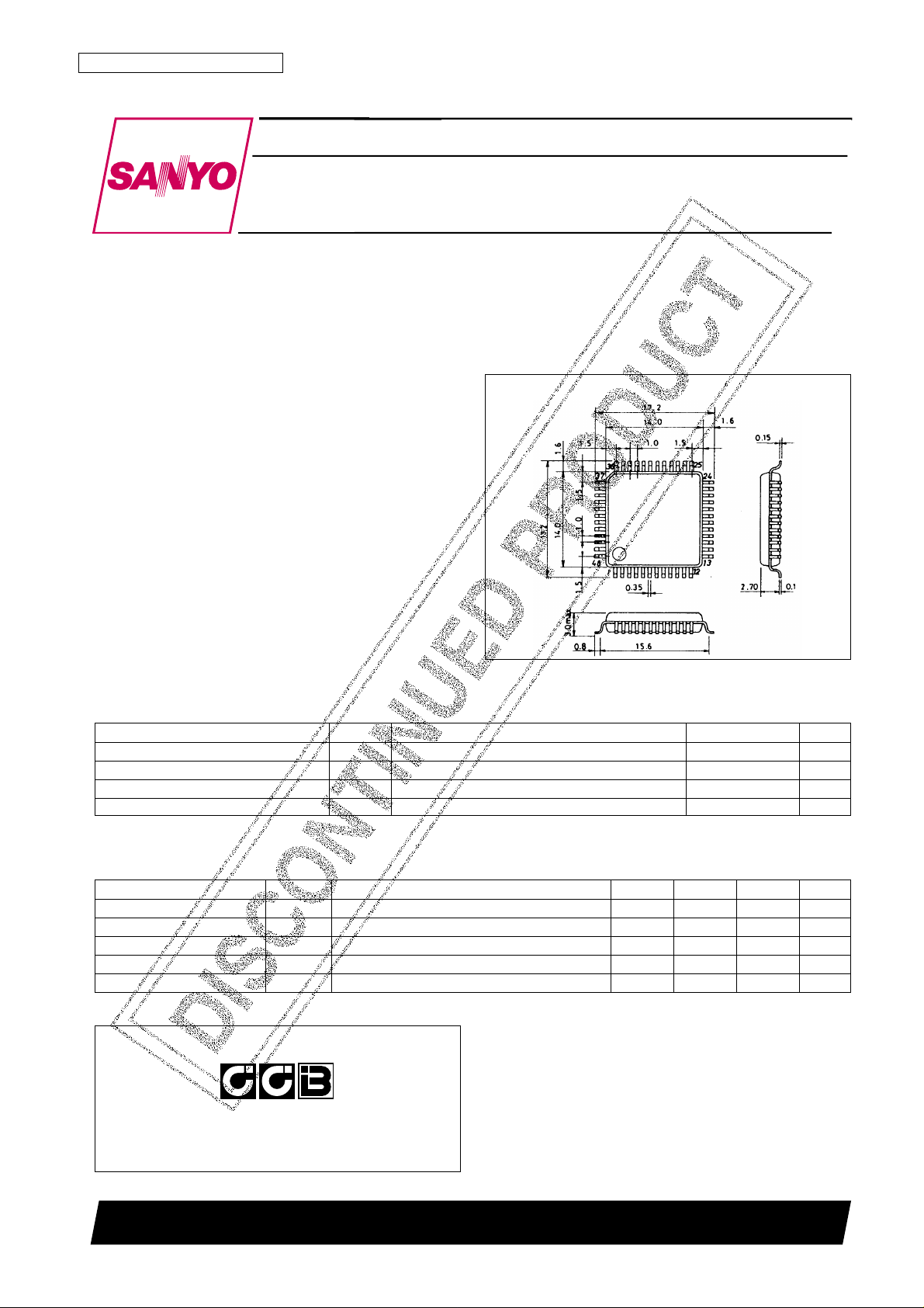
Package Dimensions
unit: mm
3156-QFP48E
Preliminary
SANYO: QIP48E
[LC78845Q]
LC78845Q
SANYO Electric Co.,Ltd. Semiconductor Bussiness Headquarters
TOKYO OFFICE Tokyo Bldg., 1-10, 1 Chome, Ueno, Taito-ku, TOKYO, 110-0005 JAPAN
Sample Rate Converter for Digital Audio
CMOS LSI
This LSI can easily use CCB that is SANYO’s original bus format.
• CCB is a trademark of SANYO ELECTRIC CO., LTD.
• CCB is SANYO’s original bus format and all the bus
addresses are controlled by SANYO.
Specifications
Absolute Maximum Ratings at Ta = 25°C
DC Characteristics
Parameter Symbol Conditions Ratings Unit
Maximum supply voltage V
DD
max –0.3 to +7.0 V
I/O voltages V
I
, V
O
–0.3 to VDD+ 0.3 V
Operating temperature Topr –30 to +70 °C
Storage temperature Tstg –55 to +125 °C
Parameter Symbol Conditions min typ max Unit
Input voltage range V
IN
Ta = –30 to +70°C 0 V
DD
V
Input high-level voltage V
IH
0.7 V
DD
V
Input low-level voltage V
IL
0.3 V
DD
V
Output high-level voltage V
OHIOH
= –1 µA VDD– 0.05 V
Output low-level voltage V
OL
IOL= 1 µA VSS+ 0.05 V
Page 2
AC Characteristics
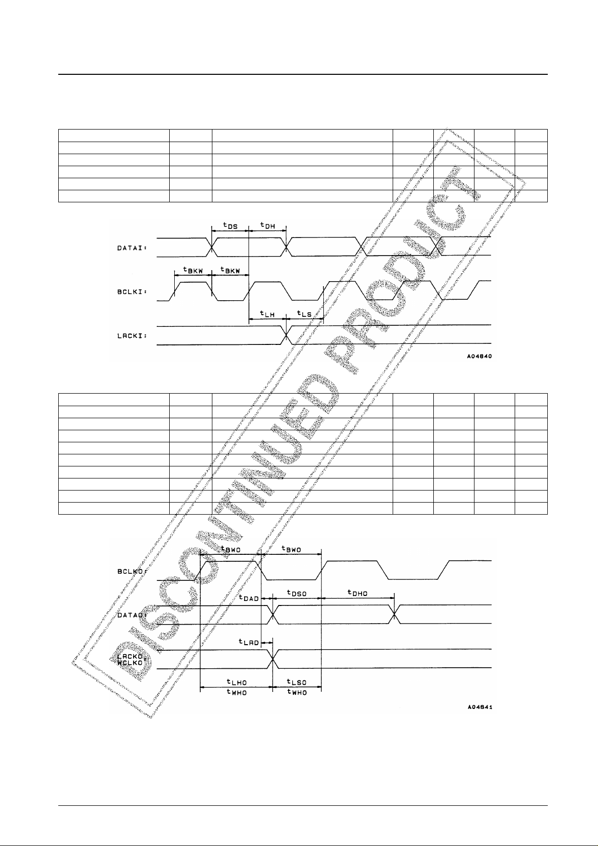
1. Audio data input
2. Audio data output
No. 5236-2/10
LC78845Q
Parameter Symbol Conditions min typ max Unit
BCLKI pulse width t
BKW
50 ns
DATAI setup time t
DS
20 ns
DATAI hold time t
DH
20 ns
LRCKI hold time t
LH
25 ns
LRCKI setup time t
LS
25 ns
Parameter Symbol Conditions min typ max Unit
BCLKO pulse width t
BWO
100 ns
DATAO output delay time t
DAD
25 ns
DATAO setup time t
DSO
50 ns
DATAO hold time t
DHO
50 ns
LRCKO output delay time t
LRD
25 ns
LRCKO setup time t
LSO
50 ns
LRCKO hold time t
LHO
50 ns
WCLKO setup time t
WSO
50 ns
WCLKO hold time t
WHO
50 ns
Page 3
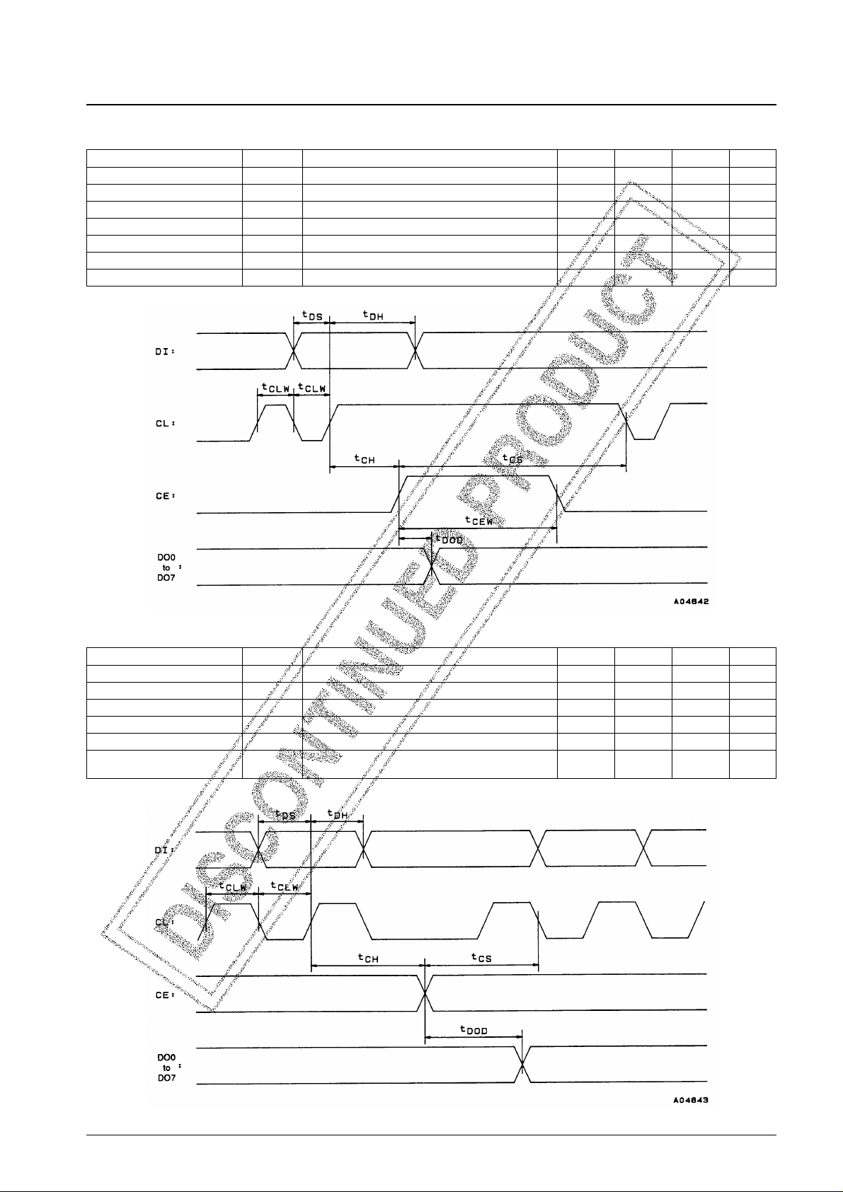
3. Serial input (CCB = low)
4. Serial input (CCB = high)
No. 5236-3/10
LC78845Q
Parameter Symbol Conditions min typ max Unit
CL pulse width t
CLW
50 ns
DI setup time t
DS
20 ns
DI hold time t
DH
20 ns
CE pulse width t
CEW
50 ns
CE setup time t
CS
20 ns
CE hold time t
CH
20 ns
DO0 to DO7 output delay time t
DOD
25 ns
Parameter Symbol Conditions min typ max Unit
CL pulse width t
CLW
50 ns
DI setup time t
DS
20 ns
DI hold time t
DH
20 ns
CE setup time t
CS
20 ns
CE hold time t
CH
20 ns
DO0 to DO7 output delay time
t
DOD
25 ns
with respect to the rise of CE
Page 4

Pin Assignment
Although the DV
DD
and AVDDpins in this IC are given different names to correspond to the internal circuit structure,
they are connected internally through the circuit substrate. As a result, if different voltages are applied to these pins,
abnormal currents will flow in the chip. Since this can cause latchup, power supplies with identical voltages and identical
power-on timings must be used.
Pin Functions
No. 5236-4/10
LC78845Q
Pin No. Symbol Overview Function
1
2
3
4
5
6
7
8
9
10
11
MKSEL
INITB
MCK1
BCLKI
DGND
DGND
DV
DD
LRCKI
DATAI
CCB
SPSEL
DF master clock selection
Reset input
DF master clock input
Audio signal input
Digital system ground
Digital system ground
Digital system power supply
Audio signal input
Serial input format specification
Serial/parallel control
Low: 384fs, high: 512fs
Low: initialization operation
Audio signal bit clock input pin
Audio signal left/right clock and data input pins
Selects the input format for data from the microprocessor input pins.
Allows certain of the setting pins to be set from serial data over the
microprocessor interface.
Low: serial, high: parallel (states set by input pins)
Continued on next page.
Page 5

Continued from preceding page.
No. 5236-5/10
LC78845Q
Pin No. Symbol Overview Function
12
13
14
15
16
17
18
19
20
21
22
23
24
25
26
27
28
29
30
31
32
33
34
35
36
37
38
39
40
41
42
43
44
45
46
47
48
CE
CL
DI
DO7
DO6
DO5
DGND
DV
DD
DO4
DO3
DO2
DO1
DO0
DATAO
LRCKO
WCLKO
BCLKO
DGND
N.C
AGND
VCO
VIN
R
STOP
UNLK
MCK2
AV
DD
AV
DD
MUTE
FSEL3
TEST1
DV
DD
DV
DD
FSEL2
FSEL1
TEST2
TEST3
Microprocessor input pins
Parallel data output
Digital system ground
Digital system power supply
Parallel data output
Audio signal output
Digital system ground
—
Analog system ground
PLL control
PLL control
PLL control
Oscillator stop signal input
Unlock detection output
Synchronization clock output
Analog system power supply
Analog system power supply
Muting
Output data fs selection
Test pin
Digital system power supply
Digital system power supply
Input signal fs selection
Test pins
Data enable signal input
Shift clock input
Address/data input
Output of 8-bit parallel data according to microprocessor input
Output of 8-bit parallel data according to microprocessor input
Audio signal outputs (data, left/right clock, word clock, and bit clock)
Low-pass filter connection
Free-running setting
VCO band adjustment
Low: oscillator stopped, high: PLL running
Outputs a high level when the PLL circuit is unlocked.
Outputs the clock generated by the VCO.
Low: muting off, high: muting on
Low: fs data, high: 2fs data
Must be held low during normal operation.
Selects the fs for the input signal.
Must be held low during normal operation.
Page 6

Block Diagram
Note: 1. BCLKI, LRCKI, DATAI
2. BCLKO, LRCKO, DATAO, WCLKO
3. R, VIN, VCO, UNLK
4. MKSEL, FSEL1, FSEL2, MUTE, STOP
5. CCB, SPSEL, CE, CL, DI
No. 5236-6/10
LC78845Q
Page 7

Input and Output Formats
1. Input format
Audio data is input through the audio data input pins (BCLKI, LRCKI, and DATAI) in the following format.
MKSEL = L: f
BCK
= 48fs
MKSEL = H: f
BCK
= 64fs
2. Output format 1
Audio data is output through the audio data output pins (BCLKO, WCLKO, LRCKO, and DATAO) in the following
format.
BCLKO = 64fs (fixed)
LRCKO = fs (fixed)
WCLKO = 2fs (fixed)
3. Output format 2 (When the input fs is 44.1 kHz)
When data sampled at 44.1 kHz is input, that data is output directly without change. The WCLKO output is held low
in this case.
No. 5236-7/10
LC78845Q
Page 8

Pin Settings
1. Input master clock setup (when SPSEL is high)
Input the master clock for the internal digital filters to MCK1 (pin 3). Also, set whether that clock is 384fs or 512fs
with MKSEL (pin 1).
2. Input data fs setting (when SPSEL is high)
The input data sampling frequency must be set. FSEL1 and FSEL2 (pins 46 and 45) are used for this setting. Data
sampled at a 32 or 48 kHz sampling frequency is converted to data with a 44.1 kHz sampling frequency. If data
sampled at 44.1 kHz is input, it is passed through unchanged.
3. Output data setup
The output data can be switched between fs and 2fs. FSEL3 (pin 41) is used to change this setting.
4. Setup from serial input
The MKSEL, FSEL1, FSEL2, MUTE, and STOP settings can be set using the serial bus by setting SPSEL (pin 11)
low. The 8 bits of input data is output in parallel regardless of the SPSEL setting.
Serial input format 1 (CCB = high)
Serial input format 2 (CCB = low)
No. 5236-8/10
LC78845Q
Pin L H
MKSEL 384fs 512fs
Sampling frequency FSEL1 FSEL2
44.1 kHz 0
✕
48 kHz 1 0
32 kHz 1 1
Pin L H
FSEL3 fs 2fs
Page 9

The data and the signals correspond as listed in the tables. Since the external pins (MKSEL etc.) set by the serial
input are unused, applications must assure that these pins do not become floating. If initialization is performed, set
the initial values listed in the table.
5. Muting
A soft muting function is applied to the data if the MUTE pin (pin 40) is set high when data with a 32 or 48 kHz
sampling frequency is input. The input signal values are gradually attenuated so that the data reaches –∞ 1024/fs
(seconds) later. When the soft muting function is turned off, the amplitude becomes the same as that of the input
1024/fs (seconds) later.
For input data with a 44.1 sampling frequency, the data is forcibly set to 0 on the next rising edge of the LRCK
signal after the MUTE signal goes from low to high. Similarly, data is output on the next rising edge of the LRCK
signal after the MUTE signal goes from high to low.
6. Initialization
When power is first applied, the LSI must be initialized when the pin settings are changed. Initialization is performed
by holding INITB (pin 2) low for at least 1 µs in the state where the MCK1 signal is input after the power supply
voltage has stabilized.
No. 5236-9/10
LC78845Q
Data
INITB = H
INITB = L
SPSEL = L
B0 to B3 LSI selection —
A0 to A3 Address —
D0 MKSEL L
D1 FSEL1 L
D2 FSEL2 L
D3 MUTE H
D4 STOP L
D5 to D7 — H
Page 10

PS No. 5236-10/10
LC78845Q
7. PLL block
The PLL block generates a 14.112 MHz master clock (MCK2) that is used for all three frequencies; 32, 44.1, and
48 kHz, when either 32 or 48 kHz is specified as the input data sampling frequency.
• STOP pin setting
• UNLK pin
The UNLK pin is high during unlocked periods and during the 1024/fs (seconds) required for the unlocked to locked
transition. The LSI performs the same processing during the locked to unlocked transition as it does when MUTE is
high.
• External circuits
This catalog provides information as of February, 1996. Specifications and information herein are subject to
change without notice.
■ No products described or contained herein are intended for use in surgical implants, life-support systems, aerospace
equipment, nuclear power control systems, vehicles, disaster/crime-prevention equipment and the like, the failure of
which may directly or indirectly cause injury, death or property loss.
■ Anyone purchasing any products described or contained herein for an above-mentioned use shall:
➀ Accept full responsibility and indemnify and defend SANYO ELECTRIC CO., LTD., its affiliates, subsidiaries and
distributors and all their officers and employees, jointly and severally, against any and all claims and litigation and all
damages, cost and expenses associated with such use:
➁ Not impose any responsibility for any fault or negligence which may be cited in any such claim or litigation on
SANYO ELECTRIC CO., LTD., its affiliates, subsidiaries and distributors or any of their officers and employees
jointly or severally.
■ Information (including circuit diagrams and circuit parameters) herein is for example only; it is not guaranteed for
volume production. SANYO believes information herein is accurate and reliable, but no guarantees are made or implied
regarding its use or any infringements of intellectual property rights or other rights of third parties.
STOP Function
L The VCO is stopped.
H The VCO operates.
UNLK Function
L Indicates that the PLL circuit is locked.
H Indicates that the PLL circuit is in the unlocked state.
Symbol Value Unit
R1 150
R2 5.1 k
Ω
R3 5.1 k
R4 24 k
C1 0.02
µF
C2 0.1
 Loading...