

Ordering number : EN4532C432
22898HA(OT)/12395TH(KOTO)/N1093(KOTO) No. 4532-1/10
LC75821E, 75821W
SANYO Electric Co.,Ltd. Semiconductor Bussiness Headquarters
TOKYO OFFICE Tokyo Bldg., 1-10, 1 Chome, Ueno, Taito-ku, TOKYO, 110-0005 JAPAN
LCD Display Drivers
CMOS LSI
Overview
The LC75821E and LC75821W are general-purpose LCD
display drivers that can be used for frequency display in
microprocessor-controlled radio receivers and in other
display applications.
Features
• 53 segment outputs (the maximum for static drive)
• Two drive types: static (1/1) duty (53 segments) and 1/2
duty (104 segments)
• Data input: 3 serial input pins
• INH pin for turning off all display output
• The difference form the LC7582: The LC75821E,
LC75821W are A/D converter, DSP function-removed
versions of the LC7582 of which the functions other
than the two can be used with pin compatibility with
the LC7582 kept.
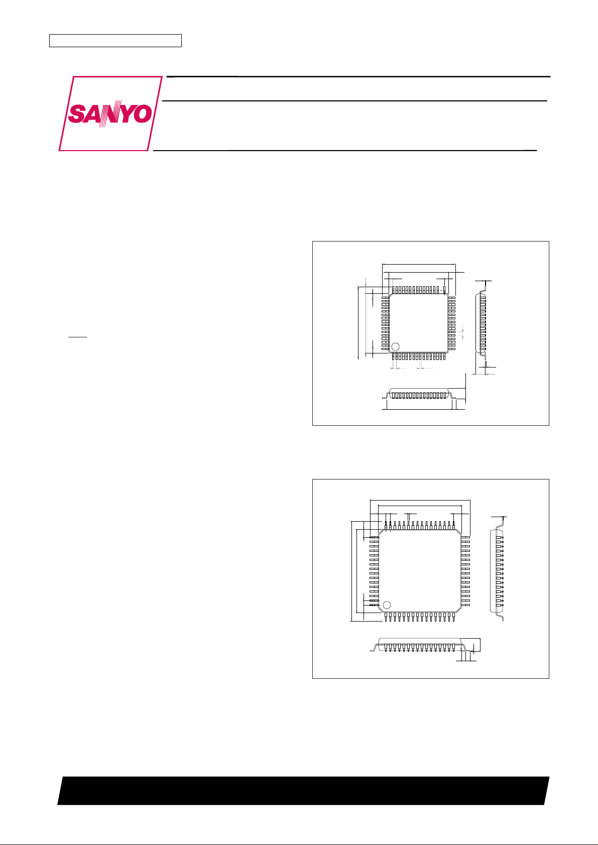
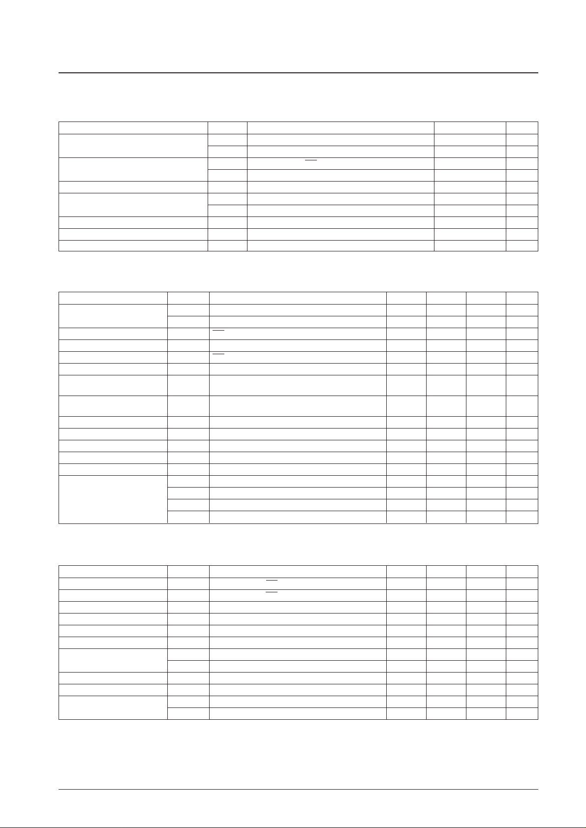
Package Dimensions
unit: mm
3159-QFP64E
unit: mm
3190-SQFP64
1
16
17
32
33
48
49
64
1.0
14.0
17.2
1.0
1.0
1.6
0.15
0.35
0.1
15.6
0.8
0.8
3.0max
2.7
14.0
17.2
1.0
1.6
0.8
SANYO: QIP64E
[LC75821E]
10.0
12.0
1.25
0.5
1.25
1.25
0.5
1.25
0.18
12.0
10.0
0.5
1.7max
0.5
0.1
0.15
116
17
32
33
48
49
64
SANYO: SQFP64
[LC75821W]
Specifications
Absolute Maximum Ratings at Ta = 25°C, VSS= 0 V
Allowable Operating Ranges at Ta = –40 to +85°C, VSS= 0 V
Electrical Characteristics for the Allowable Operating Ranges
No. 4532-2/10
LC75821E, 75821W
Parameter Symbol Conditions Ratings Unit
Maximum supply voltage
V
DD
max V
DD
–0.3 to +7.0 V
V
LCD
V
LCD
–0.3 to VDD+ 0.3 V
Input voltage
V
IN
1 CE, CLK, DATA, INH –0.3 to +7.0 V
V
IN
2 OSC: output off –0.3 to VDD+ 0.3 V
Output voltage V
OUT
OSC: output off –0.3 to VDD+ 0.3 V
Output current
I
OUT
1 S1 to S53 100 µA
I
OUT
2 COM1, COM2 1.0 mA
Allowable power dissipation Pd max Ta = 85°C 100 mW
Operating temperature Topr –40 to +85 °C
Storage temperature Tstg –55 to +125 °C
Parameter Symbol Conditions min typ max Unit
Supply voltage
V
DD
V
DD
3.0 6.5 V
V
LCD
V
LCD
3.0 V
DD
V
Input high-level voltage V
IH
1 INH 0.7 V
DD
6.5 V
Input high-level voltage V
IH
2 CE, CLK, DATA 0.8 V
DD
6.5 V
Input low-level voltage V
IL
1 INH 0 0.3 V
DD
V
Input low-level voltage V
IL
2 CE, CLK, DATA 0 0.2 V
DD
V
Recommended external
R
OSC
OSC 51 kΩ
resistance
Recommended external
C
OSC
OSC 680 pF
capacitance
Guaranteed oscillation range f
OSC
OSC 25 50 100 kHz
Clock low-level pulse width t
øL
CLK 0.25 µs
Clock high-level pulse width t
øH
CLK 0.25 µs
Data setup time t
sup
CLK, DATA 0.25 µs
Data hold time t
dh
CLK, DATA 0.25 µs
t
1
CE, DATA 1 µs
Serial data pulse width
t
2
CE, CLK 1.25 µs
t
3
1 µs
t
4
4 µs
Parameter Symbol Conditions min typ max Unit
Input high-level current I
IH
CE, CLK, DATA, INH: VI= 6.5 V 5 µA
Input low-level current I
IL
CE, CLK, DATA, INH: VI= 0 V –5 µA
Output high-level voltage V
OH
1 S1 to S53: IO= –10 µA VDD– 1.0 V
Output high-level voltage V
OH
2 COM1, COM2: IO= –100 µA V
LCD
– 0.6 V
Output low-level voltage V
OL
1 S1 to S53: IO= 10 µA 1.0 V
Output low-level voltage V
OL
2 COM1, COM2: IO= 100 µA 0.6 V
Mid-level voltage
V
MID
1 COM1, COM2: V
LCD
= 6.5 V, IO= ±100 µA 2.65 3.25 3.85 V
V
MID
2 COM1, COM2: V
LCD
= 3.0 V, IO= ±100 µA 0.9 1.5 2.1 V
Oscillator frequency f
OSC
OSC: R = 51 kΩ, C = 680 pF 40 50 60 kHz
Hysteresis voltage V
H
CE, CLK, DATA: VDD= 5 V 0.3 V
Current drain
I
DD
0.6 mA
I
LCD
V
LCD
2 mA

Pin Assignment
Block Diagram
Pin Functions
No. 4532-3/10
LC75821E, 75821W
Pin Function
S1 to S53 Segment output pins
COM1, COM2 Common output pins (Only COM1 is used in static (1/1) drive. COM2 must be left open in that mode.)
V
LCD
LCD bias voltage setting
OSC Oscillator connection
CE, CLK, DATA Serial data transfer inputs
V
SS
, V
DD
Power supply
Display off control input
INH
INH = low (VSS) ..........Display off (S1 to S53, COM1, COM2 = low)
INH = high (V
DD
).........Display on
Note that serial data transfers can be performed when display output is forced off.
OPEN Make no connections to this pin.

Data Transfer Format
1. Static (1/1) duty
2. 1/2 duty (Only 56 bits need to be transferred if there are no more than 52 display segments. The transfer format is
identical to the static duty case. It is not possible to change the D54 to D106 data without specifying the D1 to D53
data.)
D1 to D53: Display data (1/1 duty) Lighted at 1
D1 to D106: Display data (1/2 duty) Unlighted at 0
DP: Drive type selection bit
1/2 duty at 1
1/1 duty at 0
×: don’t care
Data Transfer Examples
1. Static duty
2. 1/2 duty with 52 or fewer segments
3. 1/2 duty with more than 52 segments
Note: The following transfer format is not allowed in 1/2 duty with 52 or fewer segments.
No. 4532-4/10
LC75821E, 75821W
Transfer direction (56 bits)
Transfer direction (112 bits)
The values of bits D53 and D106 are ignored.(don’t care)

Serial Data
1. Static duty (56 bits)
2. 1/2 duty (112 bits)
Output Waveforms
1. Static duty
No. 4532-5/10
LC75821E, 75821W
Internal latch 1
Internal latch 1
Internal latch 2
Segment off period
Segment on period

2. 1/2 duty
Display Examples
1. Static drive (1/1 duty)
2. 1/2 duty drive
No. 4532-6/10
LC75821E, 75821W
S1 to S52 outputs when the
COM1 segment is on
S1 to S52 outputs when the
COM2 segment is on
S1 to S52 outputs when
both the COM1 and COM2
segments are on
S1 to S52 outputs when
both the COM1 and COM2
segments are off
Example with 40 segments (Up to 53 segments can be driven.)
Note: Numbers in circles indicate the number of segments used.
Example with 80 segments (Up to 104 segments can be driven.)

Sample Application Circuit 1
Sample Application Circuit 2
Note: The internal display data is undefined when power (VDD) is first applied. Since a meaningless pattern will be
displayed if the display is turned on in that state, the display should be turned off by setting INH low and turned
on only after display data has been sent from the controller.
No. 4532-7/10
LC75821E, 75821W
From the controller
From the controller

Transfer (external input) Data/Output Pin Correspondence
Note: Only COM1 is used in static (1/1 duty) drive.
No. 4532-8/10
LC75821E, 75821W
DP 0 1
COM1 COM2
Output pin 1/1 duty 1/2 duty
S1 D1
D1
●●
D2 ●●
S2 D2
D3
●●
D4 ●●
S3 D3
D5
●●
D6 ●●
S26 D26
D51
●●
D52 ●●
S27 D27
D54
●●
D55 ●●
S28 D28
D56
●●
D57 ●●
S43 D43
D86
●●
D87 ●●
S44 D44
D88
●●
D89 ●●
S45 D45
D90
●●
D91 ●●
S46 D46
D92
●●
D93 ●●
S47 D47
D94
●●
D95 ●●
S48 D48
D96
●●
D97 ●●
S49 D49
D98
●●
D99 ●●
S50 D50
D100
●●
D101 ●●
S51 D51
D102
●●
D103 ●●
S52 D52
D104
●●
D105 ●●
S53 D53
Always on
●●
Always on ●●

No. 4532-9/10
LC75821E, 75821W
Oscillator Frequency
Refer to the figure below when determining the oscillator frequency.
Figure 1 LC75821E, 75821W Oscillator Frequency vs. CR Constant
Figure 2 LC75821E, 75821W Oscillator Frequency vs. V
DD
Recommended range for external resistance: 10 to 100 kΩ(Carbon resistance)
Recommended range for external capacitance: 330 to 3300 pF
330 to 820 pF: (Ceramic capacitance with a zero temperature coefficient)
1000 to 3300 pF: (Mylar capacitance with a positive temperature
coefficient)
Oscillator frequency, f
OSC
– kHz
Resistance × capacitance value, CR × 10–5(s)
Power supply voltage, VDD– V
Oscillator frequency, f
OSC
– kHz
Ambient temperature, Ta – °C
Oscillator frequency, f
OSC
– kHz

LC75821E, 75821W
PS No. 4532-10/10
This catalog provides information as of February, 1998. Specifications and information herein are subject to
change without notice.
■ No products described or contained herein are intended for use in surgical implants, life-support systems, aerospace
equipment, nuclear power control systems, vehicles, disaster/crime-prevention equipment and the like, the failure of
which may directly or indirectly cause injury, death or property loss.
■ Anyone purchasing any products described or contained herein for an above-mentioned use shall:
➀ Accept full responsibility and indemnify and defend SANYO ELECTRIC CO., LTD., its affiliates, subsidiaries and
distributors and all their officers and employees, jointly and severally, against any and all claims and litigation and all
damages, cost and expenses associated with such use:
➁ Not impose any responsibility for any fault or negligence which may be cited in any such claim or litigation on
SANYO ELECTRIC CO., LTD., its affiliates, subsidiaries and distributors or any of their officers and employees
jointly or severally.
■ Information (including circuit diagrams and circuit parameters) herein is for example only; it is not guaranteed for
volume production. SANYO believes information herein is accurate and reliable, but no guarantees are made or implied
regarding its use or any infringements of intellectual property rights or other rights of third parties.
 Loading...