

Page 1
Overview
The LC75396NE is an electronic volume control system
providing control over volume, balance, 5-band equalizer,
and input switching based on serial inputs.
Functions
• Volume control:
The chip provides 81 levels of volume attenuation: in 1dB step between 0 dB and –79 dB and –∞.
Independent control over left front/rear and right
front/rear channels provides balance control.
• Equalizer:
The chip provides control in 2-dB steps over the range
between +10 dB and –10 dB. Four of the five bands
have peaking equalization; the remaining one, shelving
equalization.
• Selector:
The left and right channels each offer a choice of five
inputs. The L5 and R5 inputs can be turned on and off
independently. An external constant determines the
amplification for the input signal.
• Serial data input
— Supports CCB* format communication with the
system controller.
Features
• Built-in buffer amplifiers reduce the number of external
parts required.
• Silicon gate CMOS process reduces the noise of built-in
switch.
•V
DD
/2 reference voltage generation circuit built in.
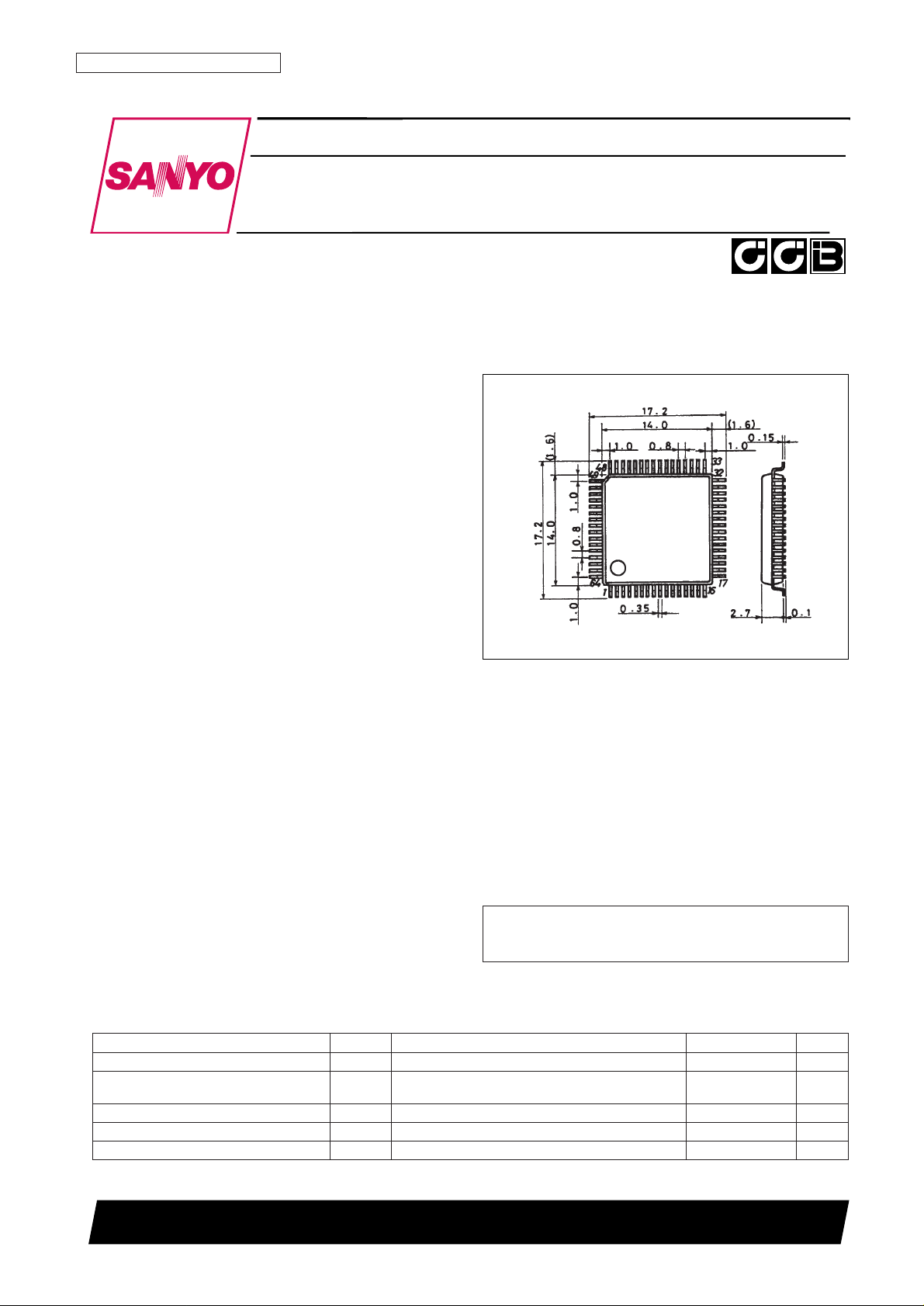
Package Dimensions
unit: mm
3159-QFP64E
CMOS IC
50698RM (OT) No. 5914-1/19
SANYO: QFP64E
[LC75396NE]
SANYO Electric Co.,Ltd. Semiconductor Bussiness Headquarters
TOKYO OFFICE Tokyo Bldg., 1-10, 1 Chome, Ueno, Taito-ku, TOKYO, 110-8534 JAPAN
Single-Chip Electronic Volume Control System
LC75396NE
Ordering number : EN5914
• CCB is a trademark of SANYO ELECTRIC CO., LTD.
• CCB is SANYO’s original bus format and all the bus
addresses are controlled by SANYO.
Parameter Symbol Conditions Ratings Unit
Maximum supply voltage V
DD
max V
DD
11 V
Maximum input voltage V
IN
max
CL, DI, CE, L1 to L5, R1 to R5, LTIN, RTIN, LFIN, RFIN, V
SS
– 0.3 to
V
LRIN, RRIN V
DD
+ 0.3
Allowable power dissipation Pd max Ta ≤ 75°C, with PC board 550 mW
Operating temperature Topr –30 to +75 °C
Storage temperature Tstg –40 to +125 °C
Specifications
Absolute Maximum Ratings at Ta = 25°C, VSS= 0 V
Page 2

No. 5914-2/19
LC75396NE
Parameter Symbol Conditions
Ratings
Unit
min typ max
Supply voltage V
DD
V
DD
6.0 10.5 V
Input high level voltage V
IH
CL, DI, CE 4.0 V
DD
V
Input low level voltage V
IL
CL, DI, CE V
SS
1.0 V
Input voltage amplitude V
IN
CL, DI, CE, L1 to L5, R1 to R5, LTIN, RTIN,
V
SS
V
DD
Vp-p
LFIN, RFIN, LRIN, RRIN
Input pulse width t
øW
CL 1.0 µs
Setup time t
SETUP
CL, DI, CE 1.0 µs
Hold time t
HOLD
CL, DI, CE 1.0 µs
Operating frequency fopg CL 500 kHz
Allowable Operating Ranges at Ta = – 30 to + 75°C, VSS= 0 V
Parameter Symbol Conditions
Ratings
Unit
min typ max
[Input block]
Input resistance Rin L1 to L5, R1 to R5 50 kΩ
Clipping level Vcl LSELO, RSELO: THD = 1.0% 3.00 Vrms
Output load resistance R
L
LSELO, RSELO 10 kΩ
[Volume control block]
Input resistance Rin LFIN, LRIN, RFIN, RRIN 100 kΩ
[Equalizer control block]
Control range Geq Max, boost/cut ±8 ±10 ±12 dB
Step resolution Estep 1 2 3 dB
Internal feedback resistance Rfeed 17 28 39 kΩ
[Overall characteristics]
Total harmonic distortion THD V
IN
= 1 Vrms, f = 1 kHz, with all controls flat overall 0.01 %
Crosstalk CT
V
IN
= 1 Vrms, f = 1 kHz, with all controls flat overall,
80 dB
Rg = 1 kΩ
Output noise voltage
VN1 With all controls flat overall, BW = 20 to 20kHz 2.9 µV
V
N
2
GEQ F1 Band = +10dB, With all controls overall, BW = 20 to 20kHz
17 µV
Output at maximum attenuation V
O
min VIN= 1 Vrms, f = 1 kHz, main volume –∞ –90 dB
Current drain I
DD
VDD– VSS= 10.5 V 46.5 55.8 mA
Input high level current I
IH
CL, DI, CE, VIN= 10.5 V 10 µA
Input low level current I
IL
CL, DI, CE, VIN= 0 V –10 µA
Electrical Characteristics at Ta = 25°C, VDD= 10 V, VSS= 0 V
Page 3
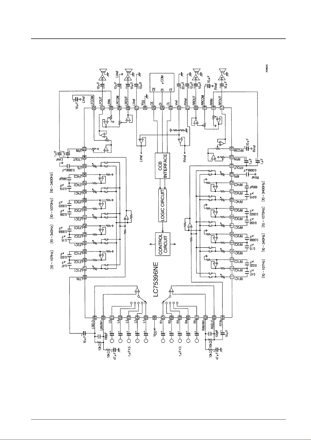
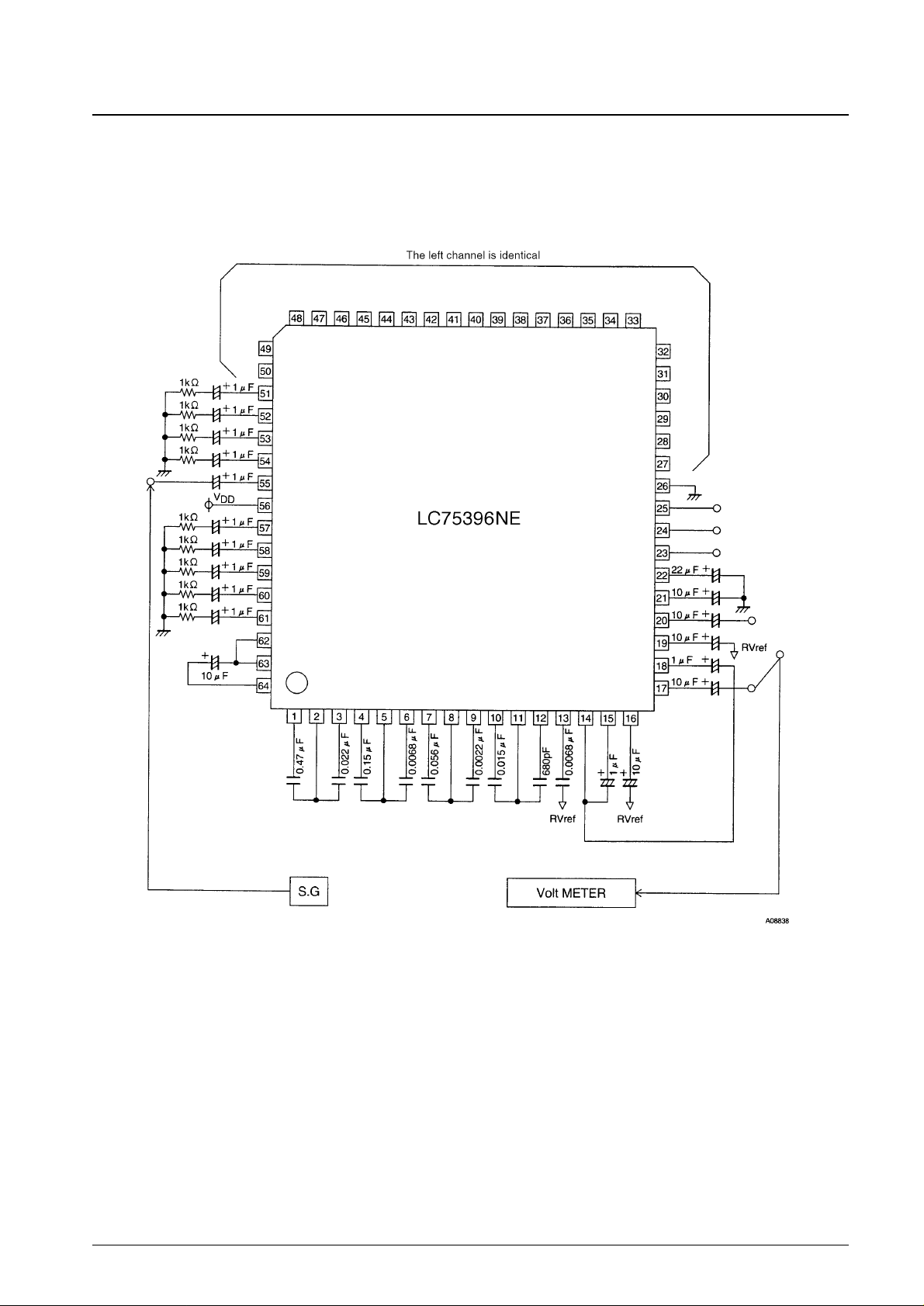
Sample Application Circuit
No. 5914-3/19
LC75396NE
Page 4
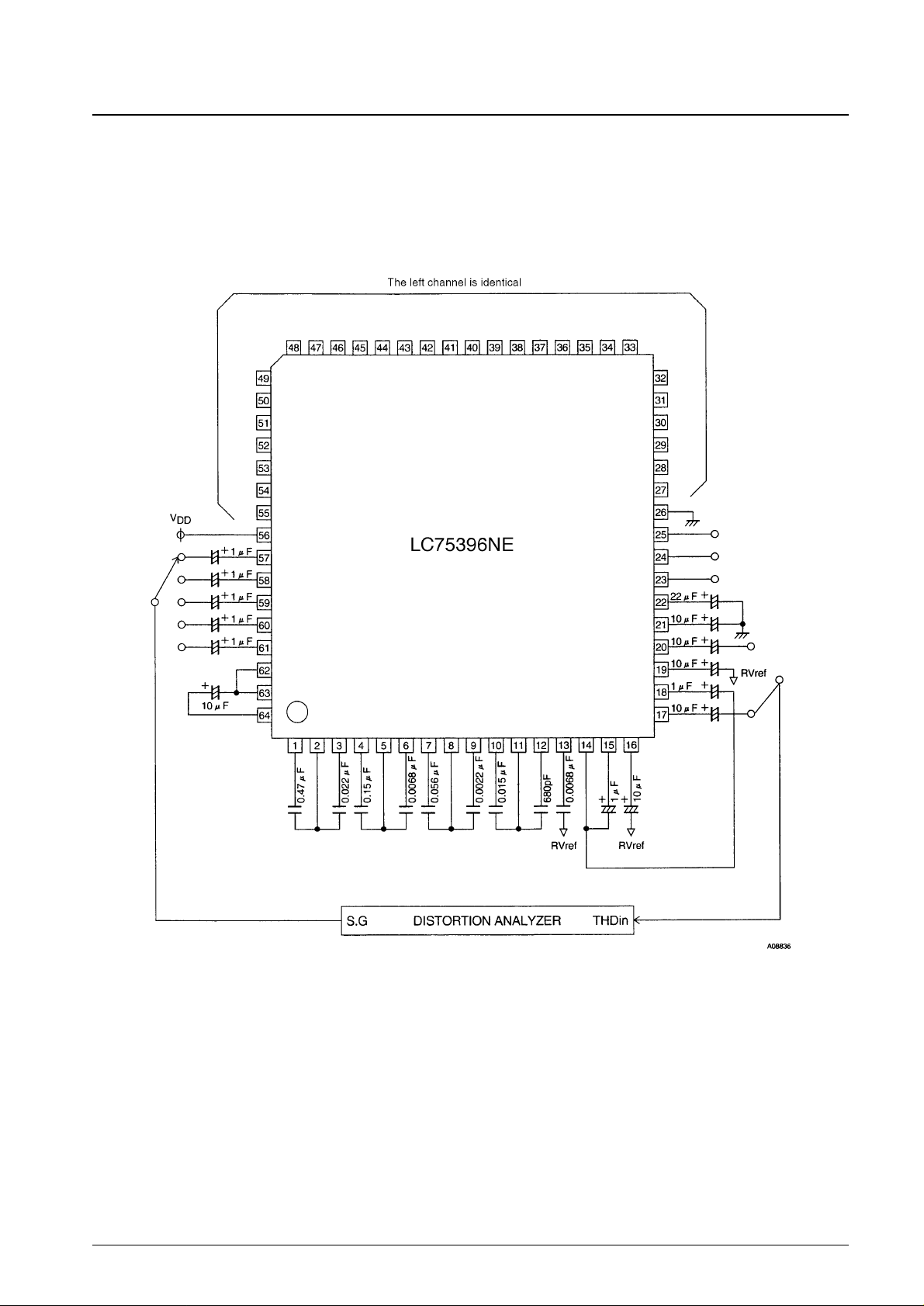
Test Circuits
Total Harmonic Distortion
No. 5914-4/19
LC75396NE
Page 5
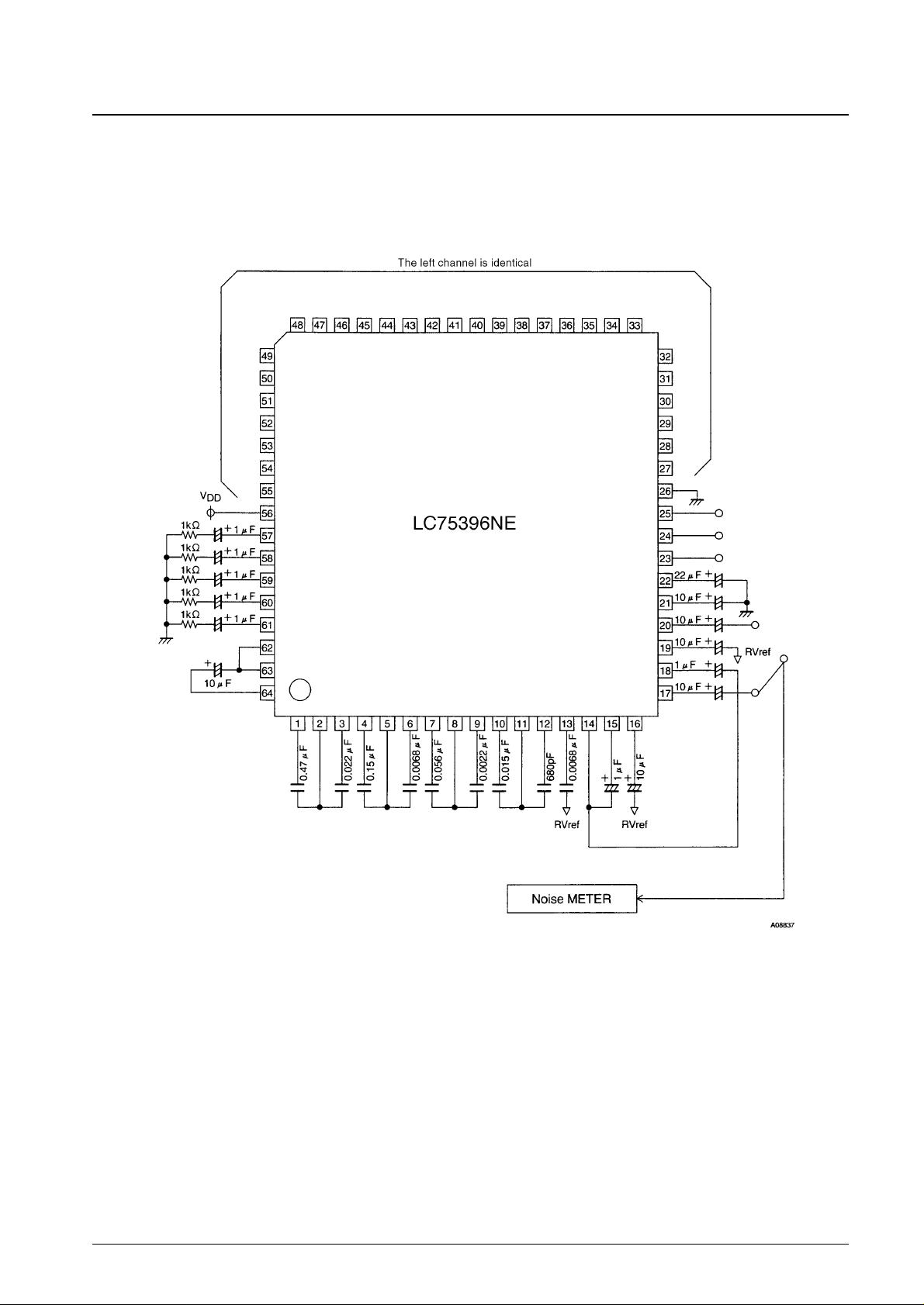
Output Noise Voltage
No. 5914-5/19
LC75396NE
Page 6
Crosstalk
No. 5914-6/19
LC75396NE
Page 7

Pin Assignment
No. 5914-7/19
LC75396NE
Page 8

No. 5914-8/19
LC75396NE
Pin Functions
Pin No. Pin Function Equivalent circuit
Signal inputs
55
54
53
52
51
57
58
59
60
61
L1
L2
L3
L4
L5
R1
R2
R3
R4
R5
Inverting inputs to the operational amplifier that sets the input
gain
50
62
LINVIN1
RINVIN1
Input selector outputs
49
63
LSELO
RSELO
Equalizer inputs
48
64
LTIN
RTIN
· Connections for the capacitors that form the equalizer F1
band filters
Capacitors must be connected between:
LF1C1 (RF1C1) and LF1C2 (RF1C2), and between
LF1C2 (RF1C2) and LF1C3 (RF1C3).
47
46
45
1
2
3
LF1C1
LF1C2
LF1C3
RF1C1
RF1C2
RF1C3
· Connections for the capacitors that form the equalizer F2
band filters
Capacitors must be connected between:
LF2C1 (RF2C1) and LF2C2 (RF2C2), and between
LF2C2 (RF2C2) and LF2C3 (RF2C3).
44
43
42
4
5
6
LF2C1
LF2C2
LF2C3
RF2C1
RF2C2
RF2C3
· Connections for the capacitors that form the equalizer F3
band filters
Capacitors must be connected between:
LF3C1 (RF3C1) and LF3C2 (RF3C2), and between
LF3C2 (RF3C2) and LF3C3 (RF3C3).
41
40
39
7
8
9
LF3C1
LF3C2
LF3C3
RF3C1
RF3C2
RF3C3
· Connections for the capacitors that form the equalizer F4
band filters
Capacitors must be connected between:
LF4C1 (RF4C1) and LF4C2 (RF4C2), and between
LF4C2 (RF4C2) and LF4C3 (RF4C3).
38
37
36
10
11
12
LF4C1
LF4C2
LF4C3
RF4C1
RF4C2
RF4C3
Continued on next page.
Page 9

No. 5914-9/19
LC75396NE
Continued from preceding page.
Pin No. Pin Function Equivalent circuit
• Connections for the capacitors that form the equalizer F5
band filters
Connections for external capacitors
35
13
LF5
RF5
• Input to the left channel front 4-dB step volume control.
• Input to the left channel rear 4-dB step volume control.
• Input to the right channel front 4-dB step volume control.
• Input to the right channel rear 4-dB step volume control.
33
30
15
18
LFIN
LRIN
RFIN
RRIN
• Left channel front volume control output
• Left channel rear volume control output
• Right channel front volume control output
• Right channel rear volume control output
31
28
17
20
LFOUT
LROUT
RFOUT
RROUT
• Equalizer outputs
34
14
LTOUT
RTOUT
• A capacitor of a few tens of µF must be inserted between
Vref and AV
SS(VSS
) to handle power supply ripple in the
V
DD
/2 voltage generation circuit.
22 Vref
• Internal analog system grounds
27
21
LVref
RVref
• Chip enable
When this pin goes from high to low, data is written to an
internal latch and the analog switches operate. Data
transfers are enabled when this pin is at the high level.
25 CE
• Serial data and clock inputs for chip control.
24
23
DI
CL
• Power supply56
V
DD
• Ground26
V
SS
• Common pin for the left channel front 1-dB step volume control.
• Common pin for the left channel rear 1-dB step volume control.
• Common pin for the right channel front 1-dB step volume control.
• Common pin for the right channel rear 1-dB step volume control.
32
29
16
19
LFCOM
LRCOM
RFCOM
RRCOM
Page 10

Equivalent Circuit Diagram
Selector Control Block
Equalizer Control Block
No. 5914-10/19
LC75396NE
Page 11

Volume Control Block
Calculating the Size of External Capacitors
The LC75396NE supports four bands with peaking characteristics and one band with shelving characteristics
1. Peaking Characteristics (bands F1 to F4)
The external capacitor functions as the structural element of a simulated inductor. The equivalent circuit and the
calculations required to achieve the desired center frequency are shown below.
• Equivalent circuit for the simulated inductor
No. 5914-11/19
LC75396NE
Zo: Impedance at resonance
Page 12

• Calculation example
Specifications: Central frequency, FO= 107 Hz
Q factor at maximum boost, Q
+10 dB
= 0.8
— Calculate QO, the sharpness of the simulated inductance itself.
QO= (R1 + R4)/R1 × Q
+10dB
Note: R4 is from the separately issued internal block diagram.
≠ 4.270
— Calculate C1
C1 = 1/2πFOR1QO≠ 0.536 (µF)
— Calculate C2
C2 = QO/2πFOR2 ≠ 0.021 (µF)
• Sample results
2. Shelving characteristics (Band F5)
Achieving the desired control of 2-dB steps over the range between +10 dB to –10 dB requires choosing a capacitor,
C3, with an impedance of 650 Ω.
Control System Timing and Data Formats
To control the LC75396NE, specified sequences are required to be input through the pins CE, CL, and DI. Each sequence
consists of 48 bits: an 8-bit address followed by 40 bits of data.
No. 5914-12/19
LC75396NE
Central frequency C1 C2
F
O
(Hz) (F) (F)
107 0.536 µ 0.021 µ
340 0.169 µ 6663
P
1070 0.054 µ 2117
P
3400 0.017 µ 666
P
Page 13
1. Address Code (B0 to A3)
This product uses an 8-bit address code, and supports the same specifications as other Sanyo CCB serial bus
products.
Address code (LSB)
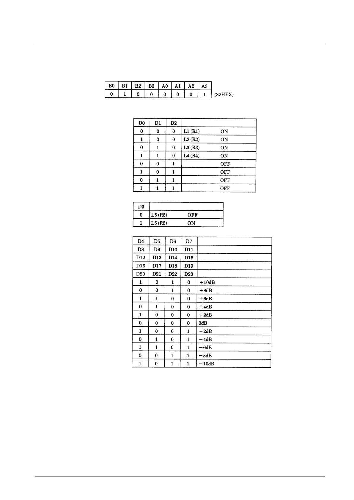
2. Control Code Allocations
Input switching control
Input switching control
Five band equalizer control
No. 5914-13/19
LC75396NE
Operation
Operation
Band f1
Band f2
Band f3
Band f4
Band f5
Page 14

Volume control
Channel selection control
Left channel volume rear/front
control
Right channel volume rear/front
control
Test mode control
Notes: After power is first applied, applications must initialize this chip by sending the initial data (1) and (2) described below.
Initial data ... (1) Address 01000001
Data: (Set the volume to –∞set both D34 and D35 to 1, and set all other data to 0)
(2) Address 01000001
Data: (Set the volume to –∞, set both D34 and D35 to 0, and set all other data to 0)
After transferring that data, set the left and right channel initial settings before turning off the mute function.
No. 5914-14/19
LC75396NE
Initial setting
Rear
Front
Simulataneous left and right
Operation
Operation
Operation
Rear
Front
Operation
These bits are for chip testing and must all be set to 0 in application systems.
Operation
Control is enabled when D33 = 1
Control is enabled when D32 = 1
Page 15

No. 5914-15/19
LC75396NE
fO( Center Frequency) Characteristics
Volume Step Characteristics THD – Frequency Characteristics (1)
Flat overall
When step = –∞
Front and rear volume set to –∞
80-kHz low pass weighting
Gain: 0 dB
Graphic equalizer: flat
Page 16

No. 5914-16/19
LC75396NE
THD – Frequency Characteristics (2)
Total harmonic distortion, THD — %
Total harmonic distortion, THD — %
THD – Frequency Characteristics (3)
Frequency, f — Hz
Volume: 0 dB position
Volume: 0 dB position
Volume: –10 dB position
Volume: –10 dB position
Volume: 0 dB position
All bands boosted
All bands cut
Flat
Volume: –10 dB position
Frequency, f — Hz
THD – Supply Voltage Characteristics (1)
Total harmonic distortion, THD — %
Total harmonic distortion, THD — %
THD – Supply Voltage Characteristics (1)
Supply voltage, VDD— V Supply voltage, VDD— V
80-kHz low pass weighting
Gain: 0 dB
Graphic equalizer: flat
80-kHz low pass weighting
Gain: 0 dB
Volume: 0 dB position
80-kHz low pass weighting
Gain: 0 dB
Graphic equalizer: flat
80-kHz low pass weighting
Gain: 0 dB
Graphic equalizer: flat
Page 17

No. 5914-17/19
LC75396NE
All bands boosted
All bands cut
All bands boosted
All bands cut
Flat
Flat
THD – Supply Voltage Characteristics (3)
Total harmonic distortion, THD — %
Total harmonic distortion, THD — %
THD – Input Level Characteristics (1)
Supply voltage, VDD— V Input level, VIN— dBV
80-kHz low pass weighting
Gain: 0 dB
Volume: 0 dB position
80-kHz low pass weighting
Gain: 0 dB
Volume: 0 dB position
Graphic equalizer: flat
THD – Input Level Characteristics (2)
Total harmonic distortion, THD — %
Total harmonic distortion, THD — %
THD – Input Level Characteristics (3)
Input level, VIN— dBV Input level, VIN— dBV
80-kHz low pass weighting
Gain: 0 dB
Volume: –10 dB position
Graphic equalizer: flat
80-kHz low pass weighting
Gain: 0 dB
Volume: 0 dB position
Page 18

No. 5914-18/19
LC75396NE
Usage Notes
• When the power is first applied, the internal analog switches are in indeterminate states. The chip therefore requires
muting or other external measures until it has received the proper data.
• After power is first applied, applications must initialize this chip by sending the initial data (1) and (2) described below.
Initial data ... (1) Address 01000001
Data: (Set the volume to –∞, set both D34 and D35 to 0, and set all other data to 0)
(2) Address 01000001
Data: (Set the volume to –∞, set both D34 and D35 to 1, and set all other data to 0)
After transferring that data, set the left and right channel initial settings before turning off the mute function.
• Provide grounding patterns or shielding for the lines to the CL, DI, and CE pins so as to prevent their high-frequency
digital signals from interfering with the operation of nearby analog circuits.
All bands boosted
All bands cut
Flat
THD – Output Level Characteristics (1)
Total harmonic distortion, THD — %
Total harmonic distortion, THD — %
THD – Output Level Characteristics (2)
Outut level, VO— dBV Outut level, VO— dBV
80-kHz low pass weighting
Gain: 0 dB
Volume: 0 dB position
Graphic equalizer: flat
THD – Output Level Characteristics (3)
Total harmonic distortion, THD — %
Outut level, VIN— dBV
80-kHz low pass weighting
Gain: 0 dB
Volume: 0 dB position
80-kHz low pass weighting
Gain: 0 dB
Volume: –10 dB position
Graphic equalizer: flat
Page 19

No. 5914-19/19
LC75396NE
This catalog provides information as of May, 1998. Specifications and information herein are subject to change
without notice.
■ No products described or contained herein are intended for use in surgical implants, life-support systems, aerospace
equipment, nuclear power control systems, vehicles, disaster/crime-prevention equipment and the like, the failure of
which may directly or indirectly cause injury, death or property loss.
■ Anyone purchasing any products described or contained herein for an above-mentioned use shall:
➀ Accept full responsibility and indemnify and defend SANYO ELECTRIC CO., LTD., its affiliates, subsidiaries and
distributors and all their officers and employees, jointly and severally, against any and all claims and litigation and all
damages, cost and expenses associated with such use:
➁ Not impose any responsibility for any fault or negligence which may be cited in any such claim or litigation on
SANYO ELECTRIC CO., LTD., its affiliates, subsidiaries and distributors or any of their officers and employees
jointly or severally.
■ Information (including circuit diagrams and circuit parameters) herein is for example only; it is not guaranteed for
volume production. SANYO believes information herein is accurate and reliable, but no guarantees are made or implied
regarding its use or any infringements of intellectual property rights or other rights of third parties.
 Loading...