


CMOS LSI
Ordering number : EN4929A
63096HA (OT)/62095HA (OT) No. 4929-1/11
SANYO Electric Co.,Ltd. Semiconductor Bussiness Headquarters
TOKYO OFFICE Tokyo Bldg., 1-10, 1 Chome, Ueno, Taito-ku, TOKYO, 110 JAPAN
Two-Channel Electronic Volume Control
LC75366, 75366M
Overview
The LC75366 (DIP20) and the LC75366M (MFP20) are
electronic volume controls that can be controlled by serial
input data and provide volume, balance and loudness
functions.
Features
• Silicon gate CMOS process for low switching noise
Functions
• Volume: 0 dB to –68 dB (in 2 dB steps) and –∞;
36 positions.
A balance function can be implemented by controlling
the left and right channel volume settings independently.
• Loudness: Taps are provided at the –20 dB positions in
the 10 dB step resistor ladder used by the volume
control function. A loudness function can be
implemented by attaching external RC circuits at these
tap points.
• An address selection pin (the S pin) allows two
LC75366 chips to be used on the same bus.
• Serial data input: Supports CCB* format communication
with the system controller.
Package Dimensions
unit: mm
3021B-DIP20
• CCB is a trademark of SANYO ELECTRIC CO., LTD.
• CCB is SANYO’s original bus format and all the bus
addresses are controlled by SANYO.
unit: mm
3036B-MFP20
Specifications
Absolute Maximum Ratings at Ta = 25°C, VSS= 0 V
Parameter Symbol Conditions Ratings Unit
Maximum supply voltage V
DD
max V
DD
12 V
Maximum input voltage
V
IN
max1 CL, DI, CE, S VSS– 0.3 to VDD+ 0.3 V
V
IN
max2 L10dBIN, L2dBIN, R10dBIN, R2dBIN VSS– 0.3 to VDD+ 0.3 V
Allowable power dissipation Pd max Ta ≤ 85°C 140 mW
Operating temperature Topr –40 to +85 °C
Storage temperature Tstg –50 to +125 °C
[LC75366]
SANYO: DIP20
SANYO: MFP20
[LC75366M]

Allowable Operating Ranges at Ta = 25°C, VSS= 0 V
Electrical Characteristics at Ta = 25°C, VSS= 0 V
Pin Assignment
No. 4929-2/11
LC75366, 75366M
Parameter Symbol Conditions min typ max Unit
THD (1)
V
IN
= 1 Vrms, f = 1 kHz, all settings flat overall,
0.006 %
Total harmonic distortion
V
DD
= 9 V
THD (2)
V
IN
= 1 Vrms, f = 20 kHz, all settings flat overall,
0.015 %
V
DD
= 9 V
Crosstalk CT
V
IN
= 1 Vrms, f = 20 kHz, all settings flat overall,
85 dB
Rg = 1 kΩ
Output at maximum attenuation V
O
min
V
IN
= 1 Vrms, f = 20 kHz, volume setting: –∞,
–80 dB
with a 470 µF capacitor between L/R Vref and V
SS
Total resistance
R
VOL
(1) 10 dB steps 28.2 47 65.8 kΩ
R
VOL
(2) 2 dB steps 12 20 28 kΩ
L10dBIN, R10dBIN, LCT1, L2dBIN, R2dBIN, RCT1,
Output off leakage current Ioff L10dBOUT, R10dBOUT, LCT2, L2dBOUT, R2dBOUT, –10 +10 µA
RCT2, LVref, RVref
Input high level current I
IH
VI = VDD(CL, CE and DI pins) 10 µA
Input low level current I
IL
VI = VSS(CL, CE and DI pins) –10 µA
Output noise voltage V
N
All settings flat overall (IHF-A), VDD= 9 V, Rg = 1 kΩ 2 10 µV
Current drain I
DD
VDD– VSS= 11 V 1 mA
CT1 180 300 420 Ω
Analog switch on resistance
R
ON
For use between CT2 and Vref 90 150 210 Ω
(Design target value)
0 dB, –∞ 0.6 1.0 1.4 kΩ
Other than the above 6.0 10.0 14.0 kΩ
Parameter Symbol Conditions Ratings Unit
Supply voltage V
DD
V
DD
4.0 to 11.0 V
Input high level voltage
V
IH
(1) CL, DI, CE 0.3 VDD+ 1 to V
DD
V
V
IH
(2) S 0.8 VDDto V
DD
V
Input low level voltage
V
IL
(1) CL, DI, CE VSSto 0.2 V
DD
V
V
IL
(2) S VSSto 0.2 V
DD
V
Input voltage amplitude V
IN
L10dBIN, L2dBIN, R10dBIN, R2dBIN VSSto V
DD
Vp-p
Input pulse width t
øW
CL 1 or longer µs
Setup time t
set up
CL, DI, CE 1 or longer µs
Hold time t
hold
CL, DI, CE 1 or longer µs
Operating frequency fop CL Up to 500 kHz
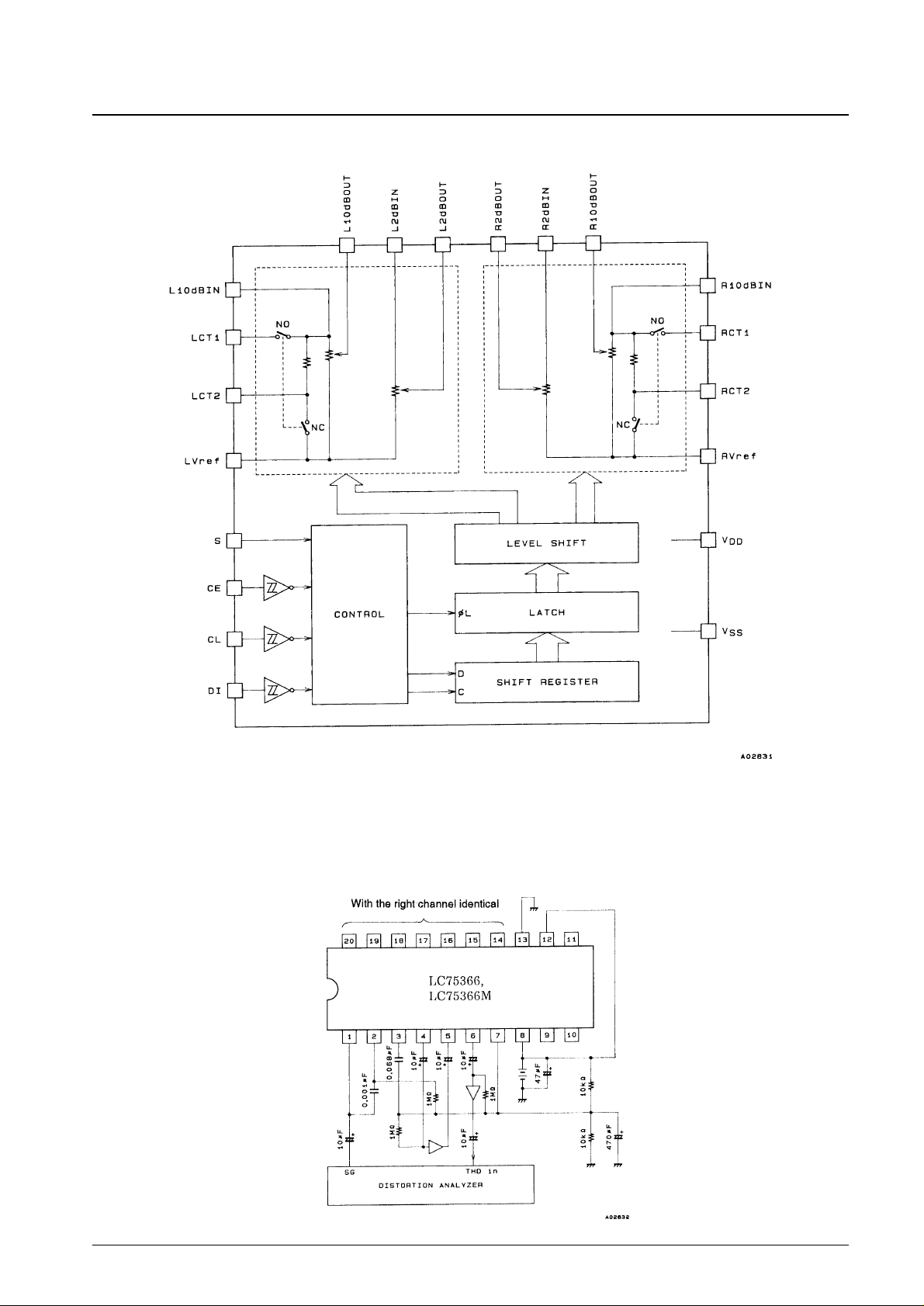
Equivalent Circuit Block Diagram
Test Circuits
1. Total harmonic distortion
No. 4929-3/11
LC75366, 75366M
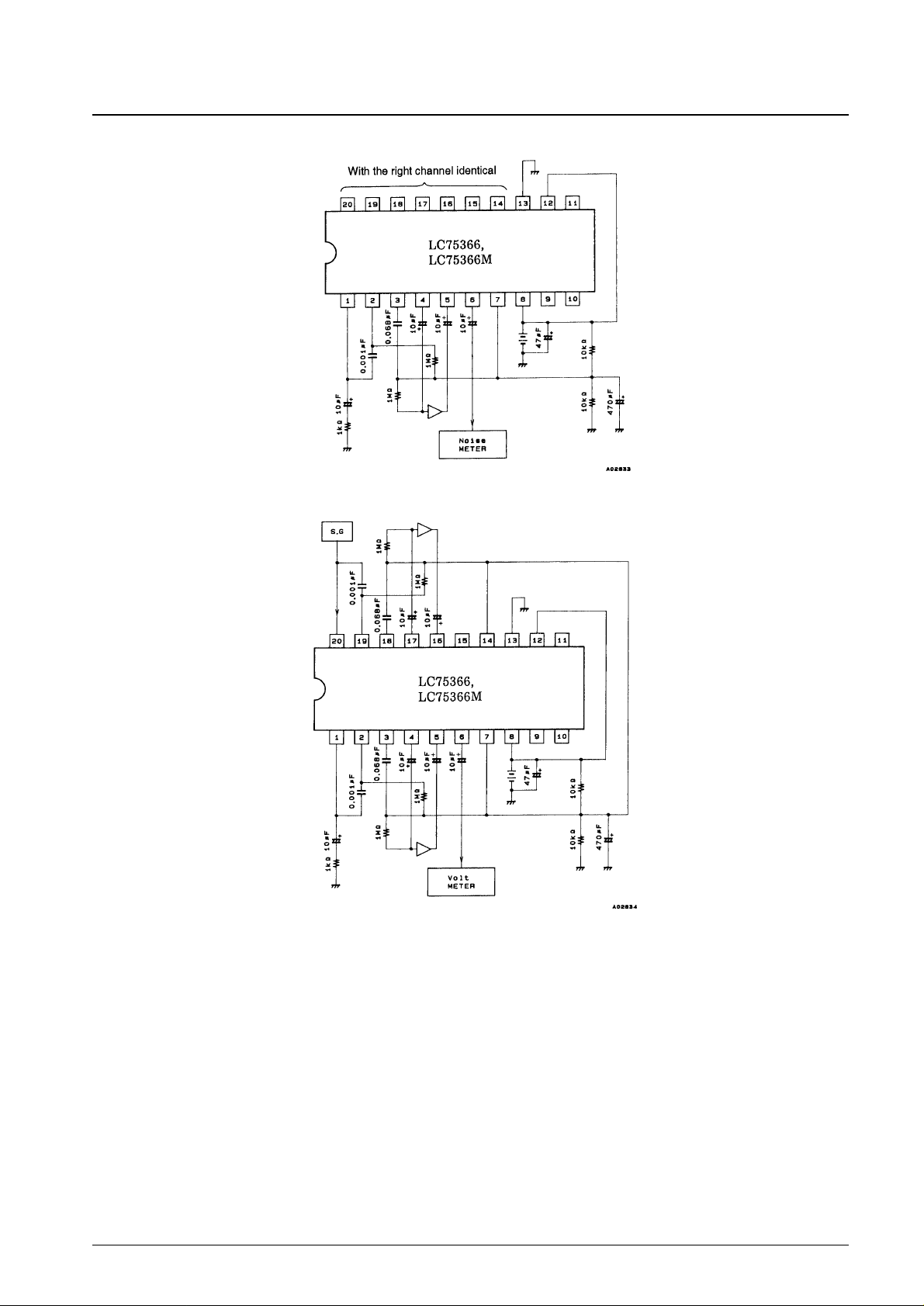
2. Output noise voltage
3. Crosstalk
No. 4929-4/11
LC75366, 75366M

Volume Block Equivalent Circuit
No. 4929-5/11
LC75366, 75366M

Pin Functions
No. 4929-6/11
LC75366, 75366M
Pin No. Symbol Function Note
1
20
2
3
19
18
4
17
5
16
6
15
7
14
12
9
10
11
8
13
L10dBIN
R10dBIN
LCT1
LCT2
RCT1
RCT2
L10dBOUT
R10dBOUT
L2dBIN
R2dBIN
L2dBOUT
R2dBOUT
LVref
RVref
S
CL
DI
CE
V
DD
V
SS
Input pins for the 10 dB step attenuator. Must be driven from a low impedance.
Loudness connections. Connect a high band compensation capacitor between
CT1 and 10dBIN and connect a low band compensation capacitor between CT2
and Vref.
Output pins for the 10 dB step attenuator. These outputs must be received by a
load of about 1 MΩ.
Input pins for the 2 dB step attenuator. Must be driven from a low impedance.
Output pins for the 2 dB step attenuator. These outputs must be received by a
load of about 1 MΩ.
Volume circuit common pins. The impedance of the pattern connected to these
pins should be kept as low as possible.
Since the capacitors between Vref and V
SS
form the residual resistance
components when the volume is cut, adequate care must be taken in
determining the value of these capacitors.
Pin that selects the address code in the data format. Data will be accepted for
an address code of 88 when this pin is tied to V
DD
, and for an address code of
89 when tied to V
SS
.
Serial data and clock inputs for control
Chip enable. The internally latched data is written and the analog switches
operate when this pin goes from high to low. Data transfer is enabled when this
pin is at the high level.
These pins must be connected to the power supply.

Control System Timing and Data Format
Apply the stipulated serial data to the CE, CL and DI pins to control the LC75366 and LC75366M. The data consists of
20 bits, of which 8 bits are the address and 12 bits are control data.
No. 4929-7/11
LC75366, 75366M

Sample Application Circuit
No. 4929-8/11
LC75366, 75366M

No. 4929-9/11
LC75366, 75366M

Loudness Function External Circuit Constant Calculation Example
First, refer to the LC75366 and LC75366M 10 dB step internal equivalent circuit shown on page 5. Figure 1 below
shows this circuit simplified with the external components used for the loudness function connected for this calculation.
The sample calculation below uses this diagram to acquire a 5 dB boost at f = 100 Hz.
(f = 100 Hz, 5 dB boost)
Let R and C in Figure 1 be:
R1 = R2 = 10 kΩ
R3 = 1 kΩ
C1 = Z1, C2 = Z2
Then:
Solving the above equations gives:
Z1 ≠ 178.3 kΩ and Z2 = 176 Ω
No. 4929-10/11
LC75366, 75366M
V
OUT
=
(at = 1 kHz)
+
R2 (R3 + Z2)
R2 + R3 + Z2
= –20 dB
R1 · Z1
R1 + Z1
R2 (R3 + Z2)
R2 + R3 + Z2
V
OUT
=
(at = 100 Hz)
+
= –15 dB
R1 · 10 · Z1
R1 + 10 · Z1
R2 (R3 + 10 · Z2)
R2 + R3 + 10 · Z2
R2 (R3 + 10 · Z2)
R2 + R3 + 10 · Z2

No. 4929-11/11
LC75366, 75366M
Therefore, under such conditions where f = 1 kHz, specifications may be satisfied if C (capacitor) having these
impedances is supplied externally.
The result is that C1 = 893 pF and C2 = 0.9 µF.
Figure 1
Usage Notes
1. The states of the internal analog switches will be indeterminate when power is first applied. Muting should be
applied externally until control data has been transferred and stored.
2. The signal lines for the CL, DI and CE pins should either be covered by the pattern ground or be formed from
shielded cable to prevent the high-frequency digital signals transmitted over these lines from entering the analog
system.
This catalog provides information as of November, 1997. Specifications and information herein are subject to
change without notice.
■ No products described or contained herein are intended for use in surgical implants, life-support systems, aerospace
equipment, nuclear power control systems, vehicles, disaster/crime-prevention equipment and the like, the failure of
which may directly or indirectly cause injury, death or property loss.
■ Anyone purchasing any products described or contained herein for an above-mentioned use shall:
➀ Accept full responsibility and indemnify and defend SANYO ELECTRIC CO., LTD., its affiliates, subsidiaries and
distributors and all their officers and employees, jointly and severally, against any and all claims and litigation and all
damages, cost and expenses associated with such use:
➁ Not impose any responsibility for any fault or negligence which may be cited in any such claim or litigation on
SANYO ELECTRIC CO., LTD., its affiliates, subsidiaries and distributors or any of their officers and employees
jointly or severally.
■ Information (including circuit diagrams and circuit parameters) herein is for example only; it is not guaranteed for
volume production. SANYO believes information herein is accurate and reliable, but no guarantees are made or implied
regarding its use or any infringements of intellectual property rights or other rights of third parties.
 Loading...