

SANYO LC74776, LC74776M Datasheet
Overview
The LC74776/M is an on-screen display controller CMOS
IC that displays characters and patterns on the TV screen
under microprocessor control. This IC includes a built-in
PDC/VPS/UDT interface circuit.
Functions
• Display format: 24 characters by 12 rows (Up to 288
characters)
• Character format: 12 (horizontal) × 18 (vertical) dots
• Character sizes: Three sizes each in the horizontal and
vertical directions
• Characters in font: 256 (Of the 256 characters, one is a
space character (FE hexadecimal)
and one is a transparent space
character (FF hexadecimal))
• Initial display positions: 64 horizontal positions and 64
vertical positions
• Blinking: Specifiable in character units
• Blinking types: Two periods supported:
1.0 second and 0.5 second
• Blanking: Over the whole font (12 × 18 dots)
• Background color: 8 colors (internal synchronization
mode): 4fSCand 2f
SC
Blue background only: NTSC
• Line background color: Three lines can be set up.
8 line background colors (in
internal synchronization mode):
4fSCand 2f
SC
• External control input: 8-bit serial input format
• On-chip sync separator circuit
• Video outputs: PAL and NTSC format composite video
outputs
• On-chip PDC/VPS/UDT interface circuit supporting I2C
• Package: DIP30SD
MFP30S
0.15
15.3
115
30 16
0.651.00.35
2.5max
2.15
0.1
0.65
7.9
9.2
10.5
CMOS IC
Ordering number : EN*6018
20399RM(OT) No. 6018-1/35
Preliminary
SANYO: MFP30S
[LC74776M]
SANYO Electric Co.,Ltd. Semiconductor Bussiness Headquarters
TOKYO OFFICE Tokyo Bldg., 1-10, 1 Chome, Ueno, Taito-ku, TOKYO, 110-8534 JAPAN
On-Screen Display Controller IC
LC74776, 74776M
1
15
30
16
1.14 1.78
27.2
0.25
10.16
8.6
0.48 0.95
3.25
3.0
3.95max
SANYO: DIP30SD
[LC74776]
Package Dimensions
unit: mm
3196-DIP30SD
unit: mm
3216A-MFP30S
Any and all SANYO products described or contained herein do not have specifications that can handle
applications that require extremely high levels of reliability, such as life-support systems, aircraft’s
control systems, or other applications whose failure can be reasonably expected to result in serious
physical and/or material damage. Consult with your SANYO representative nearest you before using
any SANYO products described or contained herein in such applications.
SANYO assumes no responsibility for equipment failures that result from using products at values that
exceed, even momentarily, rated values (such as maximum ratings, operating condition ranges, or other
parameters) listed in products specifications of any and all SANYO products described or contained
herein.
Pin Assignment
No. 6018-2/35
LC74776, 74776M
LC74776
LC74776M
Pin Functions
No. 6018-3/35
LC74776, 74776M
Pin no. Pin Function Notes
1 V
SS
1 Ground Ground connection (digital system ground)
2 Xtal
IN
These pins are used either to connect the crystal and capacitors used to form an external
crystal oscillator circuit to generate the internal synchronizing signals, or to input an external
Xtal
OUT
Crystal oscillator
clock signal (2fsc or 4fsc). As a mask option, the Xtal
OUT
pin can be set to function as
3
(MUTE)
(MUTE input)
the MUTE input pin. When this pin is set low, the video output is held at the pedestal level.
(A pull-up resistor is built in and the input has hysteresis characteristics.)
Switches the mode between external clock input and crystal oscillator operation. A low level
4 CTRL1 selects crystal oscillator operation and a high level selects external clock input. As a mask
(CHABLK) option, the CTRL1 input pin can be set to function as the CHABLK (character . frame)
output. This is a 3-value output.
5 SCL I
2
C clock input Clock input for the PDC/VPS data output. I2C bus.
6 OSC
IN
LC oscillator
Connection for the external coil and capacitor for the oscillator used to generate
connections
the character output dot clock
7 OSC
OUT
Outputs the state of the external synchronizing signal presence/absence judgment. Outputs
External synchronizing
a high level when synchronizing signals are present.
8 SYNC
JDC
signal judgment output
Outputs either the crystal oscillator clock if CS and RST are low, or the VCO clock if CS
and RST are high.
(This signal is not output after a command reset.)
Enable input for the OSD serial data input.
9 CS Enable input Serial data input is enabled when this pin is low.
A pull-up resistor is built in and the input has hysteresis characteristics.
10 SCLK Clock input
Serial data input enable pin.
A pull-up resistor is built in and the input has hysteresis characteristics.
11 SIN Data input
Serial data input.
A pull-up resistor is built in and the input has hysteresis characteristics.
12 V
DD
2 Power supply Composite video signal level adjustment power supply (analog system power supply)
13 CP
OUT
Charge pump output Charge pump output. Connect a low-pass filter to this pin.
14 VCO
IN
Oscillator control voltage input
VCO oscillator control voltage input. (For data slicing)
15 V
SS
3 Ground Ground (VCO ground)
16 VCO
R
Oscillator range adjustment VCO oscillator range adjustment resistor connection
17 NC This pin must either be connected to ground or left open
18 V
DD
3 Power supply (+5 V) Power supply (+5 V: VCO power supply)
19 CV
OUT
Video signal output Composite video signal output
20 V
SS
2 Ground Ground (analog system ground)
21 CV
IN
Video signal input Composite video signal input
22 CV
CR
Video signal input SECAM chrominance signal input
23 V
DD
1 Power supply (+5 V) Power supply (+5 V: digital system power supply)
24 SYN
IN
Sync separator circuit input Video signal input to the internal sync separator circuit
25 SEPC Slice level output Slice level verification pin
26 SEP
OUT
Composite synchronizing Internal sync separator circuit composite synchronizing signal output. The signal actually
signal output output can be switched by MOD0 and SEL0. The DAV signal is output in the initial state.
PDC/VPS data I/O.
27 SDA I
2
C bus data I/O The I2C bus write address is [0111 1100].
The I
2
C bus read address is [0111 1101].
28 CDLR
Background color phase
Background color phase adjustment resistor connection
adjustment
29 RST Reset input
System reset input.
A pull-up resistor is built in and the input has hysteresis characteristics.
30 V
DD
1 Power supply (+5 V) Power supply (+5 V: digital system power supply)
Note: *Both VDD1 pins must be connected to power.
Crystal oscillator input
switching
(CHABLK)
Absolute Maximum Ratings
No. 6018-4/35
LC74776, 74776M
Paremeter Symbol Conditions Ratings Unit
Maximum supply voltage V
DD
max VDD1, VDD2, and VDD3 VSS– 0.3 to VSS+ 6.5 V
Maximum input voltage V
IN
max All input pins VSS– 0.3 to VDD1 + 0.3 V
Maximum output voltage V
OUT
max SDA, SYNC
JDG
, and SEP
OUT
VSS– 0.3 to VDD1 + 0.3 V
Allowable power dissipation Pd max Ta = 25°C 350 mW
Operating temperature Topr –30 to + 70 °C
Storage temperature Tstg –40 to + 125 °C
Continued on next page.
Allowable Operating Ranges
Ratings
Paremeter Symbol Conditions
min typ max
Unit
Supply voltage
V
DD
1 VDD1, VDD3 4.5 5.0 5.5 V
V
DD
2 VDD2 4.5 5.0 6.5 V
V
IH
1 CS, SIN, SCLK, SDA, SCL, 0.8VDD1 5.5 V
Input high-level voltage V
IH
2 RST, MUTE 0.8VDD1
VDD1 + 0.3
V
V
IH
3 CTRL1 0.7VDD1
VDD1 + 0.3
V
V
IL
1
RST, CS, SIN, SCLK, SDA, SCL,
VSS– 0.3
0.2VDD1 V
Input low-level voltage
MUTE
V
IL
2 CTRL1
VSS– 0.3
0.3VDD1 V
Pull-up resistance R
PU
RST, CS, SIN, SCLK, MUTE
25 50 90 kΩ
Applies to pins set up by options.
Composite video signal
V
IN
1 CVIN, CVCR: VDD1 = 5V 2.0 Vp-p
input voltage
V
IN
2 SYNIN: VDD1 = 5V 1.5 2.0 2.5 Vp-p
Input voltage V
IN
3
Xtal
IN
(when used for external clock input)
0.10 5.0 Vp-p
f
IN
= 2fsc or 4fsc: VDD1= 5V
f
OSC
1 XtalINand Xtal
OUT
oscillator pins (2fsc: PAL) 8.867 MHz
Oscillator frequencies f
OSC
2 XtalINand Xtal
OUT
oscillator pins (4fsc: PAL) 17.734 MHz
f
OSC
3 OSCINand OSC
OUT
oscillator pins (LC oscillator) 5 10 MHz
Note: Applications must be especially cautious about noise when using the XtalINinput pin in clock input mode.
Electrical Characteristics at Ta = –30 to +70°C, VDD1 = 5 V unless otherwise specified
Ratings
Paremeter Symbol Conditions
min typ max
Unit
Input off leakage current I
leak
1 CVIN, CV
CR
1 µA
Output off leakage current I
leak
2 CV
OUT
, SDA 1 µA
Output high-level voltage V
OH
1
SEP
OUT
, CP
OUT
, SYNC
JDG
3.5 V
V
DD
1 = 4.5V, IOH= –1.0 mA
V
OL
1
SEP
OUT
, CP
OUT
, SYNC
JDG
1.0 V
Output low-level voltage
V
DD
1 = 4.5 V, IOL= 1.0 mA
VOL2 SDA: VDD1 = 5.0V, IOL= 3.0 mA 0.4 V
H 3.3 5.0 V
Three-value output voltage V
O
CHABLK: VDD1 = 5.0 V M 1.8 2.3 V
L 0 0.8 V
I
IH
RST, CS, SIN, SCLK, SDA, SCL, CTRL1,
1 µA
Input current
MUTE, VCOIN: V
IN
= VDD1
I
IL
CTRL1, SDA, SCL, VCOIN
–1 µA
V
IN
= VSS1
I
DD
1
V
DD
1 and VDD3: With all outputs open
40 mA
Operating mode current drain
Xtal: 17.734 MHz, LC: 8 MHz
IDD2 VDD2: VDD2 = 5 V 20 mA
CV
OUT
: VDD1 = 5.0 V,
(1) 0.80 V
SYNC level V
SN
VDD2 = 5.0 V
(2) 1.00 V
(3) 1.40 V
CV
OUT
: VDD1 = 5.0 V,
(1) 1.37 V
Pedestal level V
PD
VDD2 = 5.0 V
(2) 1.57 V
(3) 1.97 V
Continued from preceding page.
No. 6018-5/35
LC74776, 74776M
Ratings
Paremeter Symbol Conditions
min typ max
Unit
CV
OUT
: VDD1 = 5.0V,
(1) 1.07 V
Color burst low level V
CBL
VDD2 = 5.0V
(2) 1.27 V
(3) 1.67 V
CV
OUT
: VDD1 = 5.0V,
(1) 1.67 V
Color burst high level V
CBH
VDD2 = 5.0V
(2) 1.87 V
(3) 2.27 V
Background color CV
OUT
: VDD1 = 5.0V,
(1) 1.23 V
(other than blue) low level
V
RSL
0
V
DD
2 = 5.0V
(2) 1.43 V
(3) 1.83 V
Background color CV
OUT
: VDD1 = 5.0V,
(1) 2.37 V
(other than blue) high level
V
RSH
0
V
DD
2 = 5.0V
(2) 2.57 V
(3) 2.97 V
Blue background color 1 CV
OUT
: VDD1 = 5.0V,
(1) 1.16 V
low level
V
RSL
1
V
DD
2 = 5.0V
(2) 1.36 V
(3) 1.76 V
Blue background color 2 CV
OUT
: VDD1 = 5.0V,
(1) 1.52 V
low level
V
RSL
2
V
DD
2 = 5.0V
(2) 1.72 V
(3) 2.12 V
Blue background color 1 CV
OUT
: VDD1 = 5.0V,
(1) 2.01 V
and 2 high level
V
RSH
VDD2 = 5.0V
(2) 2.21 V
(3) 2.61 V
CV
OUT
: VDD1 = 5.0V,
(1) 1.50 V
Frame level 0 V
BK
0
V
DD
2 = 5.0V
(2) 1.70 V
(3) 2.10 V
CV
OUT
: VDD1 = 5.0V,
(1) 2.08 V
Frame level 1 V
BK
1
V
DD
2 = 5.0V
(2) 2.28 V
(3) 2.68 V
CV
OUT
: VDD1 = 5.0V,
(1) 2.65 V
Character level V
CHA
VDD2 = 5.0V
(2) 2.85 V
(3) 3.25 V
Notes: (1): When the sync level = 0.8 V
(2): When the sync level = 1.0 V
(3): When the sync level = 1.4 V
The blue background color (1 or 2) is set as an option.
No. 6018-6/35
LC74776, 74776M
Timing Characteristics at Ta = –30 to +70°C, VDD1 = 5 ±0.5 V
Ratings
Paremeter Symbol Conditions
min typ max
Unit
Minimum input pulse width
t
W
(SCLK) SCLK 200 ns
t
W
(CS) CS (The period when CS is high) 1 µs
Data setup time
t
SU
(CS) CS 200 ns
t
SU
(SIN) SIN 200 ns
Data hold time
t
h
(CS) CS 2 µs
t
h
(SIN) SIN 200 ns
One word write time
t
word
The 8-bit data write time 4.2 µs
t
wt
The RAM data write time 1 µs
• OSD Write (See figure 1.)
Ratings
Paremeter Symbol Conditions
min typ max
Unit
SCL frequency f
SCL
100 kHz
Bus release time t
BUF
4.7 µs
Start/hold t
HD
: STA 4.0 µs
SCL low-level period t
LOW
4.7 µs
SCL high-level period t
HIGH
4.0 µs
Data hold t
HD
: DAT 0 µs
Data setup t
SU
: DAT 250 ns
Rise time t
R
1000 ns
Fall time t
F
300 ns
Stop/setup t
SU
: S
TO
4.0 µs
• PDC/VPS Write and Read (I2C timing)
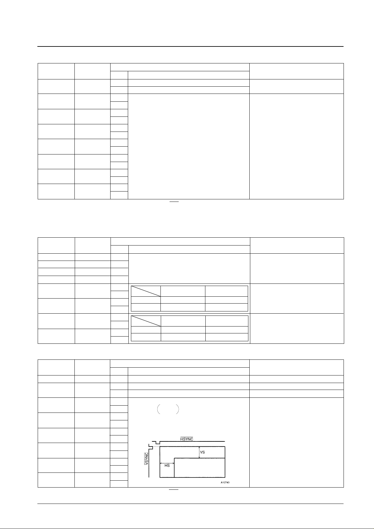
Figure 1 OSD Serial Data Input Timing
Figure 2 PDC/VPS Serial Timing (I2C bus)
No. 6018-7/35
LC74776, 74776M
S: Start condition
P: Stop condition
System Block Diagram
No. 6018-8/35
LC74776, 74776M
RAM write
address
counter
Display RAM
Deco-
der
Decoder
Font ROM
Display
control
register
Shift register
Character output control
Background control
Video output control
Sync signal generator
Blinking and
reverse
video control
register
Vertical
display
position
register
Horizontal
display
position
register
Blinking and
reverse video
control circuit
Vertical dot
counter
Horizontal
dot counter
Vertical display
position
detector
Line control
counter
Horizontal
display position
detector
Character
control
counter
Vertical size
counter
Horizontal
size counter
Vertical
character
size register
Horizontal
character
size register
Output control
Data output
buffer
Data
slicer
circuit
AFC
circuit
8-bit latch
+
command
decoder
Serial to
parallel
converter
Sync
discrimina-
tion
Character
output dot
clock
generator
Composite
sync signal
separation
control
Sync
separator
data
separator
circuit
Timing generator
Display Control Commands
Display control commands have an 8-bit format and are transferred using the serial input function. Commands consist of a
command identification code in the first byte and command data in the following bytes. The following commands are supported.
COMMAND0: Display memory (VRAM) write address setup command
COMMAND1: Display character data write command
COMMAND2: Vertical display start position and vertical character size setup command
COMMAND3: Horizontal display start position and horizontal character size setup command
COMMAND4: Display control setup command
COMMAND5: Display control setup command
COMMAND6: Synchronizing signal detection setup command
COMMAND7 to COMMAND12 and COMMAND18: Display control setup commands
COMMAND13 to COMMAND17: VPS/PDC control commands. These commands can only be written with the I2C bus
(the SCL and SDA pins).
Display Control Command Table
No. 6018-9/35
LC74776, 74776M
First byte Second byte
Command
Command identification code
Data Data
7 6 5 4 3 2 1 0 7 6 5 4 3 2 1 0
COMMAND0 1 0 0 0 V3 V2 V1 V0 0 0 0 H4 H3 H2 H1 H0
(Write address setup)
COMMAND1 1 0 0 1 0 0 0 0 at c6 c5 c4 c3 c2 c1 c0
(Character write)
COMMAND2 (Vertical character size and 1 0 1 0 VS VS VS VS 0 FS VP VP VP VP VP VP
vertical display start position) 21 20 11 10 5 4 3 2 1 0
COMMAND3 (Horizontal character size and 1 0 1 1 HS HS HS HS 0 LC HP HP HP HP HP HP
horizontal display start position) 21 20 11 10 5 4 3 2 1 0
COMMAND4 1 1 0 0 TST RAM OSC SYS 0 BLK BLK BLK BK BK RV DSP
(Display control) MOD ERS STP RST 2 1 0 1 0 ON
COMMAND5 1 1 0 1 NP NP NON INT 0 RSH HLF BCL CB PH PH PH
(Display control) 1 0 LV2 INT 2 1 0
COMMAND6 1 1 1 0 SEL MOD DIS MUT 0 RN RN RN SN SN SN SN
(Synchronizing signal detection) 0 0 LIN 2 1 0 3 2 1 0
COMMAND7 1 1 1 1 0 0 0 0 0 CIN CIN VNP VSP MSK MSK EGL
(Display control) SEL CTL SEL SEL ERS SEL
COMMAND8 1 1 1 1 0 0 0 1 0 LNA LNA LNA LNA LPA LPA LPA
(Display control) 3 2 1 0 2 1 0
COMMAND9 1 1 1 1 0 0 1 0 0 LNB LNB LNB LNB LPB LPB LPB
(Display control) 3 2 1 0 2 1 0
COMMAND10 1 1 1 1 0 0 1 1 0 LNC LNC LNC LNC LPC LPC LPC
(Display control) 3 2 1 0 2 1 0
COMMAND11 1 1 1 1 0 1 0 0 0 0 VSP VSP LNC MOD LNB MOD
(Display control) DCK SLC SEL 3 SEL 2
COMMAND12 1 1 1 1 0 1 0 1 0 0 OTD OTD HLF SEL OTH IND
(Display control) S1 S0 INT 2
COMMAND18 1 1 1 1 1 0 1 1 0 0 RNE SJN SJN SJN SJC SJC
(Display control) 0 3 2 1 1 0
COMMAND13 1 1 1 1 0 1 0 1 0 CPA CPA CPA VPM VPM VPM VPM
(VPS/PDC control) 2 1 0 3 2 1 0
COMMAND14 1 1 1 1 0 1 1 0 0 VMW VMW HBS HBS BMS EMS DCE
(VPS/PDC control) SE2 SEL 2 1
COMMAND15 1 1 1 1 0 1 1 1 0 0 ECV ECV ECV ECV ECV ECV
(VPS/PDC control) 15 14 13 12 11 5
COMMAND16 1 1 1 1 1 0 0 0 0 ECP ECP ECP ECP ECP ECP ECP
(VPS/PDC control) 19 18 17 16 15 14 13
COMMAND17 1 1 1 1 1 0 0 1 0 0 ECP ECP ECP ECP ECP ECP
(VPS/PDC control) 25 24 23 22 21 20
Once written, a first byte command identification code is stored until the next first byte is written. However, when the
display character data write command (COMMAND1) is written, the LC74776/M locks into the display character data
write mode, and another first byte cannot be written.
When the CS pin is set high, the LC74776/M is set to the COMMAND0 (display memory write address setup mode) state.

COMMAND0 (Display memory write address setup command)
No. 6018-10/35
LC74776, 74776M
DA 0 to 7 Register
Contents
Notes
State Function
7 – 1
6 – 0 Command 0 identification code.
5 – 0 Display memory write address setup.
4 – 0
3 V3
0
1
2 V2
0
1 Display memory line address (0 to B hexadecimal)
1 V1
0
1
0 V0
0
1
• First byte
DA 0 to 7 Register
Contents
Notes
State Function
7 – 0 Second byte identification bit
6 – 0
5 – 0
4 H4
0
1
3 H3
0
1
2 H2
0 Display memory column address (0 to 17 hexadecimal)
1
1 H1
0
1
0 H0
0
1
• Second byte
Note: All registers are set to 0 when the LC74776/M is reset by the RST pin.
DA 0 to 7 Register
Contents
Notes
State Function
7 – 1
When this command is input, the LC74776/M
6 – 0 Command 1 identification code.
locks in the display character data write mode
5 – 0 Display character data write mode setup.
until the CS pin goes high.
4 – 1
3 – 0
2 – 0
1 – 0
0 – 0
• First byte
COMMAND1 (Display character data write setup command)
No. 6018-11/35
LC74776, 74776M
DA 0 to 7 Register
Contents
Notes
State Function
7 at
0 Character attribute off
1 Character attribute on
6 c6
0
1
5 c5
0
1
4 c4
0
1 Character code (00 to FF hexadecimal)
3 c3
0
1
2 c2
0 (FE
HEX
: Space character)
1 (FF
HEX
: Transparent space character)
1 c1
0
1
0 c0
0
1
• Second byte
Note: All registers are set to 0 when the LC74776/M is reset by the RST pin.
DA 0 to 7 Register
Contents
Notes
State Function
7 – 1
6 – 0
Command 2 identification code.
5 – 1
Vertical display start position and the vertical character
4 – 0
size setup.
3 VS21
0
1
Second line vertical character size
2 VS20
0
1
1 VS11
0
1
First line vertical character size
0 VS10
0
1
COMMAND2: Vertical display start position and vertical character size setup command
VS20
0 1
VS21
0 1H/dot 2H/dot
1 3H/dot 1H/dot
VS10
0 1
VS11
0 1H/dot 2H/dot
1 3H/dot 1H/dot
DA 0 to 7 Register
Contents
Notes
State Function
7 – 0 Second byte identification bit
6 FS
0 Crystal oscillator frequency: 2fsc
1 Crystal oscillator frequency: 4fsc
5
VP5 0
(MSB) 1
4 VP4
0
1
3 VP3
0 The vertical display start position is set by the
1 6 bits VP0 to VP5.
2 VP2
0 The weight of bit 1 is 2H.
1
1 VP1
0
1
0
VP0 0
(LSB) 1
• Second byte
If VS is the vertical display start position then:
VS = α +H ×
H: The horizontal synchronization pulse period
α = 20H (525H systems)
α = 25H (625H systems)
2 ∑ 2 VP
n
5
n
n=0
Character display area
Note: All registers are set to 0 when the LC74776/M is reset by the RST pin.
• First byte
 Loading...