

SANYO LC74761M, LC74761 Datasheet
Ordering number :EN4846A
13096HA (OT)/N2894TH (OT) No. 4846-1/20
Overview
The LC74761 and LC74761M are on-screen display
CMOS LSIs that superimpose text and low-level graphics
onto a TV screen (video signal) under microcontroller.
The display characters have a 12 by 18 dots structure, and
256 characters are provided.
Features
• Display structure: 12 lines by 24 characters (up to 288
characters)
• Maximum character display: Up to 288 characters
• Character configuration: 12 (W) by 18 (H) dots structure
• Number of characters: 256 characters (254 plus space 1
font and transparent space 1 font)
• Character sizes: Three sizes (normal, double, and triple
sizes)
• Display starting positions: 64 horizontal and 64 vertical
locations
• Reverse video function: Characters can be inverted on a
per character basis.
• Flashing types: Two types with periods of 0.5 and 1.0
second on a per character basis (duty fixed at 50%)
• Background color: One of eight colors (when internal
synchronization used)
• External control input: Serial data input in 8-bit units
• Built-in horizontal/vertical sync separation circuit, AFC
circuit, and synchronization detector
• Video output: Composite video signal output in NTSC,
PAL, PAL-M, PAL-N, PAL60, NTSC4.43, or SECAM
format
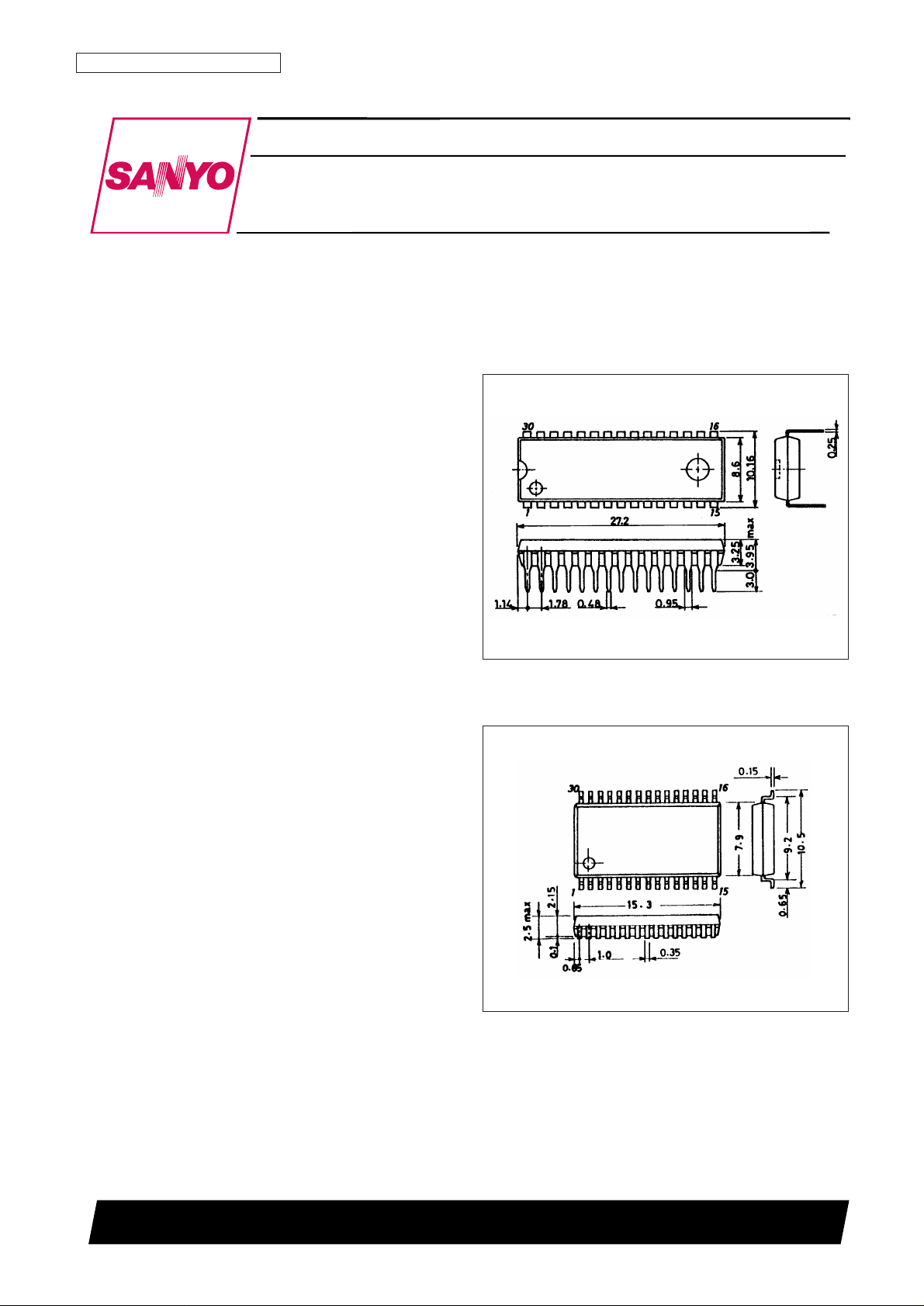
Package Dimensions
unit: mm
3196-DIP30SD
unit: mm
3216A-MFP30S
LC74761, 74761M
SANYO Electric Co.,Ltd. Semiconductor Bussiness Headquarters
TOKYO OFFICE Tokyo Bldg., 1-10, 1 Chome, Ueno, Taito-ku, TOKYO, 110-0005 JAPAN
On-Screen Display LSI
CMOS IC
SANYO: DIP30SD
[LC74761]
SANYO: MFP30S
[LC74761M]
Specifications
Absolute Maximum Ratings at Ta = 25°C
Parameter Symbol Conditions Ratings Unit
Maximum supply voltage V
DD
max V
DD1
, V
DD2
pins VSS– 0.3 to VSS+ 7.0 V
Maximum input voltage V
IN
max All input pins VSS– 0.3 to VDD+ 0.3 V
Maximum output voltage V
OUT
max
HSYNC
OUT
, VSYNC
OUT
,
V
SS
– 0.3 to VDD+ 0.3 V
SYNC
DET
pins
Allowable power dissipation Pd max 300 mW
Operating temperature Topr –30 to +70 °C
Storage temperature Tstg –40 to +125 °C
Allowable Operating Ranges at Ta = –30 to +70°C
Ratings
Parameter Symbol Conditions
min typ max
Unit
Supply voltage
V
DD1
V
DD1
pin 4.5 5.0 5.5 V
V
DD2
V
DD2
pin 4.5 5.0 1.27 V
DD1
V
Input high level voltage
V
IH1
RST, CS, SIN, SCLK pins 0.8 V
DD1
V
DD1
+ 0.3 V
V
IH2
SECAM, 525/625,
0.7 V
DD1
V
DD1
+ 0.3 V
NTSC/PAL, 3.58/4.43 pins
Input low level voltage
V
IL1
RST, CS, SIN, SCLK pins VSS– 0.3 0.2 V
DD1
V
V
IL2
SECAM, 525/625,
VSS– 0.3 0.3 V
DD1
V
NTSC/PAL, 3.58/4.43 pins
Input voltage V
IN
FC, AMPINpins VSS– 0.3 V
DD1
+ 0.3 V
V
IN1
CVIN pins 2 V
PP
V
Composite video signal input voltage V
IN2
CVCRpins 2 V
PP
V
V
IN3
SYNCINpins 2 V
PP
2.5 V
PP
V
Oscillator frequency
NTSC 14.318 MHz
F
OSC1
Xtal
IN1
, Xtal
OUT1
, Xtal
IN2
,
PAL 17.734 MHz
Xtal
OUT2
pins; 4fsc
PAL-M 14.302 MHz
PAL-N 14.328 MHz
Electrical Characteristics at Ta = –30 to +70°C, with V
DD1
= V
DD2
= 5 V unless otherwise specified
Ratings
Parameter Symbol Conditions
min typ max
Unit
Output off leakage current I
leak1
CV
OUT
pin 10 µA
Input off leakage current I
leak2
CVIN, CVCRpins 10 µA
Output high level voltage V
OH
HSYNC
OUT
, VSYNC
OUT
,
3.5 V
SYNC
DET
, SECAM, 525/625,
NTSC/PAL, 3.58/4.43, AMP
OUT
,
PD
OUT
pins; V
DD1
= 4.5 V, IOH= –1.0 mA
Output low level voltage V
OL
HSYNC
OUT
, VSYNC
OUT
,
1.0 V
SYNC
DET
, SECAM, 525/625,
NTSC/PAL, 3.58/4.43, AMP
OUT
,
PD
OUT
pins; V
DD1
= 4.5 V, IOL= 1.0 mA
Input current
I
IH
RST, CS, SIN, SCLK, SECAM, 525/625,
1 µA
NTSC/PAL, 3.58/4.43 pins; V
IN
= V
DD1
I
IL
SECAM, 525/625, NTSC/PAL,
–1 µA
3.58/4.43 pin; V
IN
= V
SS1
Oscillator frequency F
OSC3
VCOIN, VCO
OUT
pins; FC = 1/2 V
DD1
14.12 MHz
Operating current dissipation
I
DD1
V
DD1
pin; All outputs open, Xtal: 4fsc 15 mA
I
DD2
V
DD2
pin; V
DD2
= 5.0 V 20 mA
Timing Characteristics at Ta = –30 to +70°C, VDD= 5 ±0.5 V
Ratings
Parameter Symbol Conditions
min typ max
Unit
Minimum input pulse width
t
W(SCLK)
SCLK pin 200 ns
t
W(CS)
CS pin (during periods when CS is high) 1 µs
Data setup time
t
SU(CS)
CS pin 200 ns
t
SU(SIN)
SIN pin 200 ns
Data hold time
t
h(CS)
CS pin 2 µs
t
h(SIN)
SIN pin 200 ns
One word write time
t
word
Write time for 8 bits of data 4.2 µs
t
wt
RAM data write time 1 µs
No. 4846-2/20
LC74761, 74761M

Pin Functions
Pin No. Symbol Function Description
1 V
SS
Ground Ground connection
2 Xtal
IN1
Crystal oscillator connection
Connection for the crystal and capacitor used to form the crystal oscillator that generates
3 Xtal
OUT1
the internal synchronization signal. The oscillator can be selected with a command switch.
4 HSYNC
OUT
Horizontal synchronization Outputs the horizontal synchronization signal (AFC). The output polarity can be selected
output (metal option). Also functions as general output port (command switch).
5 Xtal
IN2
Crystal oscillator connection
Connection for the crystal and capacitor used to form the crystal oscillator that generates
6 Xtal
OUT2
the internal synchronization signal.
7 VSYNC
OUT
Vertical synchronization output
Outputs the vertical synchronization signal. The output polarity can be selected (metal
option). Also functions as general output port (command switch).
8 CS Enable input
Enables/disables serial data input. Serial data is enabled when this pin is low (hysteresis
input). Pull-up resistor built in (metal option).
9 SIN Data input Serial data input (hysteresis input). Pull-up resistor built in (metal option).
10 SCLK Clock input Clock input for serial data input (hysteresis input). Pull-up resistor built in (metal option).
SECAM mode switch input/
During input, switches between SECAM and other modes.
11 SECAM
output (command switch)
During output, functions as general output port or internal V output (command switch).
Low = other modes, high = SECAM mode
525/625 switch input/output
During input, switches between 525 scan lines and 625 scan lines.
12 525/625
(command switch)
During output, functions as general output port or character data output (command switch).
Low = 525 lines, high = 625 lines
NTSC/PAL switch input/output
Switches the color mode between NTSC and PAL.
13 NTSC/PAL
(command switch)
During output, functions as general output port or frame data output (command switch).
Low = NTSC, high = PAL
Switch FSC between 3.58 MHz and 4.43 MHz.
14 3.58/4.43 3.58/4.43 switch input/output During output, functions as general output port or half-tone output (command switch).
(command switch) Low = 3.58, high = 4.43
15 RST Reset input
System reset input pin, low is active (hysteresis input).
Pull-up resistor built in (metal option).
16 CV
OUT
Video signal output Composite video output
17 V
DD2
Power supply connection Power supply connection for composite video signal level generation
18 CV
IN
Video signal input Composite video input
19 CV
CR
Video signal input SECAM chroma signal input
20 SYNC
IN
Sync separator circuit input Built-in sync separator circuit video signal input
21 SEP
C
Sync separator circuit Built-in sync separator circuit
22 V
SS
Ground Ground connection
23 PD
OUT
Control voltage output AFC control voltage output
24 AMP
IN
AFC filter connection Filter connection
25 AMP
OUT
26 FC Control voltage input AFC control voltage input
27 VCO
IN
LC oscillator connection VCO LC oscillator circuit coil and capacitor connection
28 VCO
OUT
External synchronization signal
Outputs the exclusive NOR of the horizontal synchronization signal (AFC) and CSYNC (sync
29 SYNC
DET
detection output
separator). The output polarity can be selected (metal option). Also functions as general
output port (command switch).
30 V
DD1
Power supply connection Power supply connection (+5 V: digital system power supply)
No. 4846-3/20
LC74761, 74761M
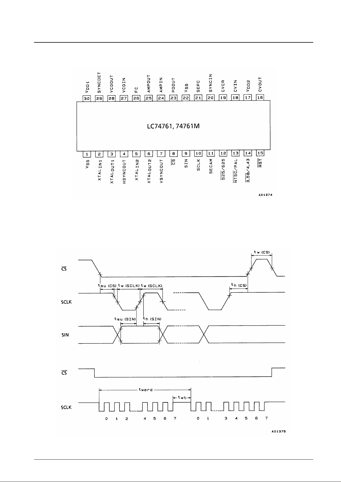
Pin Assignment
Serial Data Input Timing
No. 4846-4/20
LC74761, 74761M
Top view
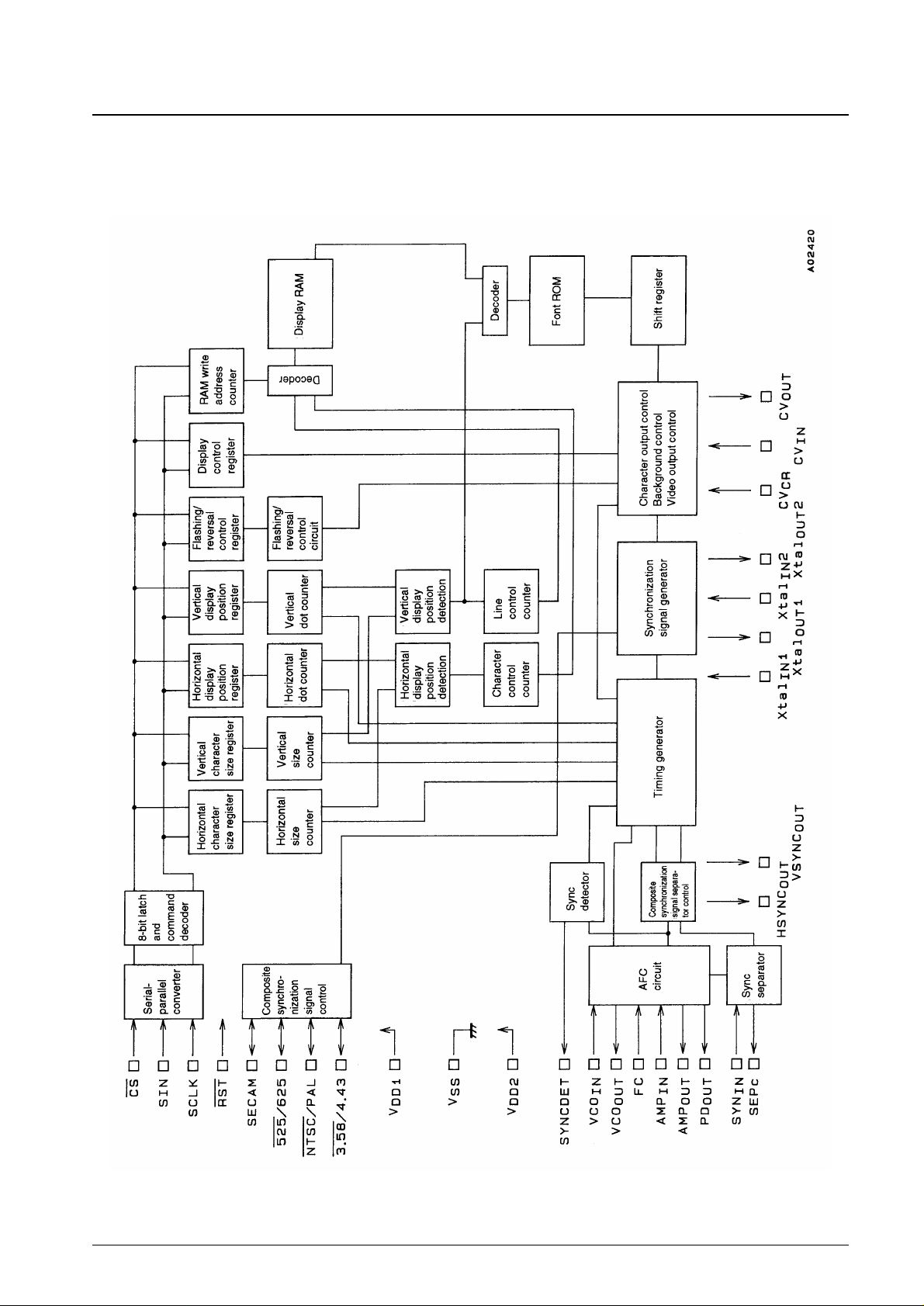
System Block Diagram
No. 4846-5/20
LC74761, 74761M

Display Control Commands
Display control commands are input in an 8-bit serial format. Commands consist of a command identification code in the
first byte and data in the second and following bytes. The following commands are supported.
1 COMMAND0: Display memory (VRAM) write address setting command
2 COMMAND1: Display character data write command
3 COMMAND2: Vertical display start position and character size (lines 1 and 2) setting command
4 COMMAND3: Horizontal display start position and character size (lines 9 and 11) setting command
5 COMMAND4: Display control setting command 1
6 COMMAND5: Display control setting command 2
7 COMMAND6: Display control setting command 3
8 COMMAND7: Display control setting command 4
Display Control Command Table
First byte Second byte
Command
Command identification code
Data Data
7 6 5 4 3 2 1 0 7 6 5 4 3 2 1 0
COMMAND0 1 0 0 0 V3 V2 V1 V0 0 0 0 H4 H3 H2 H1 H0
Write address
COMMAND1 1 0 0 1 0 0 at2 at1 c7 c6 c5 c4 c3 c2 c1 c0
Character write
COMMAND2 1 0 1 0 SZ SZ SZ SZ 0 0 VP VP VP VP VP VP
Vertical display start position 21 20 11 10 5 4 3 2 1 0
COMMAND3 1 0 1 1 SZ SZ SZ SZ 0 0 HP HP HP HP HP HP
Horizontal display start position B1 B0 91 90 5 4 3 2 1 0
COMMAND4 1 1 0 0 RST RAM OSC RND 0 I/N BLK BLK BK ATS 0 DSP
Display control 1 1 0 1
COMMAND5 1 1 0 1 PH PH PH I/E 0 TST CHAL BLK RSL RSL CVM XTS
Display control 2 2 1 0 1 0
COMMAND6 1 1 1 0 MOD MOD MOD MOD 0 HFI M30S SMS IOS BCL BCL CB
Display control 3 3 2 1 0 1 0
COMMAND70 1 1 1 1 0 0 0 LINS 0 VCOS LIN LIN LIN LIN LIN LIN
Display control 4 1 5 4 3 2 1 0
COMMAND71 1 1 1 1 0 1 0 LINS 0 EG PS PS VMN SVIS VNS VSS
Display control 5 2 2 1
COMMAND72 1 1 1 1 1 0 0 LINS 0 0 0 0 MOD MOD MOD MOD
Display control 6 3 2 1 0
COMMAND73 1 1 1 1 1 1 0 LINS 0 0 0 0 VCOS SOUT VOUT
HOUT
Display control 7 2
Once the command identification code in the first bite is written, it is stored internally until the first byte of the following
command is written. However, when the display character data write command (COMMAND1) is written, the system
becomes locked in display character data write mode, and the first byte cannot be overwritten.
When the CS pin is set high the command state is set to COMMAND0, i.e., display memory write address setting mode.
No. 4846-6/20
LC74761, 74761M
 Loading...