

SANYO LC74751 Datasheet
Overview
The LC74751 is a CMOS LSI that supports on-screen
display of characters and patterns on a TV screen under
the control of a microcontroller. The LC74751 includes an
on-chip character ROM that provides 128 characters in a
12 × 18 dot format. This IC supports display of up to 12
lines of 24 characters each for a maximum of 288
characters.
Features
• Display format: 24 characters by 12 rows
• Characters displayed: Up to 288 characters
• Display control ROM (line ROM): ROM for 64 lines
(Control in line units: lines consisting of 24 characters)
• Display RAM: 176 characters (Used for the specification
of user-defined characters.)
• Character format: 12 (horizontal) × 18 (vertical) dots
• Characters in font: 128
• Character sizes: Four sizes each in the horizontal and
vertical directions
• Initial display positions: 64 horizontal positions and 64
vertical positions
• Blinking: Specifiable in character units
• Blinking types:
— Two periods supported: 1.0 second and 0.5 second
— Three duty types supported: 25%, 50%, and 75%
• Blanking: Over the whole font (12 × 18 dots)
• Background color
— 8 background colors (in internal synchronization
mode): 4fsc (NTSC/PAL/PAL-M/PAL-N)
— 4 background colors (in internal synchronization
mode): 2fsc (NTSC)
— Single background color (blue) (in internal
synchronization mode): 2fsc (PAL/PAL-M/PAL-N)
• External control input: Serial data input
• Synchronizing signals: Supports switching between
internal and external synchronizing signals.
• On-chip sync separator circuit
• Video output: Composite video output in the NTSC,
PAL, PAL-M, or PAL-N format
• Superimpose function: Superimposes the character
output on the composite video output.
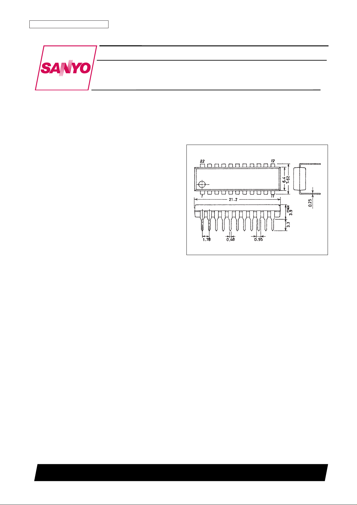
Package Dimensions
unit: mm
3059-DIP22S
CMOS LSI
Ordering number : EN*5396
83096HA (OT) No. 5396-1/15
Preliminary
SANYO: DIP22S
[LC74751]
SANYO Electric Co.,Ltd. Semiconductor Bussiness Headquarters
TOKYO OFFICE Tokyo Bldg., 1-10, 1 Chome, Ueno, Taito-ku, TOKYO, 110 JAPAN
On-Screen Display LSI
LC74751

Pin Assignment
No. 5396-2/15
LC74751
Parameter Symbol Conditions
Ratings
Unit
min typ max
Supply voltage
V
DD1VDD1
4.5 5.0 5.5 V
V
DD2VDD2
4.5 5.0 1.27 V
DD1
V
Input high-level voltage V
IH
CS, SIN, RST, SCLK, and SEP
IN
0.8 V
DD1
V
DD1
+ 0.3 V
Input low-level voltage V
IL
CS, SIN, RST, SCLK, and SEP
IN
V
SS
– 0.3 0.2 V
DD1
V
Composite video input voltage
V
IN1
CV
IN
2 Vp-p V
V
IN2
SYN
IN
2 Vp-p 2.5 Vp-p V
f
OSC1
Crystal oscillator pins (NTSC: 2fsc mode) 7.15909 MHz
f
OSC2
Crystal oscillator pins (NTSC: 4fsc mode) 14.31818 MHz
Oscillator frequency
f
OSC3
Crystal oscillator pins (PAL: 4fsc mode) 17.73447 MHz
f
OSC4
Crystal oscillator pins (PAL-M: 4fsc mode) 14.30244 MHz
f
OSC5
Crystal oscillator pins (PAL-N: 4fsc mode) 14.32822 MHz
f
OSC6
LC oscillator pin (When an LC oscillator is used)
5 7 11 MHz
Allowable Operating Ranges
Specifications
Absolute Maximum Ratings
Parameter Symbol Conditions Ratings Unit
Supply voltage V
DD
V
DD1
and V
DD2
VSS–0.3 to VSS+7.0 V
Input voltage V
IN
All input pins VSS–0.3 to VDD+0.3 V
Output voltage V
OUT
VSS–0.3 to VDD+0.3 V
Allowable power dissipation Pd max Ta = 25°C 300 mW
Operating temperature Topr –30 to +70 °C
Storage temperature Tstg –40 to +125 °C
Parameter Symbol Conditions
Ratings
Unit
min typ max
Output off leakage current I
leak
CV
OUT
10 µA
Output high-level voltage V
OH1
SEP
OUT
: V
DD1
= 4.5 V, IOH= –1.0 mA 3.5 V
Output low-level voltage V
OL1
SEP
OUT
: V
DD1
= 4.5 V, IOL= 1.0 mA 1.0 V
Input current
I
IH
CS, SIN, RST, SCLK, and SEPIN: VIN= V
DD1
1 µA
I
IL
OSCIN: VIN= V
SS
–1 µA
Operating current drain
I
DD1VDD1
; All outputs open, Xtal: 17.734MHz, LC = 7MHz
10 mA
I
DD2VDD2
; V
DD2
= 5.0 V 15 mA
Electrical Characteristics at Ta = –30 to +70°C, V
DD1
= 5 V unless otherwise specified
No. 5396-3/15
LC74751
Parameter Symbol Conditions
Ratings
Unit
min typ max
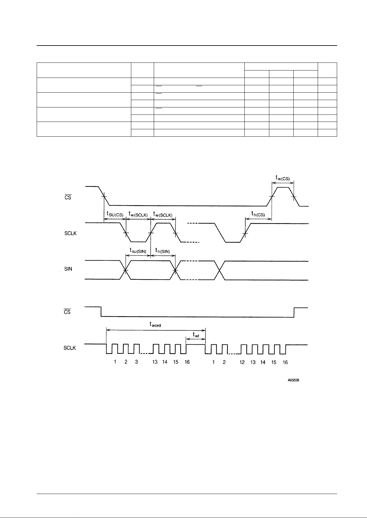
Minimum input pulse width
t
W(SCLK)
SCLK 200 ns
t
W(CS)
CS (the period when CS is high) 1 µs
Data setup time
t
SU(CS)
CS 200 ns
t
SU(SIN)
SIN 200 ns
Data hold time
t
h(CS)
CS 2 µs
t
h(SIN)
SIN 200 ns
One-word write time
t
word
The time to write 16 bits of data 10 µs
t
wt
The time to write data to RAM 1 µs
Timing Characteristics at Ta = –30 to +70°C, V
DD1
= 5±0.5 V
Serial Data Input Timing

Pin Functions
No. 5396-4/15
LC74751
Pin no. Pin Function Notes
1 V
SS
Ground Ground (digital system ground)
2 Xtal
IN
Crystal oscillator
Connections for the crystal and capacitors used to form the crystal oscillator for generating
3 Xtal
OUT
internal synchronizing signals.
4 TEST Test output Test data output
5 RST Reset input System reset input (This input has hysteresis characteristics.)
6 SCLK Clock input
Clock input for the serial data input function (This input has hysteresis characteristics.)
7 SIN Data input
Serial data input (This input has hysteresis characteristics.)
Data is input in 16-bit units.
8 CS Enable input
Serial data input enable input (This input has hysteresis characteristics.)
Serial data input is enabled when this pin is low.
9 LVBK Blanking level adjustment input Level input signal used to adjust the blanking level.
10 LVCHA Character level adjustment input Level input signal used to adjust the character level.
11 V
DD2
Power supply Composite video signal adjustment power supply (analog system power supply)
12 CV
OUT
Video signal output Composite video signal output
13 NC This pin must be either connected to ground or left open.
14 CV
IN
Video signal input Composite video signal input
15 V
DD1
Power supply Power supply (+5 V)
16 SYN
IN
Sync separator circuit input Input to the composite sync signal sync separator circuit
17 SEP
C
Sync separator circuit adjustment Sync separator circuit adjustment
18 SEP
OUT
Composite sync signal output Sync separator circuit composite sync signal output
19 SEP
IN
Vertical synchronizing signal input
Connect an integration circuit between the SEP
OUT
pin and this pin, which inputs the vertical
synchronizing signal, to integrate the output signal from the SEP
OUT
pin.
20 OSC
OUT
LC oscillator
Connections for the coil and capacitor that form the oscillator used to generate the character
21 OSC
IN
output dot clock.
22 V
DD1
Power supply (+5 V) Power supply (+5 V)
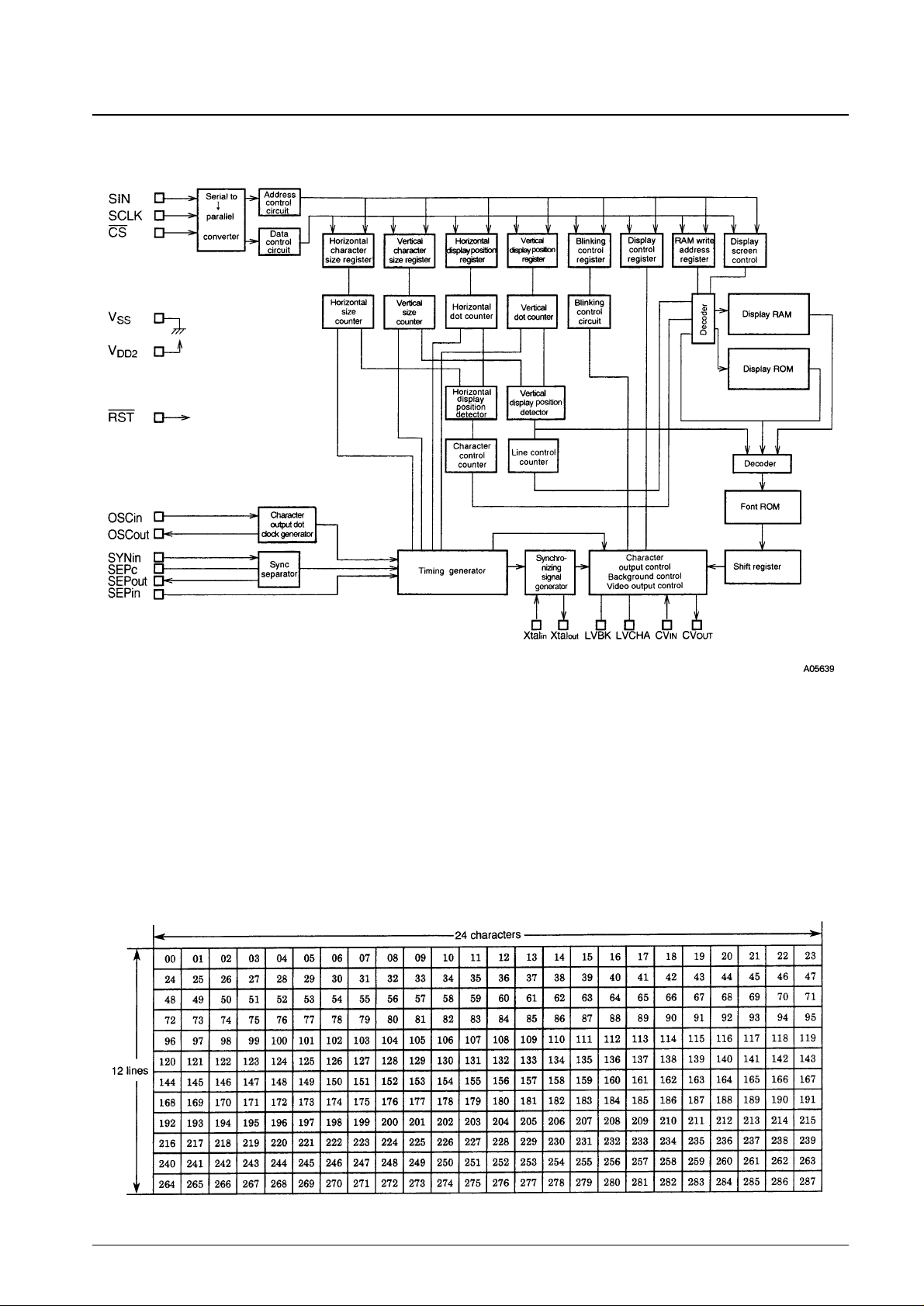
System Block Diagram
Display Screen Structure
The display mode has a 24-character by 12-row format.
The maximum number of characters that can be displayed is 288.
When character sizes are enlarged, the maximum number of characters that can be displayed is reduced.
Display ROM (12-line specification) and display RAM (for 176 characters)
• Specify fixed characters in the display line ROM.
• Application programs use the display RAM to specify characters for sections of the display in which the characters
change.
No. 5396-5/15
LC74751
 Loading...