

Ordering number : ENN*6526
63000RM (OT) No. 6526-1/38
Overview
The LC74731W and LC74732W are on-screen display
CMOS ICs that display characters and patterns on a TV
screen under the control of a microcontroller. These ICs
display 16 × 16-dot characters and up to 12 lines of text
with 24 characters per line.
Features
• Text structure: 12 lines × 24 characters (Up to 288
characters)
• Character format: 16 × 16 dots
Character display clock frequency: about 9 MHz
• Character sizes: Four sizes each in the horizontal and
vertical directions with the size set in line units.
• Number of characters supported:
LC74731W:256 (internal)
LC74732W:512 (internal)
Up to 8192 using an external ROM (for Japanese)
[Reference] JIS X0298 (1990): 6877 characters
JIS level 1 kanji: 2965 characters
JIS level 2 kanji: 3388 characters
Special characters: 524 characters
• Display start positions: 128 positions each in the
horizontal and vertical directions
• Blinking, reverse video, reversed blinking, and character
outlining: May be specified in individual character units.
• Blinking types: Two types with periods of about 1.0 and
about 0.5 seconds.
• Blanking: The whole font area (16 ×16 dots) can be
blanked in line units
(Four types: no blanking, character size blanking,
character plus outlining size blanking, and whole area up
to adjacent character blanking)
• Line spacing control: Zero to seven scan lines, in line
units
• Character color: Eight colors in character units (in
internal synchronization mode): 2 fsc and 4 fsc
(Black, red, green, yellow, blue, magenta, cyan, and
white)
• Character background color: Eight colors (in internal
synchronization mode): 2 fsc and 4 fsc
(Black, red, green, yellow, blue, magenta, cyan, and
transparent)
• Screen background color: Eight colors (in internal
synchronization mode): 2 fsc and 4 fsc
(Black, red, green, yellow, blue, magenta, cyan, and
white)
• External control inputs: Serial interface with an 8-bit
data size.
• Built-in sync separator circuit
• Video outputs: NTSC, PAL, PALM, PALN, NTSC
4.43, and PAL 60 composite video signal outputs
• Supports Y/C input
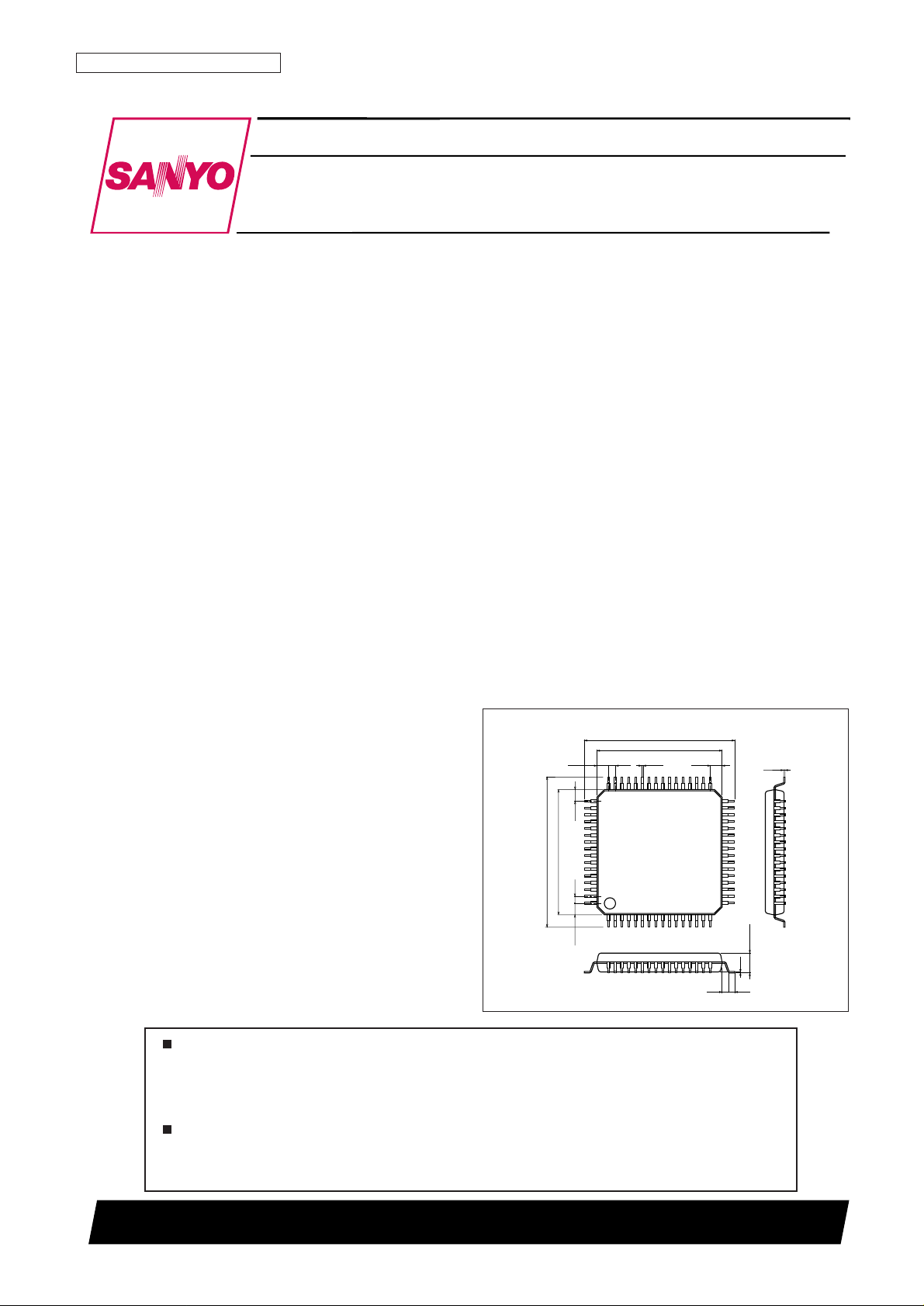
Package Dimensions
Preliminary
LC74731W,74732W
SANYO Electric Co.,Ltd. Semiconductor Company
TOKYO OFFICE Tokyo Bldg., 1-10, 1 Chome, Ueno, Taito-ku, TOKYO, 110-8534 JAPAN
On-Screen Display Controller
CMOS IC
Any and all SANYO products described or contained herein do not have specifications that can handle
applications that require extremely high levels of reliability, such as life-support systems, aircraft’s
control systems, or other applications whose failure can be reasonably expected to result in serious
physical and/or material damage. Consult with your SANYO representative nearest you before using
any SANYO products described or contained herein in such applications.
SANYO assumes no responsibility for equipment failures that result from using products at values that
exceed, even momentarily, rated values (such as maximum ratings, operating condition ranges, or other
parameters) listed in products specifications of any and all SANYO products described or contained
herein.
10.0
12.0
1.25
0.5
1.25
1.25 0.5 1.250.18
12.0
116
17
32
33
48
49
64
10.0
0.5
1.7max
0.5
0.1
0.15
SANYO: SQFP64
[LC74731W,74732W]
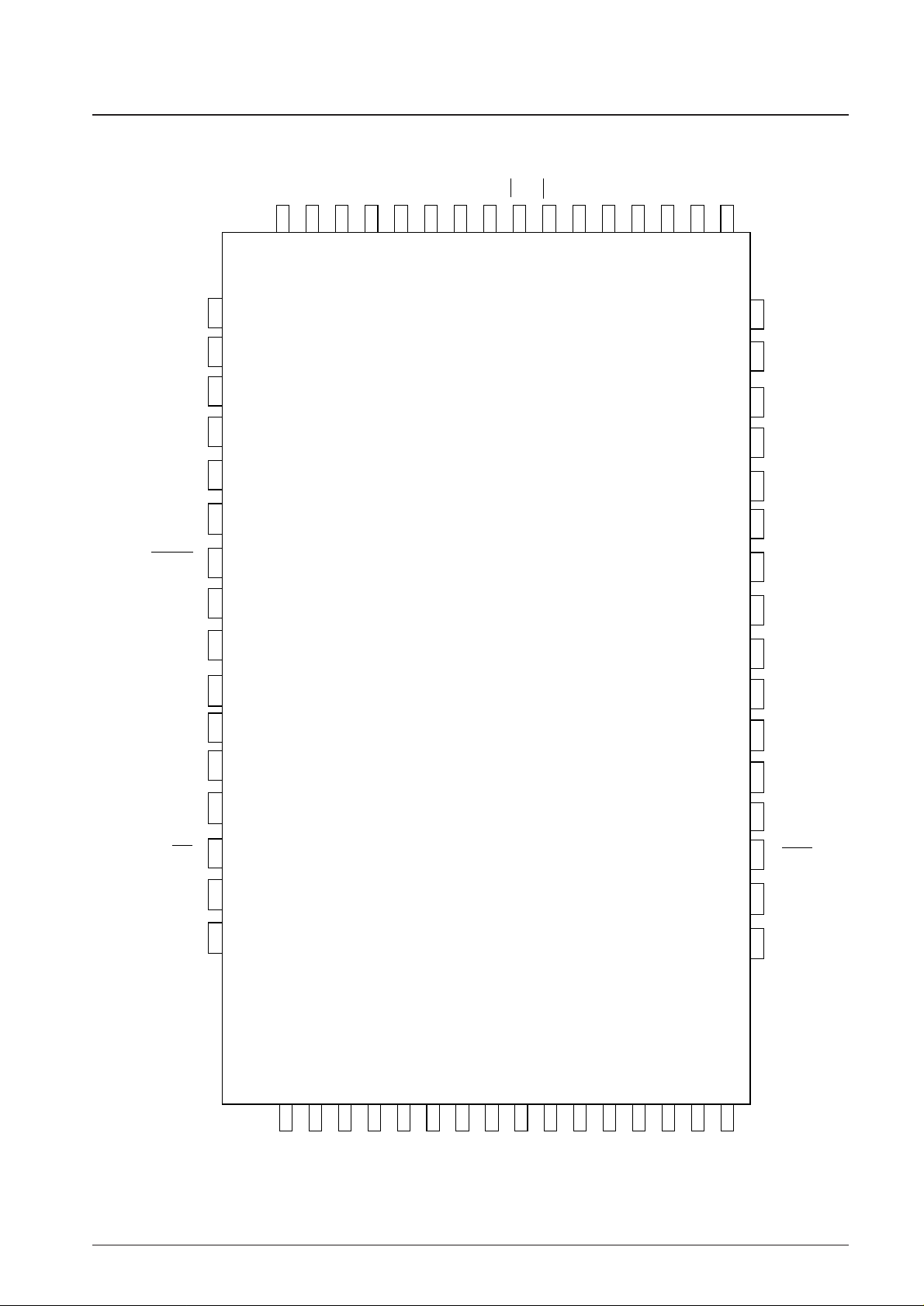
Pin Assignment
No. 6526-2/38
LC74731W,74732W
1VSS1
48
A6
2XTALin
47
A7
3XTALout
46
A8
4CTRL1
45
A9
5OSCin
44
A10
6OSCout
43
A11
7MUTE
42
A12
8CDLR
41
A13
9SYNCjdg/Rout
40
A14
10CHARA/Gout
39
A15
11BLANK/Bout
38
A16
12IEOUT/BLKout
37
A17
13OUTMOD
36
V
DD
1
14CS
35
RST
15SIN
(V) 34
SEPin
16SCLK
33
SEPout
(H)
Cout
Cin
-NC-
-NC-
V
SS
2
-NC-
CVcr
SYNin
V
DD
2
-NC-
Cbias
Yout
Yin
CVout
CVin
HFTin
17 18 19 20 21 22 23 24 25 26 27 28 29 30 31 32
63D162D261D360D459D558D657D756CE55OE54A053A152A251A350A449
A5
64
D0

No. 6526-3/38
LC74731W,74732W
Pin Functions
Pin No. Pin Function Description
1V
SS
1 Ground Ground connection. (Digital system ground)
2 Xtalin
Crystal oscillator connections
Connections for the crystal element and capacitors that form the internal sync signal generating
3 Xtalout
crystal oscillator. Xtalin can also be used to input an external clock signal. (2fsc or 4fsc)
4 CTRL1
Switches the crystal oscillator Selects external clock input mode or crystal oscillator mode. Low: crystal oscillator mode, high:
input external clock input mode.
5 OSCin
LC oscillator connections Connections for the coil and capacitor that form the character output dot clock generation oscillator.
6 OSCout
This is an active-low input with hysteresis characteristics (MORE+).
When low, the
7 MUTE Muting control input
CVout, Yout, and Cout outputs are set to either,
(1) CSYNC, CSYNC, PE, or
(2) PE PE, PE.
In the initial state, (1) is selected. This setting is switched by commands.
8 CDLR
Background color phase
Connection for the resistor used to adjust the background color phase
adjustment
Outputs the result of the judgment as to whether or not the external sync signal is present.
9
SYNCJDG External sync signal judgment A high level is output when a sync signal is present.
/Rout output (Rout output) The dot clock (LC oscillator) is output when RST is low.
(The IC can be set up to not output this signal during resets by commands.)
10 CHARA/Gout
Character output
Character signal output
(Gout output)
11 BLANK/Bout Blank output (Bout output) Blank signal output pin
12 IEout/BLKout
Internal/external output
Internal synchronization (high)/external synchronization (low) state output pin
(BLKout output)
13 OUTMOD Output switching input
Switches between output from pins 9 to 12 and input to pin 32.
Low: normal operation, high: RGB output supported
Serial data input enable
14 CS Enable input Serial data input is enabled when low.
more+ (Hysteresis input characteristics)
15 SIN Data input
Serial data input
more+ (Hysteresis input characteristics)
16 SCLK Clock input
Serial data input clock input
more+ (Hysteresis input characteristics)
17 V
DD
2 Power supply Composite video signal level adjustment power supply. (Analog system power supply)
18 COUT Color signal output Color (C) signal output
19 NC This pin must either be left open or connected to ground.
20 CIN Color signal input Color (C) signal input
21 CBIAS Chrominance bias output Chrominance signal bias level output
22 NC This pin must be either left open or connected to ground.
23 YOUT Luminance signal output Luminance signal (Y) output
24 NC This pin must be either left open or connected to ground.
25 YIN Luminance signal input Luminance signal (Y) input
26 V
SS
2 Ground Ground
27 CVOUT Video signal output Composite video signal output
28 NC This pin must either be left open or connected to ground.
29 CVIN Video signal input Composite video signal input
30 CVCR Video signal input SECAM chrominance signal input
31 HFTin Halftone signal input Halftone signal input
32 SYNin Sync separator circuit input Video signal input to the internal sync separator circuit
33 SEPout Composite sync signal output Composite sync signal output from the internal sync separator circuit
34 SEPin Vertical sync signal input
Vertical sync signal input
MORE+ (Hysteresis input characteristics)
35 RST Reset input
System reset input
A built-in pull-up resistor can be included in this pin’s input circuit. (Hysteresis input characteristics)
36 V
DD
1 Power supply (+5 V) Power supply (+5 V: digital system power supply)
Continued on next page.

No. 6526-4/38
LC74731W,74732W
Continued from preceding page.
Pin No. Pin Function Description
37 A17 Address output 17 ROM address output 17
38 A16 Address output 16 ROM address output 16
39 A15 Address output 15 ROM address output 15
40 A14 Address output 14 ROM address output 14
41 A13 Address output 13 ROM address output 13
42 A12 Address output 12 ROM address output 12
43 A11 Address output 11 ROM address output 11
44 A10 Address output 10 ROM address output 10
45 A9 Address output 9 ROM address output 9
46 A8 Address output 8 ROM address output 8
47 A7 Address output 7 ROM address output 7
48 A6 Address output 6 ROM address output 6
49 A5 Address output 5 ROM address output 5
50 A4 Address output 4 ROM address output 4
51 A3 Address output 3 ROM address output 3
52 A2 Address output 2 ROM address output 2
53 A1 Address output 1 ROM address output 1
54 A0 Address output 0 ROM address output 0
55 OE Output enable ROM output enable output. This is an active-low output.
56 CE Chip enable ROM chip enable output. This is an active-low output.
57 D7 Data input 7 ROM data input 7. MORE+ (Hysteresis input characteristics)
58 D6 Data input 6 ROM data input 6. MORE+ (Hysteresis input characteristics)
59 D5 Data input 5 ROM data input 5. MORE+ (Hysteresis input characteristics)
60 D4 Data input 4 ROM data input 4. MORE+ (Hysteresis input characteristics)
61 D3 Data input 3 ROM data input 3. MORE+ (Hysteresis input characteristics)
62 D2 Data input 2 ROM data input 2. MORE+ (Hysteresis input characteristics)
63 D1 Data input 1 ROM data input 1. MORE+ (Hysteresis input characteristics)
64 D0 Data input 0 ROM data input 0. MORE+ (Hysteresis input characteristics)
No. 6526-5/38
LC74731W,74732W
Specifications
Maximum Ratings at Ta = 25°C
Parameter Symbol Conditions
Ratings
Unit
min max
Supply voltage V
DDVDD
1 and VDD2V
SS
– 0.3 VSS+ 6.5 V
Input voltage V
IN
All input pins VSS– 0.3 VDD1 + 0.3 V
Output voltage V
OUT
SYNCJDG, BLANK, CHARA, SEPOUT, A0 to A17,
V
SS
– 0.3 VDD1 + 0.3 V
CE, and OE
Allowable power dissipation Pdmax — 275 mW
Operating temperature Topr –30 +70 °C
Storage temperature Tstg –40 +125 °C
Parameter Symbol Conditions
Ratings
Unit
min typ max
Supply voltage
V
DD
1VDD1 4.5 5.0 5.5 V
V
DD
2VDD2 4.5 5.0 6.5 V
Supply voltage
V
DD
1VDD1 2.7 5.0 5.5 V
[Only for RGB output]
V
DD
2VDD2 2.7 5.0 6.5 V
V
IH
1 CS, SIN, SCLK, SEPIN, and MUTE
0.8 VDD1
— 5.5 V
High-level input voltage
V
IH
2 RST
0.8 VDD1
—
VDD1 + 0.3
V
V
IH
3 CTRL1 and OUTMOD
0.7 VDD1
—
VDD1 + 0.3
V
V
IH
4 D0 to D7
0.8 VDD1
— 5.5 V
V
IL
1 RST, CS, SIN, SCLK, SEPIN, and MUTE VSS– 0.3 —
0.2 VDD1
V
Low-level input voltage V
IL
2 CTRL1 and OUTMOD VSS– 0.3 —
0.3 VDD1
V
V
IL
3 D0 to D7 VSS– 0.3 —
0.2 VDD1
V
Pull-up resistor R
PU
RST, CS, SIN, SCLK, and MUTE (when the pull-up
25 50 90 kΩ
resistor option is specified)
Composite video signal input
VIN1 CVIN and CVCR VDD1 = 5 V — 2.0 — Vp-p
voltage
V
IN
2 SYNIN VDD1 = 5 V 1.5 2.0 2.5 Vp-p
Input voltage V
IN
3
XtalIN (when an external clock input is used)
VDD1 = 5 V — — 5.0 Vp-p
fin = 2 fsc, 4 fsc
The XtalIN and XtalOUT oscillator pins (2 fsc: NTSC) 7.159 MHz
F
OSC1
The XtalIN and XtalOUT oscillator pins (4 fsc: NTSC) 14.318 MHz
Oscillator frequency The XtalIN and XtalOUT oscillator pins (2 fsc: PAL) — 8.867 — MHz
The XtalIN and XtalOUT oscillator pins (4 fsc: PAL) — 17.734 — MHz
F
OSC2
The OSCin and OSCout oscillator pins (LC oscillator) — 10 — MHz
Recommended Operating Conditions
Note: If the Xtalin pin is used in clock input mode, applications must take adequate input noise prevention and reduction measures.

No. 6526-6/38
LC74731W,74732W
Parameter Symbol Pin Conditions
Ratings
Unit
min typ max
Input off leakage current Ileak1 CV
IN
, CVCR, CIN, and Y
IN
—— 1µA
Output off leakage current Ileak2 CV
OUT
, C
OUT
, and Y
OUT
—— 1µA
V
OH
11
SYNCJDG, SETPOUT, V
DD
1 = 5.5 to 4.5 V
0.9 V
DD
1——V
BLANK, CHARA, and IEOUT I
OH
= –1.0 mA
V
OH
12
SYNCJDG, SETPOUT, V
DD
1 = 4.4 to 2.7 V
0.9 V
DD
1——V
High-level output voltage
BLANK, CHARA, and IEOUT I
OH
= –0.5 mA
V
OH
21 A0 to A17, OE, and CE
V
DD
1 = 5.5 to 4.5 V
0.9 V
DD
1——V
I
OH
= –1.0 mA
V
OH
22 A0 to A17, OE, and CE
V
DD
1 = 4.4 to 2.7 V
0.9 V
DD
1——V
I
OH
= –0.5 mA
V
OL
11
SYNCJDG, SEPOUT, V
DD
1 = 5.5 to 4.5 V
— — 0.1 V
DD
1V
BLANK, CHARA, and IEOUT I
OL
= 1.0 mA
V
OL
12
SYNCJDG, SEPOUT, V
DD
1 = 4.4 to 2.7 V
— — 0.1 V
DD
1V
Low-level output voltage
BLANK, CHARA, and IEOUT I
OL
= 0.5 mA
V
OL
21 A0 to A17, OE, and CE
V
DD
1 = 5.5 to 4.5 V
— — 0.1 V
DD
1V
I
OL
= 1.0 mA
V
OL
22 A0 to A17, OE, and CE
V
DD
1 = 4.4 to 2.7 V
— — 0.1 V
DD
1V
I
OL
= 0.5 mA
I
IH
RST, CS, SIN, SCLK, CTRL1,
V
IN
= VDD1——1µA
Input current
MUTE, and OUTMOD
I
IL
CS, SIN, SCLK, CTRL1, and
V
IN
= VSS1 –1——µA
OUTMOD
All outputs: open
Operating current drain
I
DD
1VDD1 Xtal: 17.734 MHz — — 40 mA
LC: 10 MHz
IDD2VDD2V
DD
2 = 5 V 20 mA
Electrical Characteristics at Ta = –30 to +70°C, VDD1 = 5 V unless otherwise specified.
Continued on next page.

No. 6526-7/38
LC74731W,74732W
Parameter Symbol Pin Conditions
Ratings
Unit
min typ max
(1) 0.80
SYNC level V
SN
(2) 1.00 V
(3) 1.40
(1) 1.37
Pedestal level V
PD
(2) 1.57
V
(3) 1.97
(1) 1.07
Color burst low level V
CBL
(2) 1.27
V
(3) 1.67
(1) 1.67
Color burst high level V
CBH
(2) 1.87
V
(3) 1.27
CVOUT
(1) 1.23
Background color 1 low level V
RSL
1
(1): When SYNC – LEVEL = 0.8 V
VDD1 = 5.0 V
(2) 1.43
V
(2): When SYNC – LEVEL = 1.0 V
VDD2 = 5.0 V
(3) 1.83
(3): When SYNC – LEVEL = 1.4 V
(1) 2.37
Background color 1 high level V
RSH
1
(2) 2.57
V
(3) 2.97
(1) 1.52
Background color 2 low level V
RSL
2
(2) 1.72
V
(3) 2.12
(1) 2.01
Background color 2 high level V
RSH
2
(2) 2.21
V
(3) 2.61
(1) 1.50
Outlining level 1 VBK1
(2) 1.70
V
(3) 2.10
(1) 1.80
Outlining level 2 VBK2
(2) 2.00
V
(3) 2.40
(1) 2.08
Outlining level 3 VBK3
(2) 2.28
V
(3) 2.68
(1) 2.65
Character level 1 V
CHA
1
(2) 2.85
V
(3) 3.25
(1) 2.23
Character level 3 V
CHA
3
(2) 2.43
V
(3) 2.83
Continued from preceding page.

Supplementary Materials
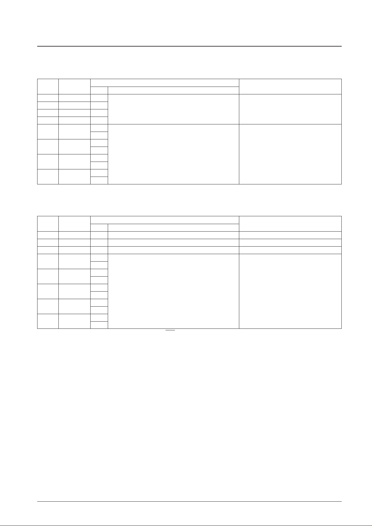
Figure 1 OSD Serial Data Input Timing
No. 6526-8/38
LC74731W,74732W
tw(cs)
CS
t
su
(cs) tw(sclk) tw(sclk) th(cs)
SCLK
t
su
(sin) th(sin)
SIN
t
word
t
wt
SCLK
01 567 01 5467
CS
Parameter Symbol Conditions
Ratings
Unit
min typ max
Minimum input pulse width
t
w
(sclk) SCLK 200 — — ns
t
w
(cs) CS (the period when CS is high) 1 — — µs
Data setup time
t
su
(cs) CS 200 — — ns
t
su
(sin) SIN 200 — — ns
Data hold time
t
h
(cs) CS 2 — — µs
t
h
(sin) SIN 200 — — ns
One word write time
t
word
The time to write 8 bits of data 4.2 — — µs
t
wt
RAM data write time 1 — — µs
OSD Write (See figure 1.) at Ta = –30 to +70°C, VDD1 = 5 ± 0.5 V
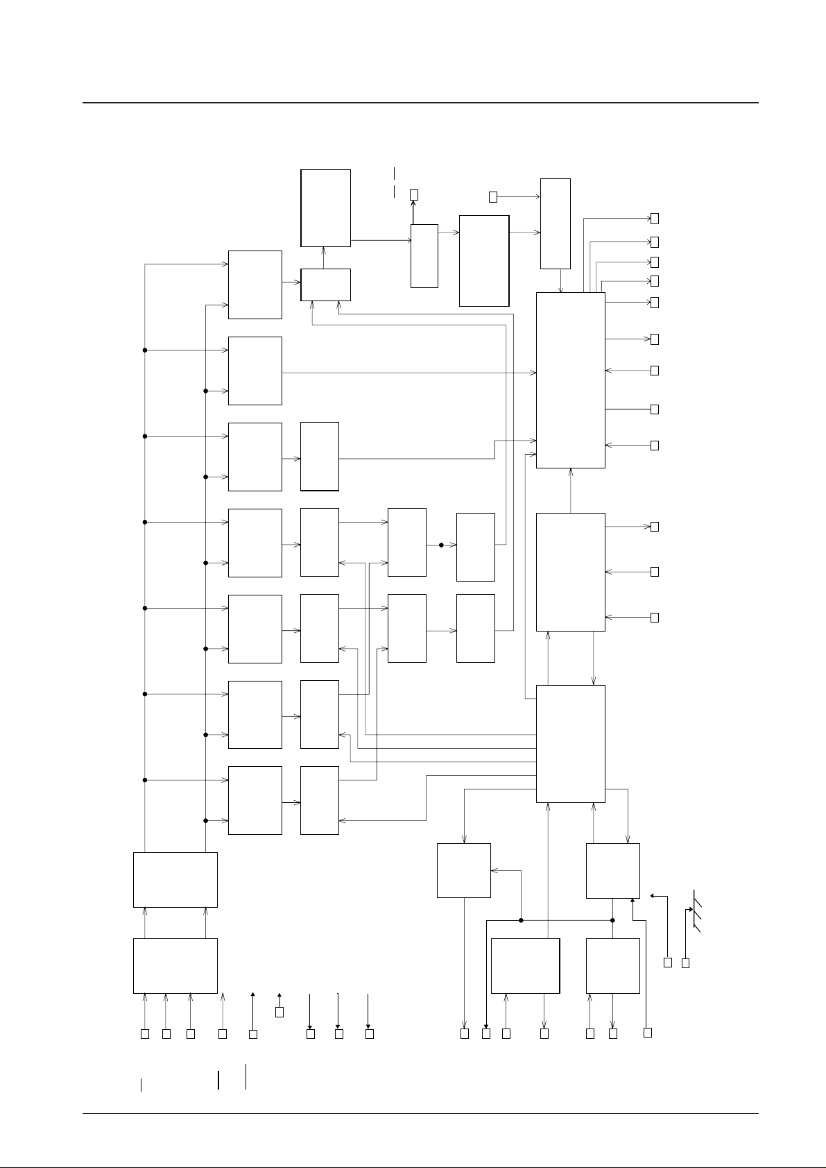
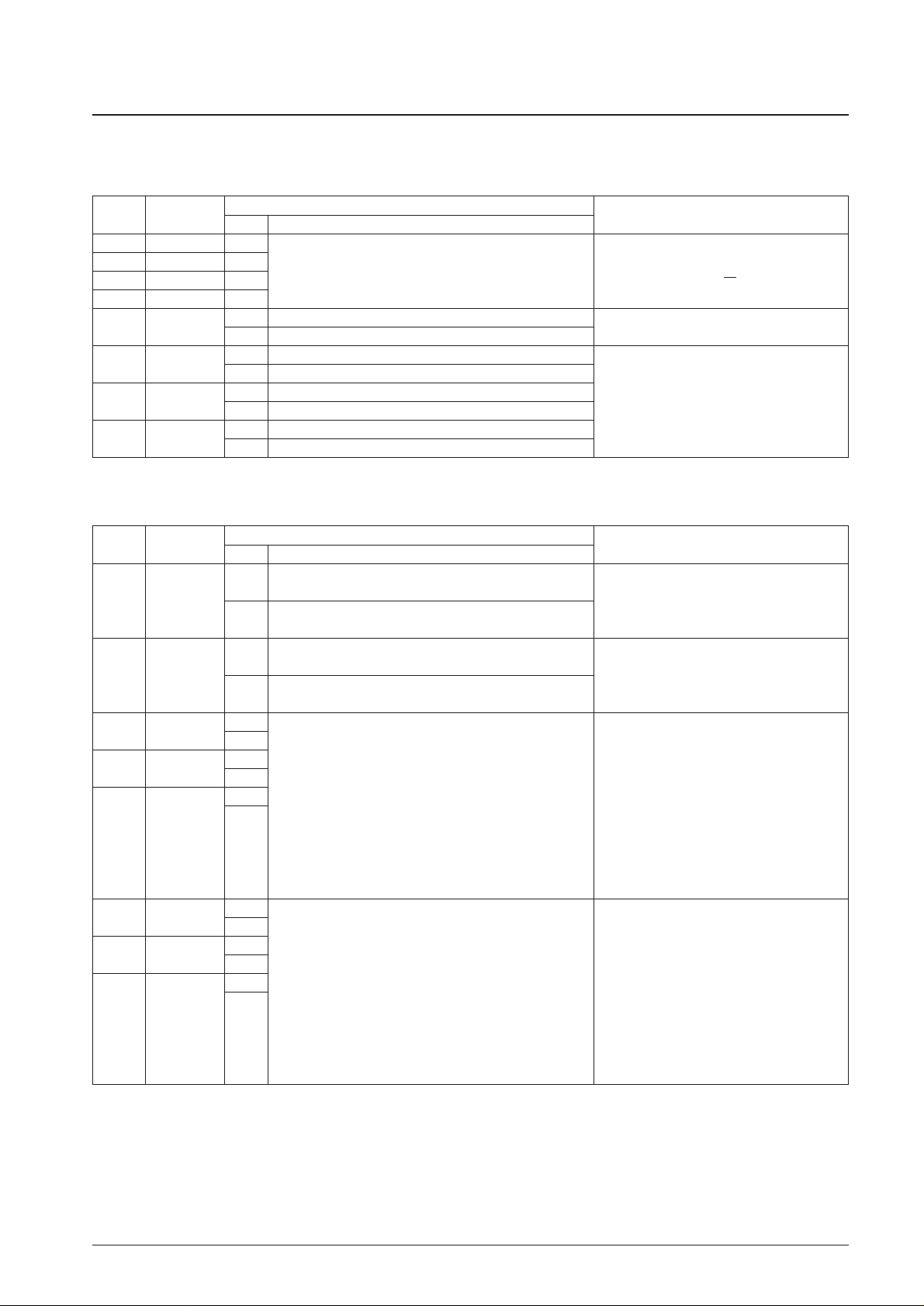
System Block Diagram
No. 6526-9/38
LC74731W,74732W
OSC IN
SYNC JDG
RST
OUTMOD
IEOUT
BLANK
CHARA
MUTE
SCLK
SIN
CS
SEP
C
SEP OUT
OSC OUT
SEP IN
SYN IN
VDD1, VDD2
VSS1, VSS2
CV OUTCDLR
C
IN Cbias
Yout
Yin
CV
INCTRL1 Xtal IN Xtal OUT CVCR Cout
Serial to
parallel
converter
Character
output
dot clock
oscillator
Synchronous
judgment
Composite
sync
separator
control
Sync
separator
circuit
8-bit
latch and
command
decoder
Horizontal
character
size register
Horizontal
size counter
Vertical
size counter
Timing generator
Horizontal
dot counter
Horizontal
display position
detection
Vertical
display position
detection
Character
control counter
Sync signal generator
Character output control
Background control
Video output control
Line control
counter
Vertical
dot counter
Blinking and
reverse video
control circuit
Vertical
character
size register
Horizontal
display
position register
Vertical
display
position register
Blinking and
reverse video
control register
Display control
register
RAM write
address counter
Display RAM
Decoder
Font ROM
Shift register
Decoder
A0 to A17,
OE, CE
D0 to D7

No. 6526-10/38
LC74731W,74732W
Display Control Commands
Display Control Commands
Display control commands have an 8-bit format and are transferred using the serial input function. Commands consist of
a command identification code in the first byte and command data in the following bytes.
First byte Second byte
Command
Command identification code
Data Data
7654321076543210
COMMAND0
1000V3V2V1V0000H4H3H2H1H0
(Write address setup)
at2 at1 CB2 CB1 CB0 CC2 CC1 CC0
COMMAND1 (Character write) 1001IRSD2SD1SD0000C12C11C10C9C8
C7 C6 C5 C4 C3 C2 C1 C0
COMMAND20
101000RRM1 RRM0 0 VP6 VP5 VP4 VP3 VP2 VP1 VP0
(Vertical display start position)
COMMAND21
101001000HP6HP5HP4HP3HP2HP1HP0
(Horizontal display start position)
COMMAND22
1010100SRM0000VS1VS0HS1HS0
(Character size)
COMMAND23
1010110
LSZUD
00
LSZB5 LSZA4 LSZ93 LSZ82 LSZ71 LSZ60
(Character size - in line units)
COMMAND3
1011
TSTMOD RAMERS OSCSTP SYSRST
0
LCSOFF XN53S BLKSEL
LC FS BK
DSPON
(Display control)
COMMAND4
1100NP2NP1NP0I/N0
HLFINT
BCL1 BCL0 CB PH2 PH1 PH0
(Display control)
COMMAND50
110100DISLIN I/E 0 RN2 RN1 RN0 SN3 SN2 SN1 SN0
(Sync signal detection 1)
COMMAND51
110101MUT1 MUT0 0 O RNE0 SJN3 SJN2 SJN1 SJC1 SJC0
(Sync signal detection 2)
COMMAND52
110110
EVEBSS LSPSS
0
CINSEL CINCTL VNPSEL VSPSEL MSKERS MSKSEL EGLSEL
(Display control)
COMMAND53
110111
RSLG1 RSLG0
00
CTL3 SPOSEL PALAL4 IHSEL VSSEL HSSEL
(Display control)
COMMAND60
1110000BRM0
BXBLV1 BXBLV0 BXWLV1 BXWLV0 ATSEL BLK1 BLK0
(Outlining setting)
COOMAND61
1110010
LFCUD
00
LFCB5 LFCA4 LFC93 LFC82 LFC71 LFC60
(Outlining setting - in line units)
COMMAND62
1110100GRM0OBXC1 GS1 GS0 GY2 GY1 GY0
(Line spacing)
COMMAND63
1110110
LGYUD
00
LGYB5 LGYA4 LGY93 LGY82 LGY71 LGY60
(Line spacing - in line units)
COMMAND70
1111000LRM00
BKLC1 BKLC0 CHLC1 CHLC0 RSLC1 RSLC0
(Display level)
COMMAND71
1111010
LCLUD
00
LCLB5 LCLA4 LCL93 LCL82 LCL71 LCL60
(Display level - in line units)
COMMAND72
111110
LHTDAT LHTUD
00LHTB5 LHTA4 LHT93 LHT82 LHT71 LHT60
(Halftone - in line units)
COMMAND73
111111000
DASSS GBSEL OUTSEL HSPSW XONSS BLK01 BLK00
(RGB control)
Note that when the display character data write command (COMMAND1) is written, tthese ICs lock into the display character data write mode, and another
first byte cannot be written.
When the CS pin is set high, the these ICs are set to the COMMAND0 (display memory write address setup mode) state.
COMMAND0 (Display memory write address setup command)
No. 6526-11/38
LC74731W,74732W
• First byte
DA0 to 7 Register
Content
Notes
State Function
7 — 1 Command 0 identification code
6 — 0 Display memory write address setup
5—0
4—0
3V3
0 Display memory line address (0 to B (hexadecimal))
1
2V2
0
1
1V1
0
1
0V0
0
1
• Second byte
Note that all registers are set to 0 when these ICs are reset by the RST pin.
DA0 to 7 Register
Content
Notes
State Function
7 — 0 Second byte identification code
6—0
5—0
4H4
0 Display memory line address (0 to 17 (hexadecimal))
1
3H3
0
1
2H2
0
1
1H1
0
1
0H0
0
1
No. 6526-12/38
LC74731W,74732W
COMMAND1 (Display character data write setup command)
• First byte
DA0 to 7 Register
Content
Notes
State Function
7—1
6 — 0 Command 1 identification code
5 — 0 Display character data write settings
4—1
3IR
0 Internal ROM Switching between internal and external ROM
1 External ROM
2 SD2
0 White-on-black (convex) display Character frame specification
1 Black-on-white (concave) display
1 SD1
0 Character frame start: off
1 Character frame start: on
0 SD0
0 Character frame stop: off
1 Character frame stop: on
• Second byte (1)
DA0 to 7 Register
Content
Notes
State Function
0
Character attribute 2: off Blinking specification
7 at2
(Character frame upper side: off) Selected by COM60 second byte and ATSEL.
1
Character attribute 2: on
(Character frame upper side: on)
0
Character attribute 1: off Reverse video specification
6 at1
(Character frame lower side: off) Selected by COM60 second byte and ATSEL.
1
Character attribute 1: on
(Character frame lower side: on)
5 cb2
0 cb2 cb1 cb0 Character background color Character background color specification
1(B G R)
4 cb1
0 0 0 0 Black
1 0 0 1 Red
0 0 1 0 Green
0 1 1 Yellow
3 cb0
1 0 0 Blue
1 1 0 1 Magenta
1 1 0 Cyan
1 1 1 Transparent
2 cc2
0 cc2 cc1 cc0 Character color Character color specification
1(B G R)
1 cc1
0 0 0 0 Black
1 0 0 1 Red
0 0 1 0 Green
0 1 1 Yellow
0 cc0
1 0 0 Blue
1 1 0 1 Magenta
1 1 0 Cyan
1 1 1 White
Note that when this command is input, the
LC74731W/74732W lock into the display character
data write mode until the CS pin is set high.
 Loading...