


Ordering number : EN*4247A
D3095HA (OT) No. 4247-1/14
Overview
The LC74730M is a CMOS LSI for on-screen display, a
function that displays characters and patterns on a TV
screen under microprocessor control. (The LC74730M
supports the S-VCR format.) The characters displayed
have an 8 × 8 dots structure and a dot interpolation
function is provided. The LC74730M display 10 lines of
24 characters each.
Features
• Screen format: 10 lines × 24 characters (up to 240
characters)
• Character format: 8 (horizontal) × 8 (vertical) (inter-
polation function provided)
• Character sizes: Three horizontal sizes and 3 vertical
sizes
• Number of characters in font: 64 characters
• Display start position
— Horizontal: 64 positions
— Vertical: 64 positions
• Blinking: In character units
• Types of blinking: Two types with approximately
1.0 sec. and 0.5 sec.
• Background color: Four background colors (in internal
synchronization mode)
(For the PAL-M format: 1 color; blue background)
• External control input: 8-bit serial data input format
• Built-in sync separator circuit
• Built-in synchronization recognition circuit: Recognizes
whether or not external synchronizing signals are
present
• Video output: NTSC and PAL-M format composite
outputs, Y-C output
Package Dimensions
unit: mm
3073A-MFP30S
Preliminary
SANYO: MFP30S
[LC74730M]
LC74730M
SANYO Electric Co.,Ltd. Semiconductor Bussiness Headquarters
TOKYO OFFICE Tokyo Bldg., 1-10, 1 Chome, Ueno, Taito-ku, TOKYO, 110-8534 JAPAN
On-Screen Display Controller LSI
CMOS LSI
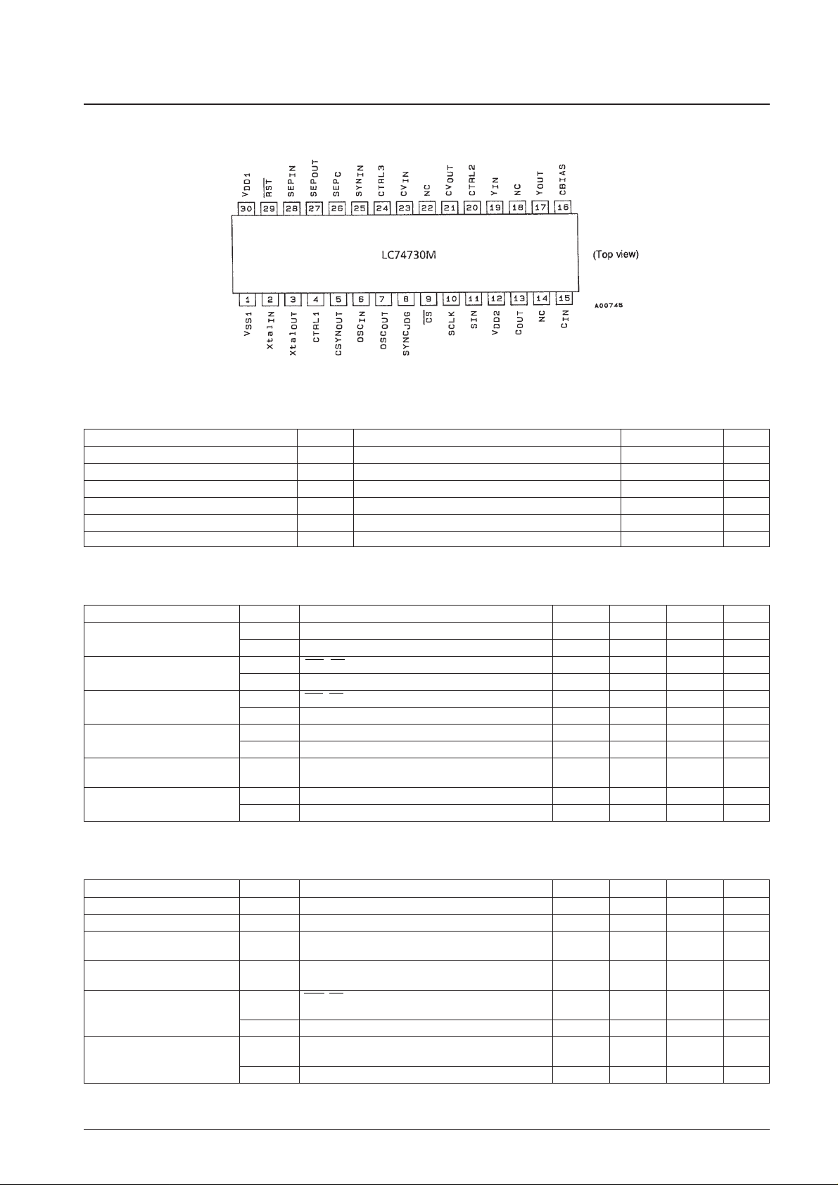
Pin Assignment
Specifications
Absolute Maximum Ratings at Ta = 25°C
Allowable Operating Ranges at Ta = –30 to +70°C
Electrical Characteristics at Ta = –30 to +70°C, unless otherwise specified VDD1 = 5 V
No. 4247-2/14
LC74730M
Parameter Symbol Conditions Ratings Unit
Maximum supply voltage V
DD
max VDD1, VDD2 VSS– 0.3 to VSS+ 7.0 V
Maximum input voltage V
IN
max All input pins VSS– 0.3 to VDD+ 0.3 V
Maximum output voltage V
OUT
max CSYN
OUT
, SYNC
JDG
, SEP
OUT
VSS– 0.3 to VDD+ 0.3 V
Allowable power dissipation Pd max 300 mW
Operating temperature Topr –30 to +70 °C
Storage temperature Tstg –40 to +125 °C
Parameter Symbol Conditions min typ max Unit
Supply voltage
V
DD
1 VDD1 4.5 5.0 5.5 V
V
DD
2 VDD2 4.5 5.0 1.27 VDD1 V
Input high-level voltage
V
IH
1 RST, CS, SIN, SCLK 0.8 VDD1 VDD1 + 0.3 V
V
IH
2 CTRL1 to CTRL3, SEP
IN
0.7 VDD1 VDD1 + 0.3 V
Input low-level voltage
V
IL
1 RST, CS, SIN, SCLK VSS– 0.3 0.2 VDD1 V
V
IL
2 CTRL1 to CTRL3, SEP
IN
VSS– 0.3 0.3 VDD1 V
Composite video input voltage
V
IN
1 CV
IN
2 Vp-p V
V
IN
2 SYN
IN
2 Vp-p 2.5 Vp-p V
Input voltage V
IN
3
The Xtal
IN
oscillator pin (in external clock input mode)
140 mV
Expected value (design target value)
Oscillator frequency
f
OSC
1 The XtalINand Xtal
OUT
oscillator pins (2fsc) 7.159 MHz
f
OSC
2 The OSCINand OSC
OUT
oscillator pins (LC oscillator) 5 8 12 MHz
Parameter Symbol Conditions min typ max Unit
Output off leakage current I
leak
1 C
OUT
, Y
OUT
, CV
OUT
10 µA
Input off leakage current I
leak
2 CIN, YIN, CV
IN
10 µA
Output high-level voltage V
OH
1
CSYN
OUT
, SYNC
JDG
, SEP
OUT
;
3.5 V
V
DD
1 = 4.5 V, IOH= 1.0 mA
Output low-level voltage V
OL
1
CSYN
OUT
, SYNC
JDG
, SEP
OUT
;
1.0 V
V
DD
1 = 4.5 V, IOL= 1.0 mA
I
IH
RST, CS, SIN, SCLK, CTRL1 to CTRL3, SEPIN;
1 µA
Input current
V
IN
= VDD1
I
IL
CTRL1 to CTRL3, OSCIN: VIN= VSS1 –1 µA
I
DD
1
V
DD
1; all outputs open, crystal: 7.159 MHz,
15 mA
Operating current drain
LC: 8 MHz
I
DD
2 VDD2; VDD2 = 5 V 20 mA

Timing Characteristics at Ta = –30 to +70°C, VDD1 = 5 ± 0.5 V
Pin Functions
No. 4247-3/14
LC74730M
Parameter Symbol Conditions min typ max Unit
Minimum input pulse width
t
W (SCLK)
SCLK 200 ns
t
W (CS)
CS pin (during the period that CS is high) 1 µs
Data setup time
t
SU (CS)
CS 200 ns
t
SU (SIN)
SIN 200 ns
Data hold time
t
h (CS)
CS 2 µs
t
h (SIN)
SIN 200 ns
One word write time
t
word
The 8-bit data write time 4.2 µs
t
wt
The RAM data write time 1 µs
Pin No. Symbol Function Description
1 V
SS
1 Ground Ground connection
2 Xtal
IN
Crystal oscillator element Used to connect the external crystal and capacitors for the crystal oscillator that generates
3 Xtal
OUT
connection the internal synchronizing signal. Also used for an external clock input. (2fsc: 7.159 MHz)
4 CTRL1
Crystal oscillator input Switches between the external 2f
sc
clock input mode and the crystal resonator driving mode.
switching Low: crystal oscillator, high: external clock input
5 CSYN
OUT
Composite synchronizing Outputs the composite synchronizing signal. Outputs the crystal oscillator clock on a reset due
signal output to a low level on the RST pin. Does not output any signal on a command reset.
6 OSC
IN
LC oscillator
Connections for the coil and capacitor that form the oscillator that generates the character
7 OSC
OUT
output dot clock.
External synchronizing signal
Outputs the judgment as to whether or not an external synchronizing signal is present. Outputs
8 SYNC
JDG
state judgment output
a high level when a synchronizing signal is present. Outputs the dot clock (LC oscillator) on a
reset due to a low level on the RST pin. Does not output any signal on a command reset.
9 CS Enable input
Enable input for serial data input. Serial data input is enabled by a low level. A pull-up resistor is
built in. (This input has hysteresis characteristics.)
10 SCLK Clock input Serial data input clock input. A pull-up resistor is built in. (This input has hysteresis characteristics.)
11 SIN Data input Serial data input. A pull-up resistor is built in. (This input has hysteresis characteristics.)
12 V
DD
2 Power supply Video signal level adjustment power supply. (Analog system power supply)
13 C
OUT
Color signal output Color (C) signal output
14 NC This pin must be level open or connected to ground.
15 C
IN
Color signal input Color (C) signal input
16 CBIAS Chrominance bias output Chrominance signal bias level output
17 Y
OUT
Luminance signal output Luminance signal (Y) output
18 NC This pin must be level open or connected to ground.
19 Y
IN
Luminance signal input Luminance signal (Y) input
20 CTRL2 NTSC/PAL-M switching input
Switches the synchronizing signal generator between NTSC and PAL-M formats. Low: NTSC,
high: PAL-M
21 CV
OUT
Composite video signal output Outputs a composite video signal.
22 NC This pin must be level open or connected to ground.
23 CV
IN
Composite video signal input Inputs a composite video signal.
24 CTRL3 SEP
IN
input control
Controls whether the VSYNC signal is input to the SEP
IN
input. Low: VSYNC is input,
high: VSYNC is not input.
25 SYN
IN
Sync separator circuit input
Video signal input to the built-in sync separator circuit. (Input either a horizontal or composite
synchronizing signal to this pin if the built-in sync separator circuit is not used.)
26 SEP
C
Sync separator circuit Adjusts the built-in sync separator circuit. (Connect a capacitor to this pin.)
adjustment (Leave this pin open if the built-in sync separator circuit is not used.)
27 SEP
OUT
Composite synchronizing Outputs the built-in sync separator circuit composite synchronizing signal.
signal output (Outputs the SYN
IN
input signal if the built-in sync separator circuit is not used.)
Vertical synchronizing
Integrates the SEP
OUT
output signal and inputs a vertical synchronizing signal.
28 SEP
IN
signal input
An integration circuit must be connected between this pin and the SEP
OUT
pin. This pin must
be tied to V
DD
1 if it is not used.
29 RST Reset input The system reset input. A pull-up resistor is built in. (This input has hysteresis characteristics.)
30 V
DD
1 Power supply (+5 V) Power supply (+5 V: digital system power supply)

Block Diagram
No. 4247-4/14
LC74730M
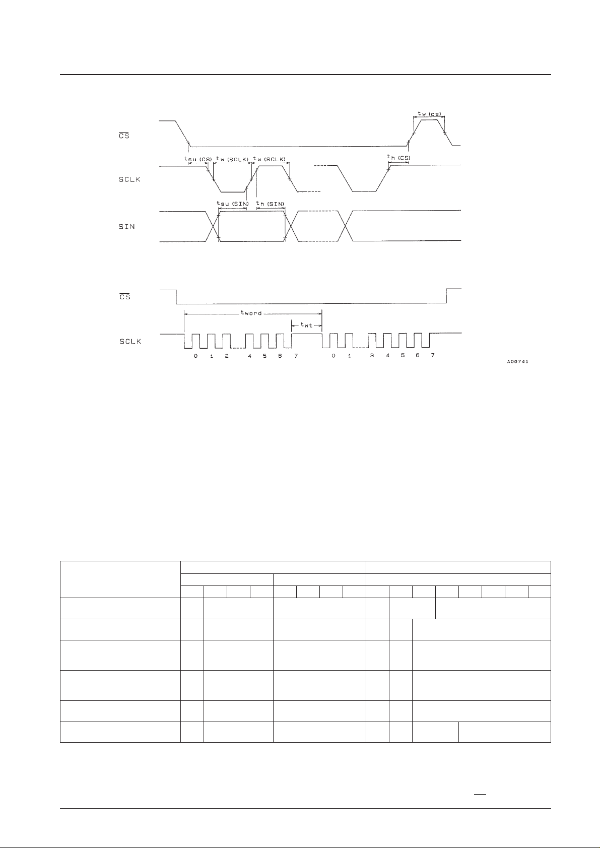
Serial Data Input Timing
Display Control Commands
The display control commands have an 8-bit serial input format. Commands consist of a first byte, which includes the
command identification code, and data in the second and following bytes. The LC74730M supports the following
commands:
① COMMAND 0: Display memory (VRAM) write address setup command
② COMMAND 1: Display character data write command
③ COMMAND 2: Vertical display start position and vertical size setup command
④ COMMAND 3: Horizontal display start position and horizontal size setup command
⑤ COMMAND 4: Display control setup command
⑥ COMMAND 5: Synchronizing signal control setup command
Display Control Command Table
The command identification code in a first byte is retained until the next first byte is written. However, if a display
character data write command (COMMAND 1) is written, the LC74730M locks in display character data write mode,
and the first byte cannot be overwritten.
The command state is reset to the COMMAND 0 state (display memory address setup mode) when the CS pin is set high.
No. 4247-5/14
LC74730M
First byte Second byte
Command
Command identification code
Data Data
7 6 5 4 3 2 1 0 7 6 5 4 3 2 1 0
COMMAND 0 1 0 0 0 V3 V2 V1 V0 0 0 0 H4 H3 H2 H1 H0
Set write address
COMMAND 1 1 0 0 1 0 0 0 0 at 0 c5 c4 c3 c2 c1 c0
Write character
COMMAND 2
1 0 1 0 VS VS VS VS 0 0 VP VP VP VP VP VP
Set vertical display start position and
21 20 11 10 5 4 3 2 1 0
vertical character size
COMMAND 3
1 0 1 1 HS HS HS HS 0 0 HP HP HP HP HP HP
Set horizontal display start position
21 20 11 10 5 4 3 2 1 0
and horizontal character size
COMMAND 4 1 1 0 0 TST CB OSC SYS 0 0 NON EG BK BK RV DSP
Display control MOD STP RST 1 0 ON
COMMAND 5 1 1 0 1 PH PH BCL INT 0 0 0 0 SN SN SN SN
Synchronizing signal control 1 0 3 2 1 0
 Loading...