

SANYO LC74725M, LC74725 Datasheet
Overview
The LC74725 and LC74725M are built-in EDS on-screen
display controller CMOS LSI products that display
characters and patterns on a TV screen under
microprocessor control. The characters displayed have an
8 × 8 dot format, and a dot interpolation function is
provided. These LSIs can display ten lines of
24 characters each.
Features
• Display format: 24 characters by 10 lines (up to
240 characters)
• Character format: 8 (horizontal) × 8 (vertical) dots
(interpolation function provided)
• Character sizes: Two horizontal and two vertical sizes
• Characters in font: 64 characters
• Initial display positions: 64 horizontal positions and
64 vertical positions
• Blinking: Specifiable on a per-character basis
• Blinking types: Two periods, 1.0 second and 0.5 second
• Blue background screen display: Available in internal
synchronization mode
• External control input: 8-bit serial input format
• Built-in sync separator circuit
• EDS support
• Video outputs: Composite video signal output in either
NTSC or PAL-M
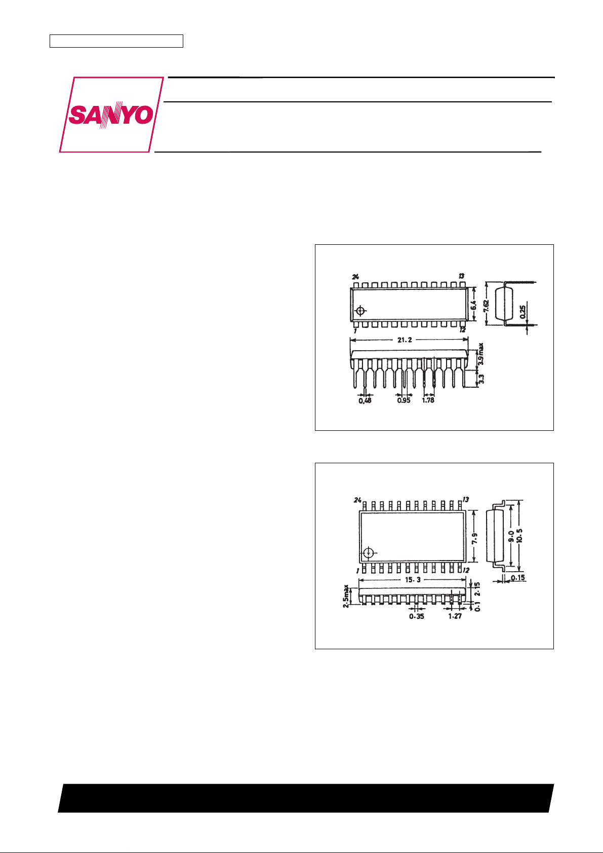
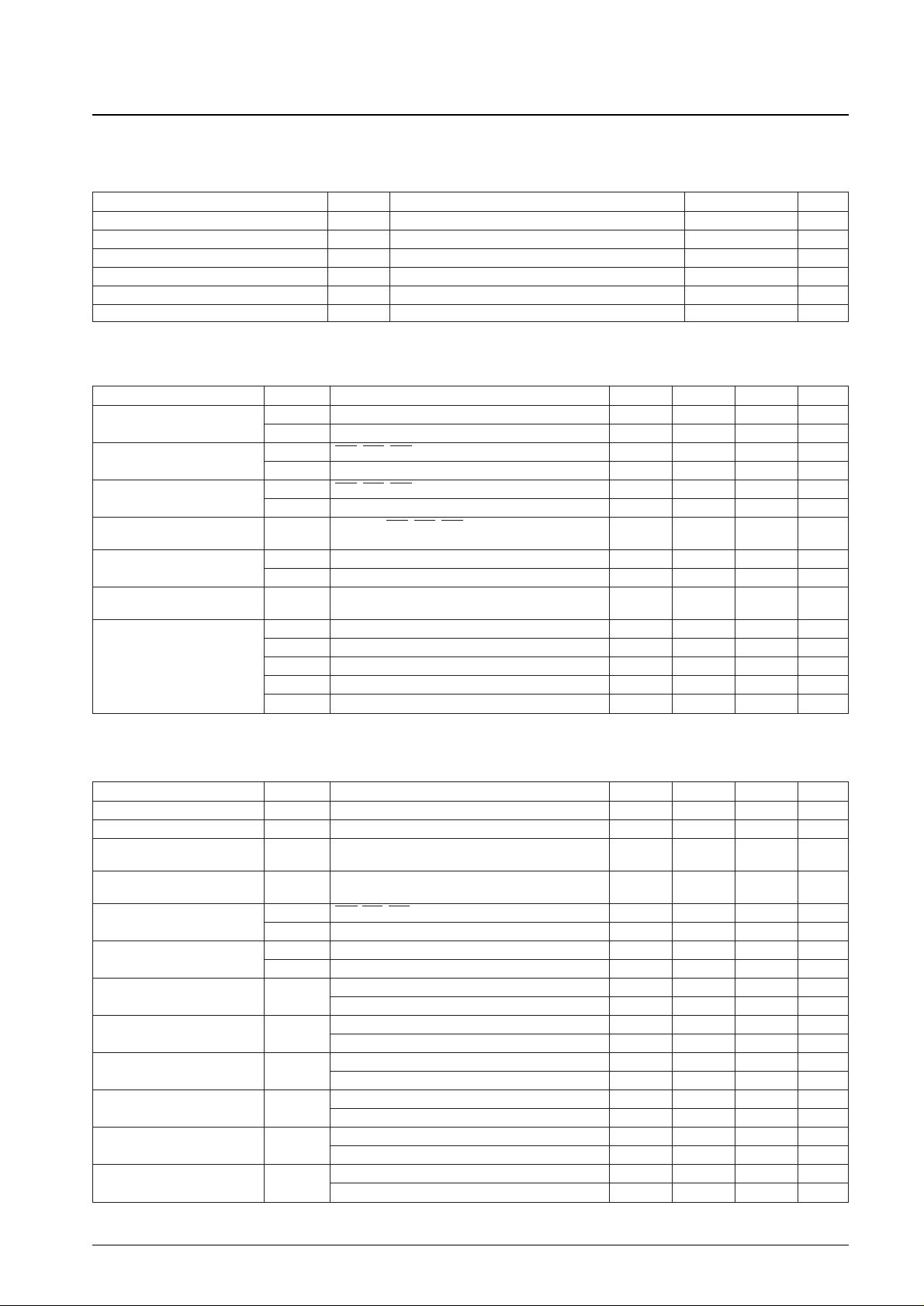
• Package: 24-pin plastic DIP (300 mil)
24-pin plastic MFP (375 mil)
Package Dimensions
unit: mm
3067-DIP24S
3045B-MFP24
CMOS LSI
41096HA (OT)/O3195HA (OT) No. 5213-1/16
SANYO: DIP24S
[LC7425]
SANYO: MFP24
[LC7425M]
SANYO Electric Co.,Ltd. Semiconductor Bussiness Headquarters
TOKYO OFFICE Tokyo Bldg., 1-10, 1 Chome, Ueno, Taito-ku, TOKYO, 110 JAPAN
On-Screen Display Controller LSI
LC74725, 74725M
Ordering number : EN5213A

No. 5213-2/16
LC74725, 74725M
Pin Assignment
Pin Functions
Note: Both VDD1 pins must be connected to the power supply.
Pin No. Symbol Function Description
1 V
SS
1 Ground Ground connection (digital system ground)
2 Xtal
IN
Connections for the external crystal and capacitors used to form a crystal oscillator for internal
Crystal oscillator synchronizing signal generation. Alternatively, these pins can be used for external clock input
3 Xtal
OUT
(2fsc or 4fsc).
4 CTRL1
Crystal oscillator input Switches between external clock input mode and crystal oscillator mode. Low: crystal oscillator
switching mode, high: external clock input mode.
5 LN21 Data output Line 21H pulse output (MOD0 = low: even field, MOD0 = high: both fields output)
6 OSC
IN
LC oscillator
Connections for the external coil and capacitor used to form the character output dot clock
7 OSC
OUT
generation oscillator.
Outputs the judgment as to where there are or are not external synchronizing signals present.
Outputs a high level when there are synchronizing signals.
External synchronizing
SEL0 = high: Outputs field discrimination pulses (O/E pulses)
8 SYNC
JDG
signal judgment output
Outputs the dot clock (LC oscillator) when the CS1 pin is high and the RST pin is low. A
command is provided that turns this output off.
Outputs the crystal oscillator clock when the CS1 pin is low and the RST pin is low. A
command is provided that turns this output off.
9 CS1 Enable input
Enable input for OSD serial data input. Serial data input is enabled when this pin is low. A pullup resistor is built in (hysteresis input).
10 SCLK Clock input
Serial data input clock input.
A pull-up resistor is built in (hysteresis input).
11 SIN Data input Serial data input. A pull-up resistor is built in (hysteresis input).
12 V
DD
2 Power supply Composite video signal level adjustment power supply (analog system power supply)
13 CV
OUT
Video signal output Composite video signal output pin
14 NC Must be either connected to ground or left open.
15 CV
IN
Video signal input Composite video signal input pin
16 V
DD
1 Power supply Power supply (+5 V: digital system power supply)
17 SYN
IN
Sync separator circuit input Video signal input to the built-in sync separator circuit
18 V
SS
1 Ground Ground (digital system ground)
19 SEP
OUT
Composite synchronizing
Video signal output from the built-in sync separator circuit
signal output
Vertical synchronizing
Inputs the vertical synchronizing signal generated by integrating the SEP
OUT
pin output signal.
20 SEP
IN
signal input
An integrating circuit must be inserted between the SEP
OUT
pin and this pin. This pin must be
tied to V
DD
1 if unused.
21 CS2 Enable input
Enable input for EDS data output. EDS data output is enabled when this input is low. A pull-up
resistor is built in (hysteresis input).
22 CPDT Data output EDS data output (either an n-channel open-drain or a CMOS output circuit)
23 RST Reset input System reset input. A pull-up resistor is built in (hysteresis input).
24 V
DD
1 Power supply (+5 V) Power supply (+5 V: digital system power supply)
No. 5213-3/16
LC74725, 74725M
Specifications
Absolute Maximum Ratings at Ta = 25°C
Allowable Operating Ranges at Ta = –30 to +70°C
Note: Extreme care must be used to prevent noise when the XtalINpin is used in clock input mode.
Electrical Characteristics at Ta = –30 to +70°C, and unless otherwise specified, with VDD1 = 5 V
Parameter Symbol Conditions Ratings Unit
Maximum supply voltage V
DD
max VDD1, VDD2 VSS– 0.3 to VSS+ 7.0 V
Maximum input voltage V
IN
max All input pins VSS– 0.3 to VDD+ 0.3 V
Maximum output voltage V
OUT
max LN21, CPDT, SEP
OUT
, SYNC
JDG
VSS– 0.3 to VDD+ 0.3 V
Allowable power dissipation Pd max Ta = 25°C 350 mW
Operating temperature Topr –30 to +70 °C
Storage temperature Tstg –40 to +125 °C
Parameter Symbol Conditions min typ max Unit
Supply voltage
V
DD
1 VDD1 4.5 5.0 5.5 V
V
DD
2 VDD2 4.5 5.0 1.27 VDD1 V
Input high level voltage
V
IH
1 RST, CS1, CS2, SIN, SCLK 0.8 VDD1 VDD1 + 0.3 V
V
IH
2 CTRL1, SEP
IN
0.7 VDD1 VDD1 + 0.3 V
Input low level voltage
V
IL
1 RST, CS1, CS2, SIN, SCLK VSS– 0.3 0.2 VDD1 V
V
IL
2 CTRL1, SEP
IN
VSS– 0.3 0.3 VDD1 V
Pull-up resistance
R
PU
Applies to RST, CS1, CS2, SIN, SCLK, and the pins
25 50 90 kΩ
specified as options.
Composite video input voltage
V
IN
1 CVIN: VDD1 = 5 V 2.0 Vp-p
V
IN
2 SYNIN: VDD1 = 5 V 1.5 2.0 2.5 Vp-p
Input voltage V
IN
3
Xtal
IN
(when external clock input is used),
0.1 5.0 Vp-p
f
IN
= 2fsc or 4fsc: VDD1 = 5 V
f
OSC
1 XtalIN, Xtal
OUT
oscillator pins (2fsc: NTSC) 7.159 MHz
f
OSC
1 XtalIN, Xtal
OUT
oscillator pins (4fsc: NTSC) 14.318 MHz
Oscillator frequency f
OSC
1 XtalIN, Xtal
OUT
oscillator pins (2fsc: PAL-M) 7.151 MHz
f
OSC
1 XtalIN, Xtal
OUT
oscillator pins (4fsc: PAL-M) 14.302 MHz
f
OSC
2 OSCIN, OSC
OUT
oscillator pins (LC oscillator) 5 12 MHz
Parameter Symbol Conditions min typ max Unit
Input off leakage current I
leak
1 CV
IN
1 µA
Output off leakage current I
leak
2 CV
OUT
1 µA
Output high level voltage V
OH
1
LN21, SYNC
JDG
, CPDT, SEP
OUT
: VDD1 = 4.5 V,
3.5 V
I
OH
= –1.0 mA
Output low level voltage V
OL
1
LN21, SYNC
JDG
, CPDT, SEP
OUT
: VDD1 = 4.5 V,
1.0 V
I
OL
= 1.0 mA
Input current
I
IH
RST, CS1, CS2, SIN, SCLK, CTRL1, SEPIN: VIN= VDD1 1 µA
I
IL
CTRL1, OSCIN: VIN= VSS1 –1 µA
Operating current drain
I
DD
1 VDD1: All outputs open, crystal: 7.159 MHz, LC: 8 MHz 30 mA
I
DD
2 VDD2: VDD2 = 5 V 20 mA
Sync level V
SN
When the sync level is 0.8 V, CV
OUT
: VDD1, VDD2 = 5 V 0.69 0.81 0.98 V
When the sync level is 1.0 V, CV
OUT
: VDD1, VDD2 = 5 V 0.89 1.01 1.13 V
Pedestal level V
PD
When the sync level is 0.8 V, CV
OUT
: VDD1, VDD2 = 5 V 1.28 1.40 1.52 V
When the sync level is 1.0 V, CV
OUT
: VDD1, VDD2 = 5 V 1.47 1.59 1.71 V
Color burst low level V
CBL
When the sync level is 0.8 V, CV
OUT
: VDD1, VDD2 = 5 V 0.97 1.09 1.21 V
When the sync level is 1.0 V, CV
OUT
: VDD1, VDD2 = 5 V 1.16 1.28 1.40 V
Color burst high level V
CBH
When the sync level is 0.8 V, CV
OUT
: VDD1, VDD2 = 5 V 1.60 1.72 1.84 V
When the sync level is 1.0 V, CV
OUT
: VDD1, VDD2 = 5 V 1.79 1.91 2.03 V
Background color low level V
RSL
When the sync level is 0.8 V, CV
OUT
: VDD1, VDD2 = 5 V 1.44 1.56 1.68 V
When the sync level is 1.0 V, CV
OUT
: VDD1, VDD2 = 5 V 1.63 1.75 1.87 V
Background color high level V
RSH
When the sync level is 0.8 V, CV
OUT
: VDD1, VDD2 = 5 V 1.96 2.08 2.20 V
When the sync level is 1.0 V, CV
OUT
: VDD1, VDD2 = 5 V 2.16 2.28 2.40 V
Continued on next page.
No. 5213-4/16
LC74725, 74725M
Continued from preceding page.
Timing Characteristics at Ta = –30 to +70°C, VDD1 = 5 V ± 0.5 V
Note: Follows the OSD timing for the CMOS output circuit type.
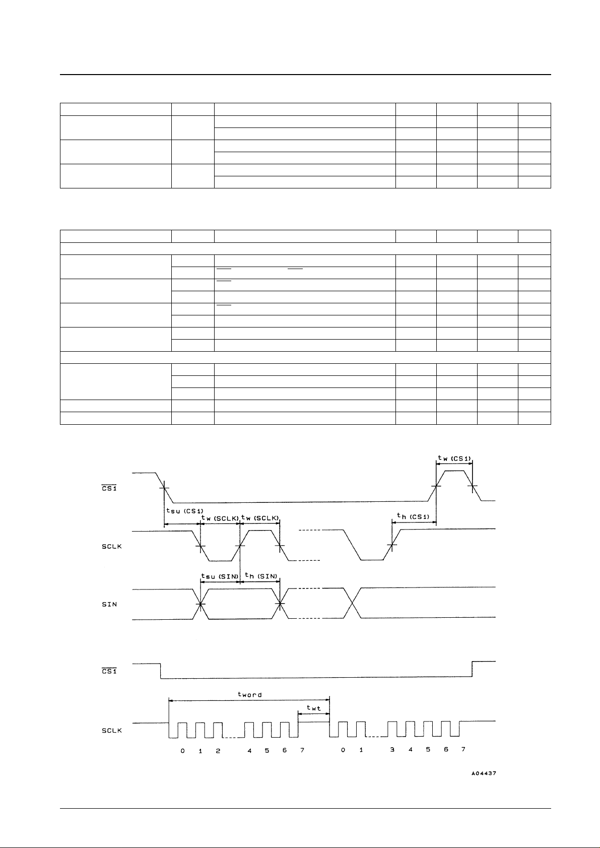
Figure 1 OSD Serial Data Input Timing
Parameter Symbol Conditions min typ max Unit
Border level 0 V
BK0
When the sync level is 0.8 V, CV
OUT
: VDD1, VDD2 = 5 V 1.43 1.55 1.67 V
When the sync level is 1.0 V, CV
OUT
: VDD1, VDD2 = 5 V 1.61 1.73 1.85 V
Border level 1 V
BK1
When the sync level is 0.8 V, CV
OUT
: VDD1, VDD2 = 5 V 2.01 2.13 2.25 V
When the sync level is 1.0 V, CV
OUT
: VDD1, VDD2 = 5 V 2.18 2.30 2.42 V
Character level V
CHA
When the sync level is 0.8 V, CV
OUT
: VDD1, VDD2 = 5 V 2.57 2.69 2.81 V
When the sync level is 1.0 V, CV
OUT
: VDD1, VDD2 = 5 V 2.76 2.88 3.00 V
Parameter Symbol Conditions min typ max Unit
OSD write (See Figure 1.)
Minimum input pulse width
t
W (SCLK)
SCLK 200 ns
t
W (CS1)
CS1 (the period when CS1 is high) 1 µs
Data setup time
t
SU (CS1)
CS1 200 ns
t
SU (SIN)
SIN 200 ns
Data hold time
t
h (CS1)
CS1 2 µs
t
h (SIN)
SIN 200 ns
One-word write time
t
word
The time to write 8 bits of data 4.2 µs
t
wt
The RAM data write time 1 µs
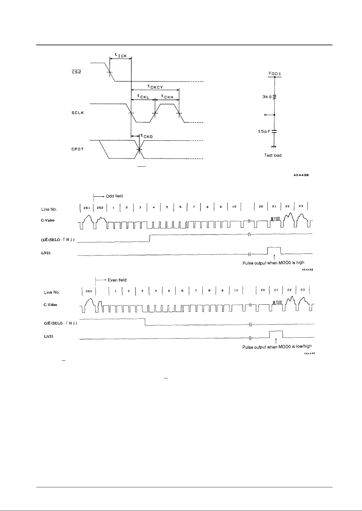
ESD read (See Figure 2 for the n-channel open-drain circuit.)
t
CKCY
SCLK 2 ns
Minimum input pulse width t
CKL
SCLK 1 µs
t
CKH
SCLK 1 µs
Data setup time t
ICK
SCLK 10 µs
Output delay time t
CKO
CPDT 0.5 µs
No. 5213-5/16
LC74725, 74725M
Note: CPDT goes to the high-impedance state when CS2 is high.
Figure 2 EDS Serial Output Test Conditions (N-Channel Open-Drain Circuit)
Note: The O/E signal is output from the SYNC
JDG
pin when SEL0 is high.
LN21 outputs the even field when MOD0 is low, and both fields when MOD0 is high.
Figure 3 O/E and LN21 Output Timing
 Loading...