

Overview
The LC74723 and LC74723M are on-screen display
controller CMOS LSIs that display characters and patterns
on a TV screen under microprocessor control. Characters
are 8 × 8 dots, and a dot interpolation function is provided.
The LC74723 can display 24 characters × 10 lines of text.
Features
• Screen structure: 24 characters × 10 lines (up to 240
characters)
• Character structure: 8 (horizontal) × 8 (vertical)
(interpolation function supported)
• Character sizes: Two horizontal and two vertical sizes
• Number of characters: 64
• Display start position: 64 horizontal and 64 vertical
positions
• Blinking: In character units
• Blinking types: Two, with periods of 0.5 and 1.0 seconds
• Blue background screen display: (in internal synchronization mode)
• External control inputs: 8-bit serial input interface
• Built-in sync separator circuit
• Video output: Compound NTSC and PAL-M output
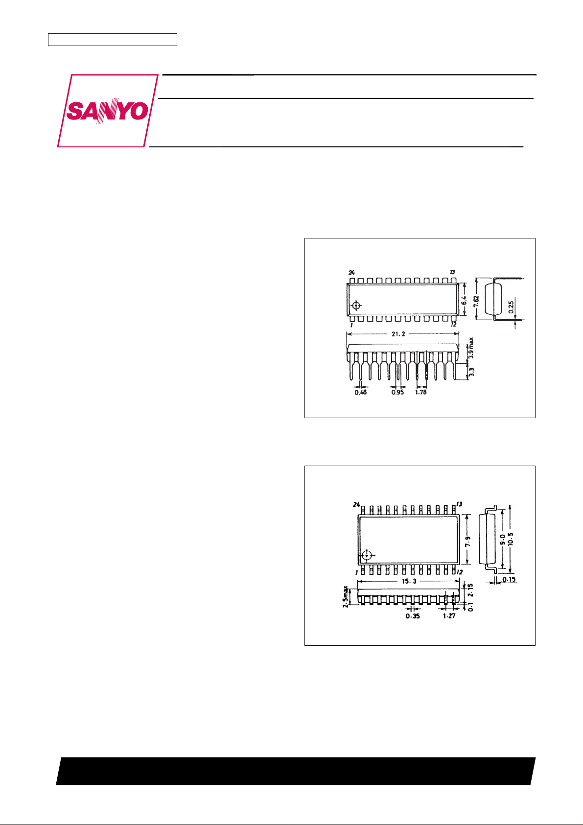
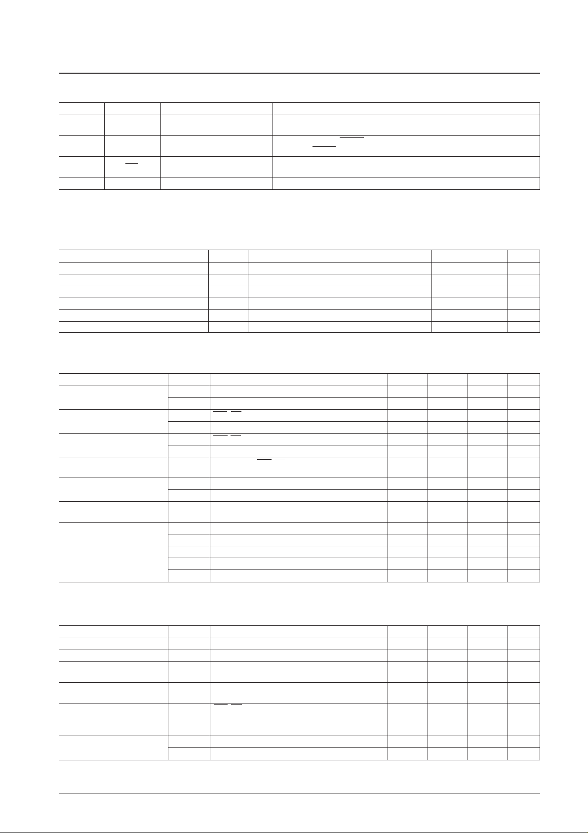
• Packages: 24-pin plastic MFP (375 mil)
24-pin plastic DIP (300 mil)
Package Dimensions
unit: mm
3067-DIP24S
CMOS LSI
Ordering number : EN4841C
63097HA (OT)/41596TH (OT)/83194TH (OT) No. 4841-1/12
SANYO Electric Co.,Ltd. Semiconductor Bussiness Headquarters
TOKYO OFFICE Tokyo Bldg., 1-10, 1 Chome, Ueno, Taito-ku, TOKYO, 110 JAPAN
On-Screen Display Controller
LC74723, 74723M
SANYO: DIP24S
[LC74723]
unit: mm
3045B-MFP24
SANYO: MFP24
[LC74723M]

Pin Assignment
Pin Functions
No. 4841-2/12
LC74723, 74723M
Pin No. Symbol Function Description
1 V
SS
1 Ground Ground (digital system ground)
2 Xtal
IN
Crystal oscillator connection
Used either for connecting the external crystal and capacitor that are used for internal
3 Xtal
OUT
synchronization signal generation, or to input an external clock signal (2fscor 4fsc).
4 CTRL1 Crystal oscillator input switching
Switches the LC74723 between external clock input mode and crystal oscillator mode.
Low = crystal oscillator mode, high = external clock mode
5 CSYN
OUT
Composite synchronization Outputs a composite synchronization signal. Outputs the crystal oscillator clock on
signal output reset, i.e., when RST is low.
6 OSC
IN
LC oscillator
Connections for the coil and capacitor that form the oscillator used to generate the
7 OSC
OUT
character output dot clock.
Outputs the result of judging whether or not there is an external synchronization
8 SYNC
JDG
External synchronization signal signal. Outputs a high level when an external synchronization signal is present.
judgment output Outputs the dot clock (LC oscillator) on reset, i.e., when RST is low. (The LC74723
can be set not to output this signal on reset using control data.)
9 CS Enable input
Enables serial data input. Serial data input is enabled when this input is low. There is
a built-in pull-up resistor on this input (hysteresis input).
10 SCLK Clock input
Inputs the clock signal used for serial data input.
There is a built-in pull-up resistor on this input (hysteresis input).
11 SIN Data input Serial data input. There is a built-in pull-up resistor on this input (hysteresis input).
12 V
DD
2 Power supply
Power supply (analog system power supply) for composite video signal level
adjustment.
13 CV
OUT
Video signal output Composite video signal output
14 NC Must be either connected to ground or left open.
15 CV
IN
Video signal input Composite video signal input
16 V
DD
1 Power supply Power supply (+5 V: digital system power supply)
Video signal input for the built-in sync separator circuit (When the built-in sync
17 SYN
IN
Sync separator circuit input separator circuit is not used, input either the horizontal synchronization signal or the
composite synchronization signal.)
18 SEP
C
Sync separator circuit bias voltage Built-in sync separator circuit bias voltage monitor
19 SEP
OUT
Composite synchronization Outputs the built-in sync separator circuit's composite synchronization signal.
signal output (Outputs the SYN
IN
input signal when the built-in sync separator circuit is not used.)
Inputs the vertical synchronization signal by integrating the output signal from the
20 SEP
IN
Vertical synchronization signal input
SEP
OUT
pin.
An integration circuit must be connected between the SEP
OUT
pin and this pin. Hold
at V
DD
1 if this input is unused.
Continued on next page.
Continued from preceding page.
Note: * Both the VDD1 pins (pins 16 and 24) must be connected.
Specifications
Absolute Maximum Ratings at Ta = 25°C
Allowable Operating Ranges at Ta = –30 to +70°C
Note: When the XtalINpin is used in clock input mode, be extremely careful of input noise.
Electrical Characteristics at Ta = –30 to +70°C, VDD1 = 5 V unless otherwise specified
No. 4841-3/12
LC74723, 74723M
Pin No. Symbol Function Description
21 CTRL2 NTSC/PAL-M switch input
Switches the synchronization signal generation between NTSC and PAL-M.
Low = NTSC, high = PAL-M
22 CTRL3 SEP
IN
input control
Controls whether the VSYNC signal is input to SEP
IN
.
Low = Input VSYNC, high = do not input.
23 RST Reset input
System reset input
There is a built-in pull-up resistor on this input (hysteresis input).
24 V
DD
1 Power supply (+5 V) Power supply (+5 V: digital system power supply)
Parameter Symbol Conditions Ratings Unit
Maximum supply voltage V
DD
max VDD1, VDD2 VSS– 0.3 to VSS+ 7.0 V
Maximum input voltage V
IN
max All input pins VSS– 0.3 to VDD+ 0.3 V
Maximum output voltage V
OUT
max CSYN
OUT
, SYNC
JDG
, SEP
OUT
VSS– 0.3 to VDD+ 0.3 V
Allowable power dissipation Pd max Ta = 25°C 350 mW
Operating temperature Topr –30 to +70 °C
Storage temperature Tstg –40 to +125 °C
Parameter Symbol Conditions min typ max Unit
Supply voltage
V
DD
1 VDD1 4.5 5.0 5.5 V
V
DD
2 VDD2 4.5 5.0 1.27 VDD1 V
Input high level voltage
V
IH
1 RST, CS, SIN, SCLK 0.8 VDD1 VDD1 + 0.3 V
V
IH
2 CTRL1, CTRL2, CTRL3, SEP
IN
0.7 VDD1 VDD1 + 0.3 V
Input low level voltage
V
IL
1 RST, CS, SIN, SCLK VSS– 0.3 0.2 VDD1 V
V
IL
2 CTRL1, CTRL2, CTRL3, SEP
IN
VSS– 0.3 0.3 VDD1 V
Pull-up resistance R
PU
Applies to the RST, CS, SIN, and SCLK pins and to
25 50 90 kΩ
the pins specified by options.
Composite video input voltage
V
IN
1 CVIN; VDD1 = 5 V 2.0 Vp-p
V
IN
2 SYNIN; VDD1 = 5 V 2.0 2.5 Vp-p
Input voltage V
IN
3
Xtal
IN
(when external clock input is used)
0.1 5.0 Vp-p
f
in
= 2fscor 4fsc; VDD1 = 5 V
f
osc
1 XtalINand Xtal
OUT
oscillator pins (2fsc: NTSC) 7.159 MHz
f
osc
1 XtalINand Xtal
OUT
oscillator pins (4fsc: NTSC) 14.318 MHz
Oscillator frequency f
osc
1 XtalINand Xtal
OUT
oscillator pins (2fsc: PAL-M) 7.151 MHz
f
osc
1 XtalINand Xtal
OUT
oscillator pins (4fsc: PAL-M) 14.302 MHz
f
osc
2 OSCINand OSC
OUT
oscillator pins (LC oscillator) 5 12 MHz
Parameter Symbol Conditions min typ max Unit
Input off leakage current I
leak
1 CV
IN
1 µA
Output off leakage current I
leak
2 CV
OUT
1 µA
Output high level voltage V
OH
1
CSYN
OUT
, SYNC
JDG
, SEP
OUT
;
3.5 V
V
DD
1 = 4.5 V, IOH= –1.0 mA
Output low level voltage V
OL
1
CSYN
OUT
, SYNC
JDG
, SEP
OUT
;
1.0 V
V
DD
1 = 4.5 V, IOL= 1.0 mA
I
IH
RST, CS, SIN, SCLK, CTRL1, CTRL2, CTRL3, SEPIN;
1 µA
Input current
V
IN
= VDD1
I
IL
CTRL1, CTRL2, CTRL3, OSCIN; VIN= VSS1 –1 µA
Current drain (operating)
I
DD
1 VDD1; All outputs open, Xtal: 7.159 MHz, LC: 8 MHz 15 mA
I
DD
2 VDD2; VDD2 = 5 V 20 mA
Continued on next page.

Continued from preceding page.
Timing Characteristics at Ta = –30 to +70°C, VDD1 = 5 ± 0.5 V
Serial Data Input Timing
No. 4841-4/12
LC74723, 74723M
Parameter Symbol Conditions min typ max Unit
Sync level V
SN
When the sync level is 0.8 V, CV
OUT
: VDD1, VDD2 = 5 V 0.69 0.81 0.93 V
When the sync level is 1.0 V, CV
OUT
: VDD1, VDD2 = 5 V 0.89 1.01 1.13 V
Pedestal level V
PD
When the sync level is 0.8 V, CV
OUT
: VDD1, VDD2 = 5 V 1.28 1.40 1.52 V
When the sync level is 1.0 V, CV
OUT
: VDD1, VDD2 = 5 V 1.47 1.59 1.71 V
Color burst low level V
CBL
When the sync level is 0.8 V, CV
OUT
: VDD1, VDD2 = 5 V 0.97 1.09 1.21 V
When the sync level is 1.0 V, CV
OUT
: VDD1, VDD2 = 5 V 1.16 1.28 1.40 V
Color burst high level V
CBH
When the sync level is 0.8 V, CV
OUT
: VDD1, VDD2 = 5 V 1.60 1.72 1.84 V
When the sync level is 1.0 V, CV
OUT
: VDD1, VDD2 = 5 V 1.79 1.91 2.03 V
Background color low level V
RSL
When the sync level is 0.8 V, CV
OUT
: VDD1, VDD2 = 5 V 1.44 1.56 1.68 V
When the sync level is 1.0 V, CV
OUT
: VDD1, VDD2 = 5 V 1.63 1.75 1.87 V
Background color high level V
RSH
When the sync level is 0.8 V, CV
OUT
: VDD1, VDD2 = 5 V 1.96 2.08 2.20 V
When the sync level is 1.0 V, CV
OUT
: VDD1, VDD2 = 5 V 2.16 2.28 2.40 V
Trimming level 0 V
BK0
When the sync level is 0.8 V, CV
OUT
: VDD1, VDD2 = 5 V 1.43 1.55 1.67 V
When the sync level is 1.0 V, CV
OUT
: VDD1, VDD2 = 5 V 1.61 1.73 1.85 V
Trimming level 1 V
BK1
When the sync level is 0.8 V, CV
OUT
: VDD1, VDD2 = 5 V 2.01 2.13 2.25 V
When the sync level is 1.0 V, CV
OUT
: VDD1, VDD2 = 5 V 2.18 2.30 2.42 V
Character level V
CHA
When the sync level is 0.8 V, CV
OUT
: VDD1, VDD2 = 5 V 2.57 2.69 2.81 V
When the sync level is 1.0 V, CV
OUT
: VDD1, VDD2 = 5 V 2.76 2.88 3.00 V
Parameter Symbol Conditions min typ max Unit
Minimum input pulse width
t
W (SCLK)
SCLK 200 ns
t
W (CS)
CS (the period while CS is high) 1 µs
Data setup time
t
SU (CS)
CS 200 ns
t
SU (SIN)
SIN 200 ns
Data hold time
t
h (CS)
CS 2 µs
t
h (SIN)
SIN 200 ns
One word write time
t
word
The time to write 8 bits of data 4.2 µs
t
wt
The RAM data write time 1 µs
 Loading...