

Sanyo LC7471 Specifications

Any and all SANYO products described or contained herein do not have specifications that can handle
applications that require extremely high levels of reliability, such as life-support systems, aircraft’s
control systems, or other applications whose failure can be reasonably expected to result in serious
physical and/or material damage. Consult with your SANYO representative nearest you before using
any SANYO products described or contained herein in such applications.
SANYO assumes no responsibility for equipment failures that result from using products at values that
exceed, even momentarily, rated values (such as maximum ratings, operating condition ranges,or other
parameters) listed in products specifications of any and all SANYO products described or contained
herein.
CMOS IC
On-Screen Display Controller
for NTSC-Format Video
Ordering number:ENN
*
4088
LC7471
SANYO Electric Co.,Ltd. Semiconductor Company
TOKYO OFFICE Tokyo Bldg., 1-10, 1 Chome, Ueno, Taito-ku, TOKYO, 110-8534 JAPAN
81001TN (KT)/5182JN(US) No.4088–1/12
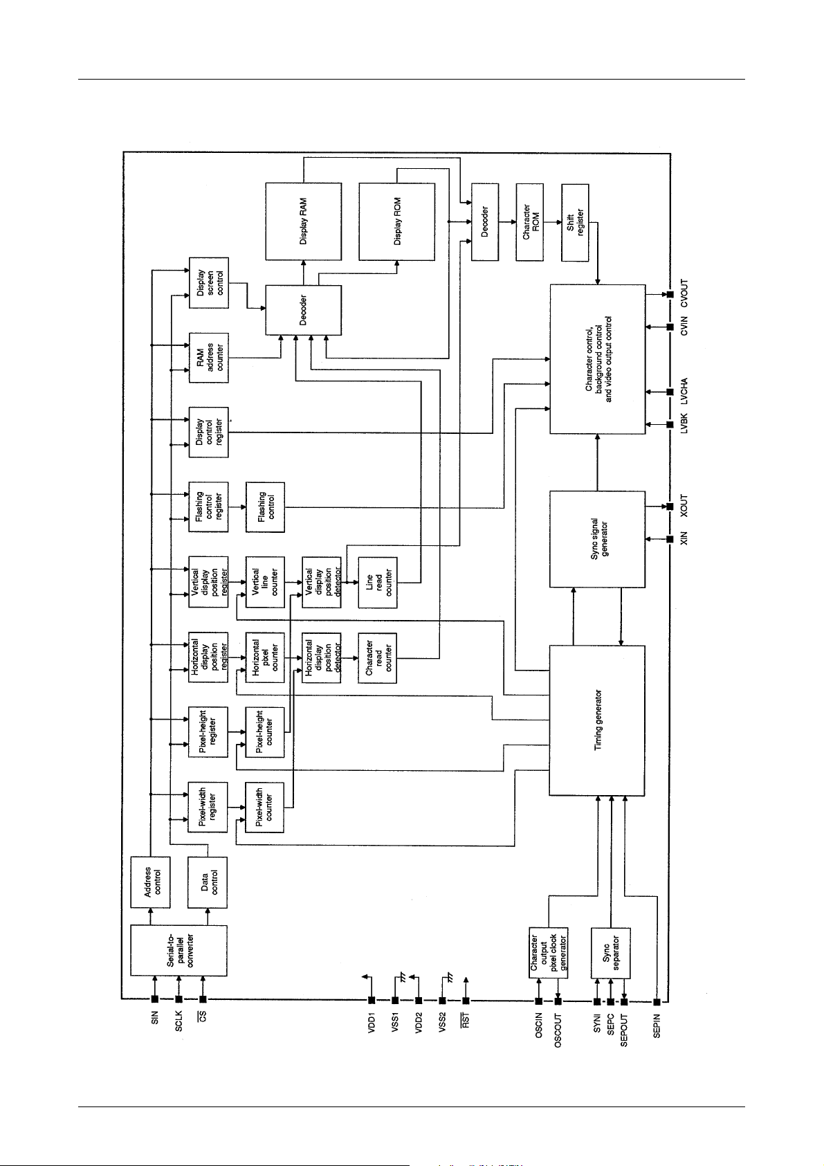
Overview
The LC7471 is a video display controller for superimpos-
ing text and low-level graphics onto an NTSC-format tele-
vision receiver. The LC7471 incorporates a 64 character
internal character generator ROM, a 24-character × 64-line
display ROM and a 176-character display RAM. Up to 288,
12 × 18-pixel characters can be displayed under micropro-
cessor control on a 24-character by 12-line display.
The LC7471 features selectable pixel width and pixel
height, and 64 vertical and 64 horizontal display start posi-
tions. It also features a flashing enable bit for each charac-
ter position.
The LC7471 operates from a 5 V supply and is a v ailable in
22-pin shrink DIPs.
Features
• Complete text and graphics video overlay circuitry.
• 64-character internal character generator ROM.
• 24-character × 64-line display ROM.
• 176-character display RAM.
• 288-character display capability.
• 12 × 18-pixel characters.
• Four pixel widths.
• Four pixel heights.
• Selectable background color.
• Approximately 0.5 or 1 s period character flashing op-
tion.
• 25, 50 or 75% flashing duty cycle.
• Internal or external synchronization.
• Serial data control.
• 5 V supply.
• 22-pin shrink DIP.
21.2
0.95 0.48
1.7
1.78
3.9max
0.51min
6.4
7.62
3.3
3.25
0.25
111
22 12
Package Dimensions
unit:mm
3059-DIP22S
[LC7471]
SANYO : DIP22S
Pin Assignment
Preliminary
Top view
LC7471
No.4088–2/12
Block Diagram
LC7471
No.4088–3/12
retemaraPlobmySsnoitidnoCsgnitaRtinU
egatlovylppuSV
DD
V
SS
–Vot3.0
SS
0.7+
V
egatlovtupnIV
I
V
SS
–Vot3.0
DD
3.0+
V
egatlovtuptuOV
O
V
SS
–Vot3.0
DD
3.0+
V
noitapissidrewopelbawollAxamdP 003Wm
erutarepmetgnitarepOrpoT –07+ot03
erutarepmetegarotSgtsT –521+ot04
Reommended Operating Conditions at Ta = 25˚C
Specifications
Absolute Maximum Ratings
˚C
˚C
Pin Description
rebmuNemaNnoitpircseD
1V
1SS
dnuorgtiucriclatigiD
2NIXtupnirotallicsolatsyrC
3TUOXtuptuorotallicsolatsyrC
4TSETtuptuotseT
5TSRsiseretsyhhtiwtupniteserWOL-evitcA
6KLCSsiseretsyhhtiwtupnikcolcatadlaireS
7NISsiseretsyhhtiwtupniatadlaireS
8SCsiseretsyhhtiwtupnitcelespihcWOL-evitcA
9KBVLtupnitnemtsujdalevel-gniknalB
01AHCVLtupnitnemtsujdalevel-retcarahC
11V
2DD
ylppustiucricgolanA
21TUOVCtuptuooedivetisopmoC
31V
2SS
dnuorgtiucricgolanA
41NIVCtupnioedivetisopmoC
51V
1DD
ylppuscigolV5
61INYStupnirotarapescnyS
71CPESnoitcennocroticapacrotarapescnyS
81TUOPEStuptuorotarapescnyS
91NIPEStupnicnyslacitreV
02TUOCSO
snoitcennockrowtenrotallicsoCLkcolc-lexiP
12NICSO
22V
1DD
ylppuscigolV5
retemaraPlobmySsnoitidnoCsgnitaRtinU
egatlovylppuscigoLV
1DD
5V
egatlovylppusgolanAV
2DD
5V
egnaregatlovylppuscigoLV
1DD
5.5ot5.4V
egnaregatlovylppusgolanAV
2DD
V72.1ot5.4
1DD
V
Ta = 25˚C
Electrical Characteristics at Ta = –30 to +70˚C, V
DD1
= 5V, unless otherwise noted
retemaraPlobmySsnoitidnoC
sgnitaR
tinU
nimpytxam
tnerrucylppuSI
DD
V
TSR
V=
1DD
f,
LATX
f,zHM13.41=
CL
,zHM7=
V
2DD
nepoerastuptuolladna
51Am
tupnilevel-WOLKLCSdnaTSR,NIS,SC
egatlov
V
LI
V
SS
–3.0V2.0
1DD
V
tupnilevel-HGIHKLCSdnaTSR,NIS,SC
egatlov
V
HI
V8.0
1DD
V
1DD
3.0+
V
egatlovtupnioedivetisopmocINYSV
1NI
0.25.2V
P-P
egatlovtupnioedivetisopmocNIVCV
2NI
2V
P-P
tnerructupnilevel-WOLNICSOV
LI
V
I
V=
SS
–1 Aµ
level-HGIHNIPESdnaKLCS,TSR,NIS,SC
tnerructupni
V
HI
V
I
V=
DD
1Aµ
egatlovtuptuolevel-WOLTUOPESV
LO
V
1DD
I,V5.4=
LO
Am1=0.1V
egatlovtuptuolevel-HGIHTUOPESV
HO
V
1DD
I,V5.4=
HO
Am1=5.3V
ycneuqerfrotallicsOf
CSO
f
LATX
f4=
CS
813.41
zHMf
LATX
f2=
CS
951.7
rotallicsoCL5701
tnerrucegakaelTUOVCI
L
01Aµ

LC7471
No.4088–4/12
Timing Characteristics at Ta = –30 to +75˚C, V
DD1
= 5±0.5V
retemaraPlobmySsnoitidnoC
sgnitaR
tinU
nimpytxam
htdiwesluptupniKLCSt
)KLCS(W
002sn
htdiwesluptupnilevel-HGIHSCt
)SC(W
1sµ
emitputestupnielbaneatadSCt
)SC(US
002sn
emitputestupniatadNISt
)NIS(US
002sn
emitdlohtupnielbaneatadSCt
)SC(H
2sµ
emitdlohtupniatadNISt
)NIS(H
002sn
emitetirwdrowatadtib-61t
drow
01sµ
emitetirwatadMARt
TW
1sµ
Input Timing
Data and address words are input in serial format on SIN.
A 16-bit address word followed by 16-bit data words is
input after the falling edge of CS. The address automati-
cally increments after each data word. The data input tim-
ing is shown in the following figure.
Only the lower eight bits of the address word are signifi-
cant. Only the lower eight bits of data words at addresses
000H to 0AFH, the lower 11 bits of data words at
addresses 0B0H to 0BBH and the lower 12 bits of data
words at addresses 0BCH to 0BFH are significant. All
non-significant bits should be set to 0.
 Loading...