


Ordering number: EN2119D
CMOS LSI
LC7461M
Infrared Remote Control Transmitter IC
Functions
.
32%3 function keys
.
13-bit custom codes
.
Operating supply voltage range VDD= 1.8 to 3.6 V
.
Supply current at the standby mode IDD= 1 µA or less
.
Double-press operation keys (no priority given)
.
On-chip oscillator (ceramic resonator : connected externally)
Package Dimensions
unit : mm
3045B-MFP24
[LC7461M]
Features
.
The custom code consists of 7 bits to be fixed by the
on-chip ROM and 6 bits being pin-settable. Sixty-four
custom codes may be selected externally (no diode required).
.
Minimum number of external parts required
SANYO : MFP24
Specifications
Absolute Maximum Ratings at Ta = 25°C
Parameter Symbol Conditions Ratings Unit
Maximum supply voltage V
Input voltage V
Output voltage V
Output current I
Allowable power dissipation Pd max Ta % 85°C 150 mW
Operating temperature Topr –40 to +85 °C
Storage temperature Tstg –50 to +125 °C
max V
DD
IN
OUT
OUT
DD
Each input pin VSS–0.3 to VDD+0.3 V
Each output pin VSS–0.3 to VDD+0.3 V
OUT –35 mA
VSS–0.3 to +5.5 V
Allowable Operating Conditions at Ta = 25°C
Parameter Symbol Pin Name Conditions min typ max Unit
Supply voltage V
Input high-level voltage V
Input low-level voltage V
Oscillation frequency f
DD
IH
IL
OSC
V
DD
KI0toKI3,
C
to C
0
KI0toKI3,
C
to C
0
f
= 455 kHz 1.8 3.0 3.6 V
OSC
0.7 V
5
5
DD
V
SS
400 455 500 kHz
SANYO Electric Co.,Ltd. Semiconductor Bussiness Headquarters
TOKYO OFFICE Tokyo Bldg., 1-10, 1 Chome, Ueno, Taito-ku, TOKYO, 110 JAPAN
O3096HA(II)/7058YT/6036KI,TS(KOTO) No.2119-1/7
0.3V
V
DD
DD
V
V

LC7461M
Electrical Characteristics at Ta = 25°C, VDD= 3.0 V
Parameter Symbol Pin Name Conditions min typ max Unit
Operating supply
current
Quiescent supply
current
Output high-level
current
Output high-level
voltage
Output low-level
voltage
Output OFF-state
leakage current
Input high-level current I
Input low-level current I
Input floating voltage V
Input pull down
resistance
Internal Block Diagram
I
DD
I
DS
I
1 OUT VDD= 1.8 V, VOH= 1.0 V –8 mA
OH
I
2 OUT VDD= 3.0 V, VOH= 1.0 V –25 mA
OH
V
OH
V
OL
I
OFF
IH
IL
IF
R
IN
V
DD
V
DD
KO0toKO7IOH= –0.1 mA 0.3 V
OUT IOL= 0.1 mA 0.3 V
KO0toKO71µA
C0to C
C0to C
KI0toKI3 0.1 V
KI0toKI3 75 100 125 kΩ
Key ON, output: no load 1 mA
All keys OFF, OSC stop 1 µA
VIN=V
5
5
VIN=V
DD
SS
–1 µA
1µA
V
DD
Key
output
timing
signal
generator
Oscillator
Key
entry
circuit
Divider
Key data
register
Output
circuit
Decoder
Custom code
register
No.2119-2/7
LC7461M
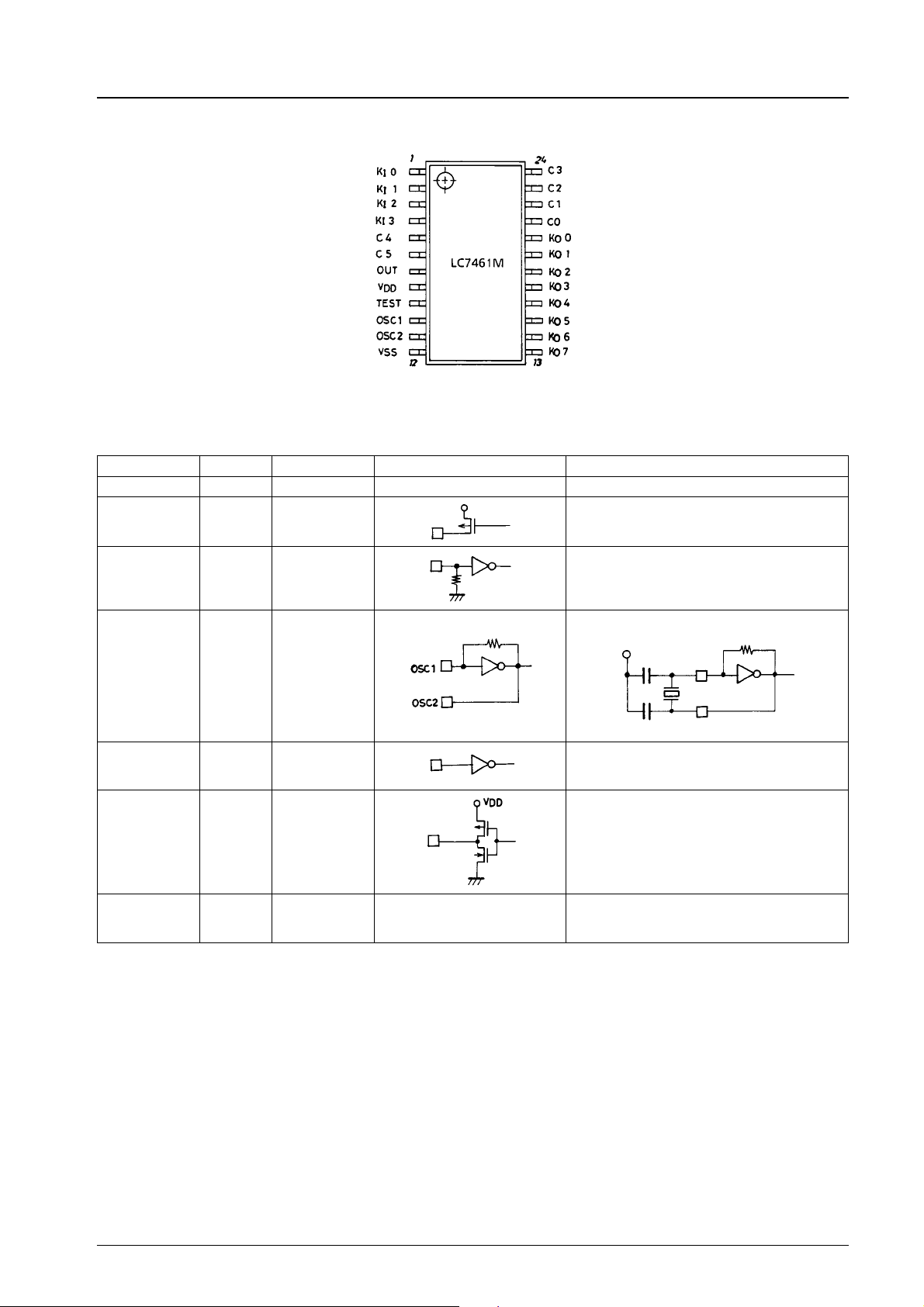
Pin Assignment
Top view
Pin Description
Pin Name Pin No. Input/Output Internal Equivalent Circuit Pin Function
V
DD,VSS
0toKO7 13 to 20 Output Key scan timing signal output pins
K
O
8, 12 Power supply pins VSS= GND
K
0toKI3 1 to 4 Input Keys return signal entry pins
I
Input/output pins for ceramic resonator-used
oscillation
OSC1
OSC2
C
to C
0
5
OUT 7 Output
TEST 9 Input
10
11
21 to 24,
5, 6
Input/output
Input
Oscillator configuration
Input pins for custom code setting
Capable of externally setting 6 bits of 13 bits in
all that provide a custom code
Output pin for transmit LED drive
LSI test pin
Normally set to high-level or brought to open
state
No.2119-3/7
 Loading...