

Ordering number : EN5680
D3097HA(OT) No. 5680-1/13
Overview
The LC7455A/M extracts the closed caption signal
superimposed on a video signal during the vertical return
period and, under the control of a clock signal provided by
the decoder IC, transfers that signal to the IC (usually a
microcontroller) that decodes the closed caption data. The
LC7455A/M supports four operating modes. Modes 1 and
2 can be used for XDS. In these modes, the LC7455A/M,
in combination with the decoder IC (microcontroller),
extracts the caption signal superimposed on field 2 and
uses it for NTSC VCR functions such as the automatic
time and date setting function. In modes 3 and 4, the
LC7455A/M, in combination with the decoder IC
(microcontroller), extracts the caption signal
superimposed on fields 1 and 2 and uses it for NTSC TV
applications (mode 3) or PAL TV applications (mode 4).
Functions
• Low power dissipation achieved by fabrication in a
CMOS process.
• Stable caption signal extraction achieved by a built-in
peak hold circuit and the use of digital technology.
• Operating supply voltage: 5 V ±10%
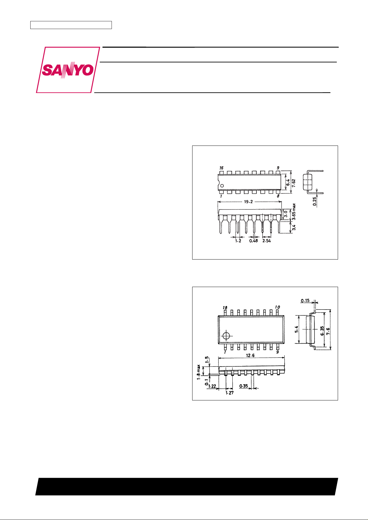
• Package LC7455A: 16-pin DIP
LC7455M: 18-pin MFP
Package Dimensions
unit: mm
3006B-DIP16
unit: mm
3095-MFP18
SANYO: DIP16
[LC7455A]
SANYO: MFP18
[LC7455M]
LC7455A, 7455M
SANYO Electric Co.,Ltd. Semiconductor Bussiness Headquarters
TOKYO OFFICE Tokyo Bldg., 1-10, 1 Chome, Ueno, Taito-ku, TOKYO, 110 JAPAN
Closed Caption Signal Extraction IC
CMOS IC
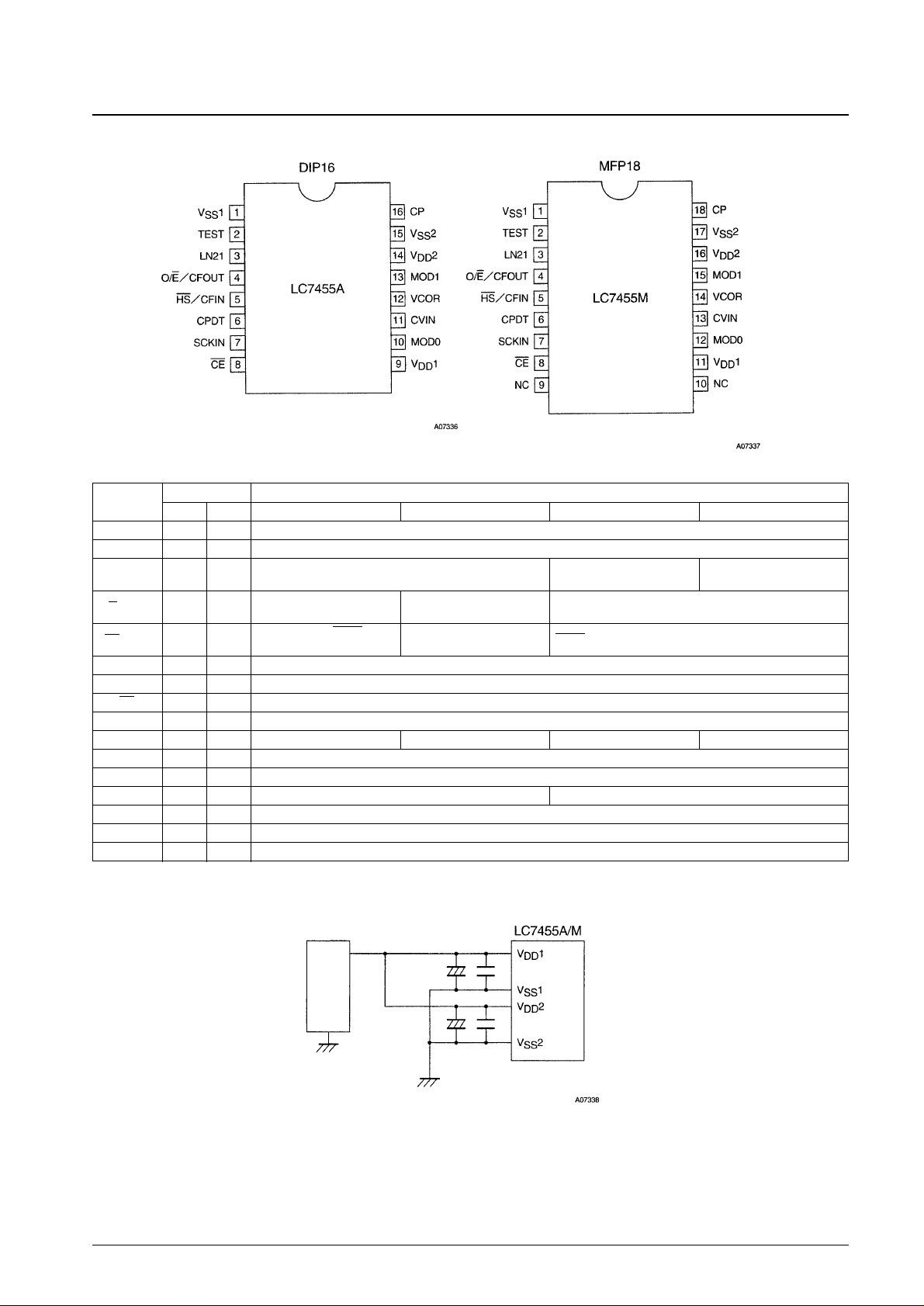
Pin Assignments
Note: VDD1 and VSS1 are the power supply for the digital block, and VDD2 and VSS2 are the power supply for the analog block. Use a circuit similar to the
one shown below to minimize mutual interference due to noise from these blocks.
No. 5680-2/13
LC7455A, 7455M
Pin Functions
Pin
Pin No. Pin function
DIP16 MFP18 Mode 1 Mode2 Mode3 Mode4
V
SS
1 1 1 Ground
TEST 2 2 Test pin. Must be left open during normal operation.
LN21 3 3 Line 21H pulse output (even field)
Line 21H pulse output Line 22H pulse output
(both fields) (both fields)
O/E/CFOUT 4 4
Field discrimination pulse
Ceramic oscillator output Field discrimination pulse output
output
HS/CFIN 5 5
Sync separator Hsync
Ceramic oscillator input Hsync pulse input
pulse output
CPDT 6 6 Caption data output (n-channel open-drain output)
SCKIN 7 7 Caption data transfer clock input
CE 8 8 Chip select input
V
DD
1 9 11 Power supply
MOD0 10 12 Leave open Short to the power supply Leave open Short to the power supply
CVIN 11 13 Composite video input
VCOR 12 14 Connection for an external resistor to control the built-in VCO oscillator frequency
MOD1 13 15 Leave open Short to the power supply
V
DD
2 14 16 Power supply
V
SS
2 15 17 Ground
CP 16 18 Connection for the filter used by the built-in PLL
Power
supply
Top view
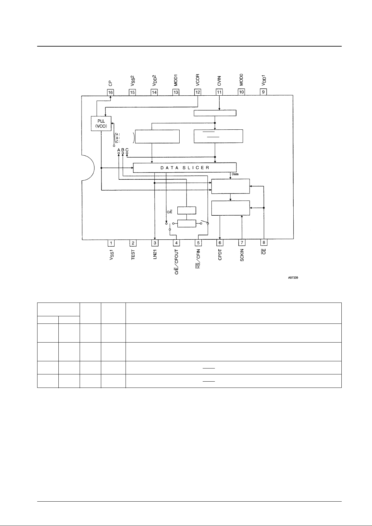
System Block Diagram
No. 5680-3/13
LC7455A, 7455M
Operation in the Different Modes
Pin Application
Mode
equipment
Operation
MOD1 MOD0
· Even field line 21 data extraction
Open Open Mode 1 VCR The internal PLL is operated with the horizontal synchronizing signal separated from the composite video
signal as the reference.
· Even field line 21 data extraction
Open V
DD
Mode 2 VCR An external 508 kHz ceramic oscillator is used, and the internal PLL is operated with that oscillator output
divided by 32 as the reference.
V
DD
Open Mode 3 NTSC-TV
· Odd and even field line 21 data extraction
The internal PLL is operated with the Hsync signal applied from fly back as the reference.
V
DD
V
DD
Mode 4 PAL-TV
· Odd and even field line 22 data extraction
The internal PLL is operated with the Hsync signal applied from the fly back circuit as the reference.
Note: The data extraction operations in modes 1 and 2 are identical. However, while mode 1 can operate without problem for normal "on air" signals, it may
be difficult for the PLL to lock with signals such as scrambled CATV signals.
PLL reference clock
mode 2
mode 3, 4
mode 1
Data peak hold
(Data slice)
Hsync peak hold
(Hsync slice)
Output control
Data output
buffer
Divided-by-
32 circuit
Oscillator
circuit
Pedestal clamp
(Mode 2)
(Mode 2)
(Modes 1, 3, 4)
No. 5680-4/13
LC7455A, 7455M
Parameter Symbol Conditions Ratings Unit
Maximum supply voltage V
DD
max VDD1, VDD2: VDD1 = VDD2 –0.3 to +7.0 V
Input voltage V
I
HS/CFIN, CVIN, SCKIN, CE –0.3 to VDD+0.3 V
Output voltage V
O
LN21, CPDT, O/E/CFOUT, HS/CFIN –0.3 to VDD+0.3 V
Allowable power dissipation Pd max
LC7455A 300 mW
LC7455M 150 mW
Operating temperature Topr –30 to +70 °C
Storage temperature Tstg –55 to +150 °C
Specifications
Absolute Maximum Ratings at Ta = 25°C, VSS= 0 V
Note: VSS1 and VSS2 must be at the same potential.
V
DD
1 and VDD2 must be at the same potential.
Parameter Symbol Conditions
Ratings
Unit
min typ max
Operating supply voltage V
DDVDD
1, VDD2 : VDD1 = VDD2 4.5 5.5 V
Input high-level voltage V
IH
HS/CFIN, SCKIN, CE;
0.75 V
DD
V
DD
V
V
DD
= 4.5 to 5.5 V
Input low-level voltage V
IL
HS/CFIN, SCKIN, CE;
V
SS
0.25V
DD
V
V
DD
= 4.5 to 5.5 V
CVIN input amplitude CVSYNC
CVIN : SYNC-WHITE = 1.0 V;
1Vp-p – 3dB
1Vp-p
1Vp-p + 3 dB
V
V
DD
= 4.5 to 5.5 V
HS/CFIN : V
DD
= 4.5 V
HS input frequency range f
H
For mode 3 15.23 15.73 16.23 kHz
For mode 4 15.13 15.63 16.13 kHz
HS/CFIN, O/E/CFOUT;
Oscillator frequency range*
1
FmCF For mode 2, see Figure 1. 503 508 513 kHz
VDD= 4.5 to 5.5 V
HS/CFIN, O/E/CFOUT;
Oscillator stabilization time*
2
tmsCF For mode 2, see Figure 2. 0.5 5 ms
VDD= 4.5 to 5.5 V
Allowable Operating Ranges at Ta = –30 to +70°C, VSS= 0 V
Parameter Symbol Conditions
Ratings
Unit
min typ max
Input high-level current I
IH
HS/CFIN, SCKIN, CE : VIN= VDD; 1 µA
V
DD
= 4.5 to 5.5 V
Input low-level current I
IL
HS/CFIN, SCKIN, CE : VIN= VSS; –1 µA
V
DD
= 4.5 to 5.5 V
Output high-level voltage V
OH
LN21, O/E/CFOUT, HS/CFIN;
V
DD
– 1.2 V
I
OH
= –4 mA ; VDD= 4.5 to 5.5 V
Output low-level voltage V
OL
LN21, CPDT, O/E/CFOUT, 1 V
HS/CFIN : I
OL
= 10 mA; VDD= 4.5 to 5.5 V
Input clamping voltage V
CLMP
CVIN ; VDD= 5.0 V 2.3 2.5 2.7 V
Input clamping current I
IC
CVIN : CVIN = 3 V ; VDD= 5.0 V 5 10 18 µA
Output clamping current I
OC
CVIN : CVIN = 2 V ; VDD= 5.0 V –120 –70 –30 µA
Current drain I
DD
VDD1, VDD2 ; VDD= 4.5 to 5.5 V 6 15 mA
Electrical Characteristics at Ta = –30 to +70°C, VSS= 0 V.
Note: 1. See Table 1 for more information on the oscillator frequency.
2. The oscillator stabilization time is the time required until the oscillator is stable after the power-supply voltage is applied. See figure 2.
Parameter Symbol Conditions
Ratings
Unit
min typ max
[Serial clock]
Input clock period t
CKCY
SCKIN : See Figure 3. 1 µs
Input clock low-level pulse width t
CKL
SCKIN : See Figure 3. 0.5 µs
Input clock high-level pulse width t
CKH
SCKIN : See Figure 3. 0.5 µs
Setup time t
ICK
SCKIN : Stipulated with respect to the falling
1 µs
edge of CE.
[Serial output]
Output delay time t
CKO
0.5 µs
Serial Output Characteristics at Ta = –30 to +70°C, VSS= 0 V, VDD= 4.5 to 5.5 V
Stipulated with respect to the falling edge of
SCKIN. A 1-kΩ external pull-up resistor is
connected. See Figure 3.

No. 5680-5/13
LC7455A, 7455M
Table 1 Ceramic Oscillator Guaranteed Constants
Figure 1 Ceramic Oscillator
Figure 2 Oscillator Stabilization Time
Figure 3 Serial Output Test Conditions
Note: Capacitors with K tolerance (±10%) and SL characteristics must be used for C1 and C2.
· Since this circuit is influenced by the length of the circuit pattern, components related to oscillator functioning must be mounted as close together as
possible so that pattern lines do not become longer than is absolutely necessary.
· The characteristics are not guaranteed if an oscillator element other than the one listed above is used.
Oscillator type Manufacturer Oscillator element C1 C2
508-kHz ceramic oscillator Murata Mfg. Co., Ltd. CSB 508E 150 pF 150 pF
Power supply
Operating V
DD
lower limit
<AC timing measurement point>
<Timing>
<Test load>
Note: CPDT goes to the high-impedance state while CE is high.

O/E and LN21 Output Timing (Modes 1, 2, and 3)
No. 5680-6/13
LC7455A, 7455M
Notes: O/E is output in modes 1 and 3. In mode 2 it functions as the ceramic oscillator output pin.
LN21 is output for even fields in modes 1 and 2, and for both fields in mode 3.
Line no.
Line no.
(modes 1, 3)
(modes 1, 3)
Odd field
Even field
This pulse is only output in mode 3.
This pulse is only output in modes 1, 2, and 3.

No. 5680-7/13
LC7455A, 7455M
O/E and LN21 Output Timing (Mode 4)
Line no.
Line no.
First field
Second field

No. 5680-8/13
LC7455A, 7455M
Caption Data Transfer from the LC7455A/M to the Decoder IC (microcontroller): Method 1
(This is the basic technique.)
Notes: Applications that extract closed caption text data in mode 3 (NTSC TV) or mode 4 (PAL TV) must check the level of the O/E/CFOUT pin when an
LN21 falling edge is detected to determine whether odd field or even field data is being acquired.
(Caption data is transferred to the data output buffer.)
In modes 1 and 2, pulses are output on line 21 of even fields.
In mode 3, pulses are output on line 21 of both fields.
In mode 4, pulses are output on line 22 of both fields.
(
)
(The decoder IC (microprocessor) sets CE from high to low after detecting a falling edge on LN21.)
High impedance
The previous data is output.
(Sixteen bits of caption data is output LSB first in synchronization with falling edges on SCKIN.)

Caption Data Transfer from the LC7455A/M to the Decoder IC (microcontroller): Method 2
(For applications that cannot provide an input port on the decoder IC (microcontroller) to detect LN21 falling edges.)
No. 5680-9/13
LC7455A, 7455M
In modes 1 and 2, since data is output to the output buffer once every frame (in the even field), the decoder IC (microcontroller) must perform a transfer control operation at least twice every frame (about 32 ms).
When the second control operation is performed in a given frame, the CPDT output for that second operation will be 16 bits of zeros. This allows the microprocessor to recognize that the data for the next frame has not yet been
transferred to the output buffer.
Notes: When CE remains low, the hardware will not transfer the data to the output buffer. Thus applications must restore CE from low to high after each data transfer to the decoder IC (microcontroller) operation has completed.
This transfer technique (method 2) cannot be used in modes 3 and 4.
Within a single frame (modes 1 and 2)
16 bits of data all
of which are zeros.
16 bits transfered

Sample Application Circuits (mode 1)
MFP18
DIP16
No. 5680-10/13
LC7455A, 7455M

No. 5680-11/13
LC7455A, 7455M
Sample Application Circuits (mode 2)
MFP18
DIP16

No. 5680-12/13
LC7455A, 7455M
Sample Application Circuits (mode 3)
MFP18
DIP16
Hsync signal
Hsync signal

No. 5680-13/13
LC7455A, 7455M
This catalog provides information as of December, 1997. Specifications and information herein are subject to
change without notice.
■ No products described or contained herein are intended for use in surgical implants, life-support systems, aerospace
equipment, nuclear power control systems, vehicles, disaster/crime-prevention equipment and the like, the failure of
which may directly or indirectly cause injury, death or property loss.
■ Anyone purchasing any products described or contained herein for an above-mentioned use shall:
➀ Accept full responsibility and indemnify and defend SANYO ELECTRIC CO., LTD., its affiliates, subsidiaries and
distributors and all their officers and employees, jointly and severally, against any and all claims and litigation and all
damages, cost and expenses associated with such use:
➁ Not impose any responsibility for any fault or negligence which may be cited in any such claim or litigation on
SANYO ELECTRIC CO., LTD., its affiliates, subsidiaries and distributors or any of their officers and employees
jointly or severally.
■ Information (including circuit diagrams and circuit parameters) herein is for example only; it is not guaranteed for
volume production. SANYO believes information herein is accurate and reliable, but no guarantees are made or implied
regarding its use or any infringements of intellectual property rights or other rights of third parties.
Sample Application Circuits (mode 4)
MFP18
DIP16
Hsync signal
Hsync signal
 Loading...