

Page 1
Any and all SANYO products described or contained herein do not have specifications that can handle
applications that require extremely high levels of reliability, such as life-support systems, aircraft’s
control systems, or other applications whose failure can be reasonably expected to result in serious
physical and/or material damage. Consult with your SANYO representative nearest you before using
any SANYO products described or contained herein in such applications.
SANYO assumes no responsibility for equipment failures that result from using products at values that
exceed, even momentarily, rated values (such as maximum ratings, operating condition ranges,or other
parameters) listed in products specifications of any and all SANYO products described or contained
herein.
CMOS IC
DTMF/PULSE Switchable Dialer
Ordering number:ENN3095A
LC7367J, 7367JM
SANYO Electric Co.,Ltd. Semiconductor Company
TOKYO OFFICE Tokyo Bldg., 1-10, 1 Chome, Ueno, Taito-ku, TOKYO, 110-8534 JAPAN
Overview
The LC7367J, 7367JM are DTMF/OUTPUT-PULSE dialer CMOS ICs with redial function for use in pushbutton
telephones.
Features
• Low voltage CMOS process for direct operation from telephone line.
• Possible to use single contact or standard 2-of-7, 2-of-8
key pad.
• Possible to use color-burst crystal resonator for on-chip
oscillator (f
• Possible to use either mode select pin (P/T) or function
key (4×4 matrix key) to select DTMF mode/OUTPUTPULSE mode.
• Mode change with MC key is made in one direction onlyfrom pulse mode to tone mode.
• Delivers 12 DTMF signals when in DTMF mode.
• On-chip 31-digit redial memory.
• Possible to provide mix redial (31 digits-PAUSE-MC) of
DTMF/OUTPUT-PULSE mode.
• Either auto pause select (4s.×n) or manual release available for mode select standby time during redial operation.
• Output pulse make rate of OUTPUT-PULSE mode : Pinselectable (33.2% or 40%).
• Output pulse rate of OUTPUT-PULSE mode : Pinselelctable (10pps or 20pps).
• On-chip circuit to prevent malfunction due to noise pulse
caused by key entry.
• Key touch tone (pacifier tone) output capability.
OUTPUT-PULSE mode : 1243Hz/50ms
• Supply voltage / operating temperature
DTMF mode :
VDD=2.0 to 6.0V / Ta=–30 to +70°C
OUTPUT-PULSE mode :
VDD=1.5 to 6.0V / Ta=–30 to +70°C
=3.58MHz).
OSC
• Operating current
DTMF mode :
IDD=1.0mA max / VDD=3.5V
OUTPUT-PULSE mode :
IDD=500µA max / VDD=3.5V
Continued on next page.
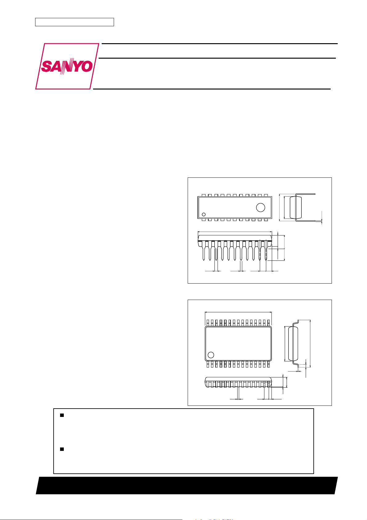
Package Dimensions
unit:mm
3059-DIP22S
[LC7367J]
22 12
6.4
7.62
111
0.95 0.48
unit:mm
3073A-MFP30
30
1
21.2
15.2
0.4
1.78
[LC7367JM]
16
15
1.0
1.7
(0.6)
3.25
3.9max
3.3
0.51min
7.9
(2.25)
0.1
0.25
SANYO : DIP22S
2.45max
SANYO : MFP30
9.2
0.65
0.25
10.5
51001TN (KT)/D1694TH/2280TA, TS (AF) No.3095–1/12
Page 2
Continued from preceding page.
• Data retention current
IDR≤0.5µA / VDD=1.0V
• Package
LC7367J : Dual-in-line shrink 22-pin package
LC7367JM : Miniflat 30-pin package
Pin Assignment
LC7367J, 7367JM
Equivalent Circuit Block Diagram
No.3095–2/12
Page 3
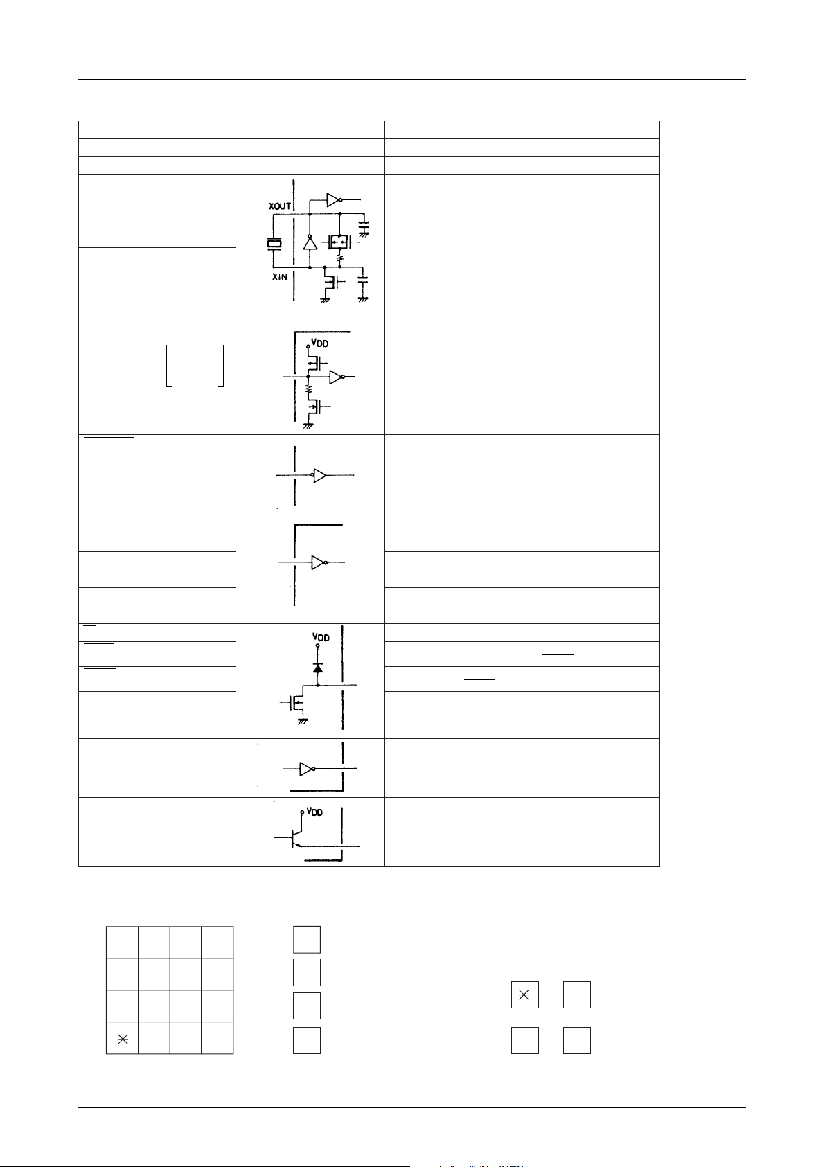
Pin Description ( ) : Pin number of MFP
emaNniP.oNniPnoitarugifnoCO/InoitcnuF
V
DD
V
SS
NIX9
TUOX01
)51(11.nipylppusrewoP
)61(21
)31(
)41(
LC7367J, 7367JM
.ycneuqerfecnereferehtetarenegotdesU
.zHM545975.3forotanoserlatsyrcasesU
mrofotdeniatnocsroticapacdnarotsiserkcabdeefehthtiW
detcennocylpmissirotanoserlatsyrca,tiucricCSOeht
.snipehtssorca
foroticapaca,rotanosercimarecagnisunehW
.niphcaeotdetcennocebtsumFp03yletamixorppa
4Rot1R
4Cot1C
KOOH-FFO5
RPD6
T/P7
RMB8
PD)32(71.tuptuoesluplaiD
1ETUM61
2ETUM51
TUO-EDOM31
4ot1
91ot22
3ot1
6
52
03ot82
)7(
)8(
)9(
)01(
)22(
)12(
)71(
.tupnievitca-hgiH.niptupninmulocdnawoR
-Nnadnanacsdraobyekrofrotsisnartlennahc-PasniatnoC
.nwod-lluprofrotsisnartlennahc
sirotsisnartlennahc-Peht,etatsKOOH-NOehtninehW
.NOdenrutsirotsisnartlennahc-NehtdnaFFOdenrut
KOOH-NO=level-H.tupniWSKOOH
KOOH-FFO=level-L
.tupnitcelesetaresluplaiD
spp02=level-H
spp01=level-L
.tupnitcelesenot/esluP
edomesluP=level-H
edomFMTD=level-L
.tupnitcelesetarekaM
%2.33=level-H
%04=level-L
.edomESLUP-TUPTUOehttasetarepO.tuptuoetuM
.2ETUMhtiwdeRO-deriwgniebfoelbapaC
gniebfoelbapaC.edomFMTDehttasetarepO.tuptuoetuM
.1ETUMhtiwdeRO-deriw
.tuptuoedomESLUP-TUPTUO/FMTD
level-L=edomESLUP-TUPTUO
ecnadepmi-H=edomFMTD
ENOT-K81
FMTD41
Key Assignment
123F
456P
789RD
0#MC
C1 C2 C3 C4
)42(
)81(
F
R1
R2
: Flash
P
: Pause
.tuptuosilangisFMTDehT
When in OUTPUT-PULSE mode
=
RD
R3
R4
: Redial, pause release
MC # RD
: Pulse=tone select
=
.tuptuosism05/zH3421fo)enotreificap(ENOT
.tuptuorewollofrettimedesu-rotsisnartNPN
P
-Keht,edomESLUP-TUPTUOehttadehsupsiyekanehW
No.3095–3/12
Page 4
LC7367J, 7367JM
Specifications
Absolute Maximum Ratings at Ta = 25˚C
retemaraPlobmySsnoitidnoCsgnitaRtinU
egatlovylppusmumixaMV
egatlovtupnimumixaMV
egatlovtuptuomumixaMV
noitapissidrewopelbawollAxamdP 003Wm
ecnatsiserdaolmuminiMR
erutarepmetgnitarepOrpoT 07+ot03–
erutarepmetegarotSgtsT 521+ot04–
Allowable Operating Conditions at Ta = –30 to +70˚C, VDD=1.5 to 6.0V
retemaraPlobmySsnoitidnoC
egatlovylppuS
egatlovlevel-HtupnIV
egatlovlevel-LtupnIV
ecnatsisertcatnocyeKR
ecnaticapacdraobyeKC
noitacificepsrotanoseR
DD
NI
TUO
Ta=70˚C
nimVdnaFMTDssorcA
L
V
PDD
V
TDD
HI
LI
IK
IK
f %7.0±zHM545975.3
SR 001< Ω
edomFMTD0.20.6V
sniptupnillA
sniptupnillAV
nip001
SS
edomESLUP-TUPTUO5.10.6V
Vot3.0–
Vot3.0–
sgnitaR
nimpytxam
V7.0
DD
SS
7+ot3.0–V
3.0+V
DD
3.0+V
DD
Ω
˚C
˚C
tinU
V
V
DD
V3.0
V
DD
0.3kΩ
033Fp
Electrical Characteristics at Ta = 25˚C, VDD=1.5 to 6.0V
retemaraPlobmySsnoitidnoC
I
tnerrucgnitarepO
tnerruCtnecseiuQI
egatlovnoitneterataDV
tnerrucnoitneterataDI
tnerruclevel-HtupnII
tnerruclevel-LtupnII
tnerrucnipyeK
tnerrucegakaeletats-FFOtuptuOI
egatlovniplevel-HtuptuOV
egatlovniplevel-LtuptuOV
AC Characteristics at Ta = 25˚C, VDD=1.5 to 6.0V, f
retemaraPlobmySsnoitidnoC
emitecnuobedyeKT
ycneuqerfENOT-Kf
emittuptuoENOT-KT
emitesuapotuAT
tuptuoenotelgniSV
oitartuptuoenoTd
noitrotsidtuptuoenoT%
emittratsnoitallicsOT
emittuptuoFMTDT
esuaptigidretniFMTDT
emithsalFT
PDD
I
TDD
)TS(DD
nepo
RD
VDDV1= 5.0Aµ
RD
HI
LI
I
I
V
KHI
V
V
KHO
V
FFO
HO
V
LO
V
V,V5.1=
DD
V,V0.6=
DD
V,V5.1=
DD
V,V0.6=
DD
V=0V
DDV,DD
V:ENOT-K
V:ENOT-K
I,V5.1=
DD
I,V5.3=
DD
OSC
DK
TK
TK
PA
RO
V
RCB
DD
V
DD
SID
V
DD
V
DD
TRATS
V
V5.3= 8sm
DD
NOFM
FFOFM
HSALF
sgnitaR
nimpytxam
V,nepotuptuo,edomESLUP-TUPTUO
V5.3=3.05.0Am
DD
V5.3=5.00.1Am
tuptuo,V0.6ot5.1=
V,nip)RMB,T/P,RPD,KOOH-FFO(
HIV=DD
V,nip)RMB,T/P,RPD,KOOH-FFO(
LIV=SS
,1ETUM,PD(,FFOtuptuo,V6=
Aµ521–=
Aµ005–=V
:)nipTUO-EDOM,2ETUM,1ETUM,PD,ENOT-K(
:)nipTUO-EDOM,2ETUM,1ETUM,PD,ENOT-K(
1–Aµ
VDD5.0–
1–V
DD
1Aµ
1V
1Aµ
02Aµ
003Aµ
05–Aµ
007–Aµ
1Aµ
4.0V
4.0V
HIV=DD
HIV=DD
HO
HO
DD
DD
LO
LO
V=nipKOOH-FFO
DDV,DD
V8.0=
V8.0=
)TUO-EDOM,2ETUM
I,V5.1=
I,V5.3=
Aµ521=
Aµ005=
V,nepotuptuo,edomFMTD
DD
DD
DD
HO
HO
=3.579545MHz
sgnitaR
nimpytxam
8.016.11sm
3421zH
9.05sm
99.3s
V,tuptuoENOTWOR
R,V6ot2=
k01= Ω 123Bd
L
R,V6ot5.2=
L
R,V6ot2=
k01= Ω zH0043ot003=f,01%
L
V6ot7.1= 02sm
R,V5.3=
DD
k01= Ω zH0043ot003=f,7%
k01= Ω 071502542smrVm
L
6.79sm
6.001sm
506sm
tinU
V
tinU
No.3095–4/12
Page 5

• Dial Pulse Output
RPDniPRMBniPetaResluPlaiDesuaPtigidretnIoitaRekaM
V
SS
V
DD
V
SS
V
DD
V
DD
V
DD
V
SS
V
SS
SPP49.9sm1.838%2.33
SPP98.91sm6.915%2.33
SPP49.9sm8.448%04
SPP98.91sm0.325%04
• DTMF Output
tupnI
1R7961.99603.0+
2R0772.66794.0–
3R2584.74845.0–
4R1490.84947.0+
1C90219.512175.0+
2C63317.133123.0–
3C77419.174153.0–
dradnatSMJ7637,J7637CL
)zH(ycneuqerFtuptuO
• Redial Operation
fosc=3.579545MHz
retemaraP
tuptuOFMTDsm6.79sm6.001
esuaPtigidretnIsm6.001sm6.001
doirePsm2.891sm2.102
emiT
tigiDts1drawnotigiDdn2
LC7367J, 7367JM
fosc=3.579545MHz
fosc=3.579545MHz
)%(noitaiveD
Timing Charts
(1) OUTPUT-PULSE mode
No.3095–5/12
Page 6

(2) T one mode
(3) Pulse → tone mix (P/T=’H’)
LC7367J, 7367JM
(4) Pulse → tone (P/T=’H’)
No.3095–6/12
Page 7

LC7367J, 7367JM
(5) Timing of flash
(6) Mix dial and redial (key entry available after redial) by P/T input (slide SW, stc.)
• Even when the tone mode (P/T SW : “Tone”) is entered at the OFF-HOOK state, the OUTPUT-PULSE mode can be
entered (P/T SW : “Pulse”).
• The output mode provided when redialing is the one provided when dialed previously (regardless of the P/T SW
position when the RD key is pushed).
• The mode after completion of redialing is set again by the P/T SW position provided when redialing is completed.
Since the DP, MUTE1, MUTE2, MODE-OUT outputs are of the Nch open drain type, the output transistor OFF-state
(H-impedance) provides H-level.
Likewise, since the DTMF output is of the emitter follower type, the output transistor OFF-state (H-impedance)
provides L-level.
No.3095–7/12
Page 8

LC7367J, 7367JM
Key Operation
(1) Normal dial
Off-hook → · · · ·
Redial
Off-hook →
(2) PBX dial
Off-hook → · · · ·
Redial
Off-hook →
(3) Pulse/tone mix
¡ In case where there is no pause during mode select.
Off-hook → (P/T=H)
Redial
Off-hook → D1, D2 D3, D4
™ In case where there are pauses during mode select.
Off-hook → (P/T=H)
Ridial
Off-hook → D1, D2 – D3, D4
D1 D2 Dn
RD
D0 P D1 D2 Dn
RD
D1 D2 MC D3 D4
pulse Tone
RD
D1 D2 MC D3 D4
pulse
RD
RD
Puse
P
4sec
Puse Tone
Tone
T one
(Note) a When in OUTPUT-PULSE mode = =
b Pause : 4s. / 1 push of , 8s. / 2 pushes of , 4×ns. / n pushes of
c For pause release, push . All pauses can be also released by pushing once.
P P
RD
P X RD #
P
RD
Function Specifications
The LC7367J, 7367JM are capable of pulse dial, DTMF dial and also both types of dialing mixed, as well as redial of
these.
1) Dial Output Specifications
• The output pulse make ratio of OUT-PULSE mode can be set at 33.2 or 40% using the BMR pin.
• The output pulse rate of OUT-PULSE mode can be set at 20 or 10pps using the DPR pin.
• 12 types of DTMF dial signals (1 to 0, , #) are generated in DTMF mode.
• DTMF signals are output continuously when the keys are pressed.
• A minimum output for DTMF of approximately 100ms, and also about 100ms for minimum IDP are guaranteed.
2) Summary of Operation
• Key input data is written consecutively in the 31 digit buffer memory (also used as RD memory ; hereinafter
referred to as RD memory).
• The dial data in the RD memory is read out according to the set dial rate, and is output at the DP and DTMF pins.
• Dial output of more than 31 digits is enabled by rewriting the key data from the top (address 0) of the RD memory.
• Because of this, the correct dial does not remain in the RD memory for 32 digits or more, so redial for 32 digits or
more is prohibited.
• Dial data (1 to 0, , #), mode change data (MC) and pause data (P) are written in the RD memory as 1 digit each.
• Dial output mode switching can be performed using the MC key on the key matrix or the P/T input pin.
• The dial output can be stopped for 4 seconds with the pause key (P).
• One-touch redial can be done using the redial key (RD).
Continued on next page.
No.3095–8/12
Page 9

LC7367J, 7367JM
Continued from preceding page.
3) Key and P/T Pin Descriptions
¡ Keys 1 to 0
These are dial data keys. Data is written in the RD memory.
™ , # Keys
In DTMF mode : and # dial data key
In OUT-PULSE mode : = pause key (P)
# = redial key (RD)
The and # keys for DTMF mode and key in the OUT-PULSE mode are for writing data in the RD memory.
£ F Key (flash key)
· The same operation as for 0.6-second hooking is performed when DP output is turned on for 0.6 second.
· Redial can be performed after flash operation.
¢ RD Key (redial key)
1. Redial operation
When the RD key is pressed after hooking (OFF-HOOK pin) or F key operation, the number that immediately
precedes will be redialed.
Redial is prohibited if the number has 32 digits or more.
2. Pause release
The Pause key provides 4-second pause and releases pause attendant on the mode change (MC key, P/T pin).
Even if there is a succession of 2 digits or more of pause data in the RD memory, it will all be released.
∞ P Key (pause key)
· Stops dial output for 4 seconds.
· Data is written in the RD memory.
§ MC Key (mode change key)
· Switches dial mode from OUT-PULSE mode to DTMF mode.
· The mode cannot be switched from DTMF mode to OUT-PULSE mode.
¶ P/T Pin
· Input to indicate dial mode
H=OUT-PULSE mode
L=DTMF (tone) mode
· The mode can be switched between DTMF and pulse mode differ from in case of MC key.
· Mix dialing by P/T pin switching during dialing is possible. MD data is written in the RD memory at this time.
· At OUT-PULSE mode, if the MC key is pressed during dialing, data is written in the RD memory as MC data.
· At OUT-PULSE mode, pressing the first digit (after OFF-HOOK) MC key switches the dial mode, but data is
not written in the RD memory.
Key Assignment
C1 C2 C3 C4
123F
R1
456P
R2
789RD
R3
R4
0#MC
Key Debounce Time
• A key debounce circuit is built in key input to prevent misoperation caused by switch chattering.
Input is valid when on continuously for 11ms or more,
and is invalid when off continuously for 11ms or more.
No.3095–9/12
Page 10

LC7367J, 7367JM
4) MC Data Writing in RD Memory
• After the MC data is stored once in the MC data flag, it is written in the RD memory when another data key
(1 to 0, , #, P) is pressed.
• The MC data flag is reset with hooking and the P key.
• The contents of the MC data flag are canceled and are not written in the RD memory when the P/T pin is switched
as P → T → P.
5) Notes on Dial Specifications
¡ Pause operation during mode switching
When there is no P data before or after MC data.
1. Normal dial
Mode change is done and DTMF data key is started during dial pulse output :
→ After dial pulse ends, pause begins, and the DTMF signal is output with release using the RD key.
DTMF data keyed in after dial pulse output :
→ DTMF signal is output with key-in.
2. Redial for the above
After dial pulse ends, pause begins, and the DTMF signal is output with release using the RD key.
™ Key input during redial
This is ignored except for the F key and the RD key during pause operation.
6) Test Mode
A high speed test mode is provided in order to reduce the IC test time.
• Test mode setting and release methods
BMR pin input
OFF-HOOK pin input
+ built-in power-on reset pulse
• Test mode summary
The internal divider circuit (72 divisions) is bypassed.
Key scan frequency ......72 times
Dial pulse rate ..............72 times
4-second pause ............. 1/72
No.3095–10/12
Page 11

Sample Application Circuit
(Pin numbers are for DIP package)
LC7367J, 7367JM
No.3095–11/12
Page 12

LC7367J, 7367JM
Specifications of any and all SANYO products described or contained herein stipulate the performance,
characteristics, and functions of the described products in the independent state, and are not guarantees
of the performance, characteristics, and functions of the described products as mounted in the customer's
products or equipment. To verify symptoms and states that cannot be evaluated in an independent device,
the customer should always evaluate and test devices mounted in the customer's products or equipment.
SANYO Electric Co., Ltd. strives to supply high-quality high-reliability products. However, any and all
semiconductor products fail with some probability. It is possible that these probabilistic failures could
give rise to accidents or events that could endanger human lives, that could give rise to smoke or fire,
or that could cause damage to other property. When designing equipment, adopt safety measures so
that these kinds of accidents or events cannot occur. Such measures include but are not limited to protective
circuits and error prevention circuits for safe design, redundant design, and structural design.
In the event that any or all SANYO products(including technical data,services) described or
contained herein are controlled under any of applicable local export control laws and regulations,
such products must not be exported without obtaining the export license from the authorities
concerned in accordance with the above law.
No part of this publication may be reproduced or transmitted in any form or by any means, electronic or
mechanical, including photocopying and recording, or any information storage or retrieval system,
or otherwise, without the prior written permission of SANYO Electric Co. , Ltd.
Any and all information described or contained herein are subject to change without notice due to
product/technology improvement, etc. When designing equipment, refer to the "Delivery Specification"
for the SANYO product that you intend to use.
Information (including circuit diagrams and circuit parameters) herein is for example only ; it is not
guaranteed for volume production. SANYO believes information herein is accurate and reliable, but
no guarantees are made or implied regarding its use or any infringements of intellectual property rights
or other rights of third parties.
This catalog provides information as of May, 2001. Specifications and information herein are subject to
change without notice.
PS No.3095–12/12
 Loading...