

Page 1
Ordering number : ENN*6853
11901RM (OT) No. 6853-1/34
Overview
The LC73101C is a dot matrix LCD driver IC that
includes an on-chip display data RAM with a one-to-one
correspondence between bits in RAM and display pixels
on the LCD panel. The LC73101C provides display data
RAM that can store 80 × 132 bits of data and can
implement a large-screen display system with a single
chip.
The LC73101C provides 80 common output circuits and
132 segment output circuits, and can display up to 80 ×
132 dots (8 characters × 4 lines of kanji text using a 16 ×
16-dot kanji font) with a single chip. The LC73101C also
provides a master/slave function that allows two
LC73101C chips to be combined to implement twice the
display area: 160 × 132 dots.
The LC73101C provides a partial display function that
allows the number of lines displayed to be set to 8, 16, 24,
32, 40, 48, 56, 64, 72, or 80 lines by commands sent from
the system microcontroller. This allows the current drain
to be reduced significantly when only a smaller number of
lines needs to be displayed.
This device includes built-in voltage step-up circuits with
factors of 3×, 4×, 5×, and 6× to provide high-quality
display even when a high duty cycle is required. The
number of step-up circuit stages used can be set by
commands from the system microcontroller.
Since the display RAM read and write operations do not
require the external operating clock, the LC73101C can
operate at low power. Furthermore, since the LC73101C
provides built-in LCD drive power supply, LCD drive
power supply voltage adjustment, temperaturecompensated reference voltage, and display contrast
adjustment electronic potentiometers circuits, the
LC73101C can implement portable display systems with
low power consumption and a minimal number of external
components.
Features
• 132 × 80-dot display
• Microcontroller interface (for both Intel and Motorola
microcontrollers)
• On-chip display RAM (80 × 132 = 10,560 bits)
• Low power
• Low-voltage operation: VDD= 1.8 to 3.6 V
• High-precision reference voltage circuit (Variable
temperature compensation coefficients)
• LCD drive 6× voltage step-up circuit (3×, 4×, 5×, or 6×
can be selected by commands from the microcontroller.)
• Built-in high-precision RC oscillator circuit
• Contrast adjustment electronic potentiometer circuit
• Partial display function (Allows 8, 16, 24, 32, 40, 48,
56, 64, 72, or 80 lines to be displayed under the control
of commands sent from the microcontroller.)
• Supports synchronous operation using master/slave
connection.
Preliminary
LC73101C
SANYO Electric Co.,Ltd. Semiconductor Company
TOKYO OFFICE Tokyo Bldg., 1-10, 1 Chome, Ueno, Taito-ku, TOKYO, 110-8534 JAPAN
LCD Driver IC
CMOS IC
Any and all SANYO products described or contained herein do not have specifications that can handle
applications that require extremely high levels of reliability, such as life-support systems, aircraft’s
control systems, or other applications whose failure can be reasonably expected to result in serious
physical and/or material damage. Consult with your SANYO representative nearest you before using
any SANYO products described or contained herein in such applications.
SANYO assumes no responsibility for equipment failures that result from using products at values that
exceed, even momentarily, rated values (such as maximum ratings, operating condition ranges, or other
parameters) listed in products specifications of any and all SANYO products described or contained
herein.
Page 2

Block Diagram
No. 6853-2/34
LC73101C
RES
P/S
WR(R/W)
RD(E)
A0
CS2
CS1
D7(SI)
D6(SCL)
D5
D4
D3
D2
D1
D0
MPU interface
Command decoder Status register
Display data RAM
132 x 80
Column address circuit
Display data latch circuit
Line address circuit
I/O buffer
Page address circuit
Power
supply
circuit
SEG Drivers
SEG0
SEG131
COM Drivers
V
SS
V
DD
V
1
V
2
V
3
V
4
V
5
COM output
status select
circuit
Display timing generation circuit
CAP1+
CAP1-
CAP2+
CAP2-
CAP3+
CAP3-
CAP4+
VOUT
V
SS2
V
R
V
RS
IRS
Bus holder
Oscillator
circuit
CLS
FRS
FR
CL
M/S
HPM
DOF
COM0
COM79
CAP4-
CAP5+
CAP5-
V
EV
Page 3
No. 6853-3/34
LC73101C
Pin Functions
Power supply
Pin I/O Function Number of pins
V
DD
Power supply Microcontroller power supply. The same power supply system must be used for VCC. Undetermined
V
SS
Power supply Connect to the system ground. These pins are 0 V pins. Undetermined
V
SS2
Power supply LCD drive step-up voltage circuit reference voltage Undetermined
V
RS
Power supply
LCD power supply voltage adjustment circuit external input V
REG
power supply.
Undetermined
When the internally generated V
REG
is used, this pin outputs that V
REG
voltage.
Multi-level power supply system used as the LCD power supply. The voltages stipulated for each LCD cell are
created by resistor divider circuits or by operational amplifier based impedance conversion. The potentials are
V
1
, V2, determined referenced to VSS, and must obey the following inequalities.
V
3
, V4, Power supply V1≥ V2≥ V3≥ V4≥ V5≥ V
SS
Undetermined
V
5
When the built-in power supply circuit that operates in master mode is turned on, the voltage determined by the
voltage adjustment circuit is applied to V
1
, and the voltages determined by LCD Bias Set commands are
applied to V
2
through V5.
LCD Power Supply Circuit Pins
Pin I/O Function Number of pins
CAP1+ O
Step-up circuit capacitor positive connection
Undetermined
Insert a capacitor between this pin and the CAP1– pin.
CAP1– O
Step-up circuit capacitor negative connection
Undetermined
Insert a capacitor between this pin and the CAP1+ pin.
CAP2+ O
Step-up circuit capacitor positive connection
Undetermined
Insert a capacitor between this pin and the CAP2– pin.
CAP2– O
Step-up circuit capacitor negative connection
Undetermined
Insert a capacitor between this pin and the CAP2+ pin.
CAP3+ O
Step-up circuit capacitor positive connection
Undetermined
Insert a capacitor between this pin and the CAP3– pin.
CAP3– O
Step-up circuit capacitor negative connection
Undetermined
Insert a capacitor between this pin and the CAP3+ pin.
CAP4+ O
Step-up circuit capacitor positive connection
Undetermined
Insert a capacitor between this pin and the CAP4– pin.
CAP4– O
Step-up circuit capacitor negative connection
Undetermined
Insert a capacitor between this pin and the CAP4+ pin.
CAP5+ O
Step-up circuit capacitor positive connection
Undetermined
Insert a capacitor between this pin and the CAP5– pin.
CAP5– O
Step-up circuit capacitor negative connection
Undetermined
Insert a capacitor between this pin and the CAP5+ pin.
V
OUT
O Post-step-up circuit voltage output. Insert a capacitor between this pin and VSS. Undetermined
Voltage adjustment. Apply a voltage in the range V
1
to VSSby using a resistor divider circuit.
V
R
I Use of this pin is only valid when the built-in V1voltage adjustment resistor is not used (IRS = low). Undetermined
Do not use this pin if the built-in V
1
voltage adjustment resistor is used (IRS = high).
Page 4

No. 6853-4/34
LC73101C
System Bus Connection Pins
Pin I/O Function Number of pins
Bidirectional 8-bit data bus connected to the microcontroller data bus.
When the serial interface is selected (P/S is low):
D0 to D7 I/O
D7: Serial data input (SI)
8
D6: Serial clock input (SCL)
In this mode, D0 to D5 go to the high-impedance state. When the chip select line is inactive, D0 to D7 go to the
high-impedance state.
A0 is normally connected to the low order bit of the microcontroller address bus and discriminates between data
A0 I
and commands.
1
A0 = high: Indicates that D0 to D7 are used for data display.
A0 = low: Indicates that D0 to D7 are used for control data.
RES I
The LC73101C is initialized when RES is set low.
1
The reset operation is performed by the RES signal level.
CS1
I
Chip select signals. The LC73101C becomes active when CS1 is low and CS2 is high. Input and output of data
2
CS2 and commands is possible in this state.
This pin is active-low when an Intel-type microcontroller is used.
RD I
The Intel-type microcontroller RD signal should be connected to this pin. The LC73101C data bus goes to the
1
(E)
output state when this signal is low.
This pin is active-high when a Motorola-type microcontroller is used.
This pin functions as the enable clock input pin when a Motorola-type microcontroller is used.
This pin is active-low when an Intel-type microcontroller is used.
The Intel-type microcontroller WR signal should be connected to this pin. The data bus signals are latched on the
WR
I
rising edge of the WR signal.
(R/W) When a Motorola-type microcontroller is used:
This pin functions as the read/write control signal input.
R/W = high: Read, R/W = low: Write.
C86 is the Microcontroller interface switching input.
C86 I C86 = high: Motorola-type interface 1
C86 = low: Intel-type interface
Parallel/serial data input mode switch
P/S = high: Parallel input
P/S = low: Serial input
The table below lists the effects of this pin.
P/S I 1
When P/S is low, D0 to D5 go to the high-impedance state.
D0 to D5 may be left high, low, or open in this mode.
RD (E) and WR (R/W) must be held either high or low.
In serial data input mode, the RAM display data and the device status cannot be read.
Selects enabled/disabled for the internal oscillator circuit for display clock 1
CLS I
CLS = high: Internal oscillator circuit enabled.
CLS = low: Internal oscillator circuit disabled. (External input)
If CLS is low, input the display clock signal to the CL pin.
Selects master or slave mode operation for the LC73101C itself.
In slave mode operation, synchronization with the display system is acquired by input of the timing signals
required for LCD display.
M/S = high: Master operation
M/S = low: Slave operation
M/S I The M/S and CLS pins determine the operating state as shown in the table below.
1
P/S Data/command Data Read/write Serial clock
“H” A0 D0 to D7 RD, WR —
“L” A0 SI (D7) Write only SCL (D6)
M/S CLS Oscillator circuit Power supply circuit CL FR DOF
“H”
“H” Enabled Enabled Output Output Output
“L” Disabled Enabled Input Output Output
“L”
“H” Disabled Disabled Input Input Input
“L” Disabled Disabled Input Input Input
Page 5
Pin I/O Function Number of pins
LCD segment drive outputs.
One of the V
1
, V3, V4, and VSSlevels is selected by the combination of the contents of display RAM and the
FR signal.
SEG0 to
O 132
SEG131
LCD common drive outputs.
One of the V
1
, V2, V5, and VSSlevels is selected by the combination of the scan data and the FR signal.
COM0 to
O 80
COM80
No. 6853-5/34
LC73101C
Pin I/O Function Number of pins
Display clock input or output.
The M/S and CLS pins determine the operating state as shown in the table below.
CL I/O 1
When two LC73101C chips are used together in master/slave mode, their CL pins must be connected together.
LCD alternation signal input or output.
FR I/O
M/S = high: Output
1
M/S = Low: Input
When two LC73101C chips are used together in master/slave mode, their FR pins must be connected together.
Indicates the on/off state of the LCD display.
M/S = high: Output
DOF I/O M/S = Low: Input 1
When two LC73101C chips are used together in master/slave mode, their DOF pins must be connected
together.
V1 voltage adjustment resistor selection.
IRS = high: Internal resistor used.
IRS I IRS = low: Internal resistor not used. In this case, the V
1
voltage is adjusted by the VR pin and the external 1
divider resistor circuit.
This pin is only valid in master mode. This pin must be held either low or high for slave mode operation.
LCD drive power supply circuit power control.
HPM I
HPM = high: Normal mode
1
HPM = low: High power mode
This pin is only valid in master mode. This pin must be held either low or high for slave mode operation.
Continued from preceding page.
M/S CLS CL
“H”
“H” Output
“L” Input
“L”
“H” Input
“L” Input
RAM data FR
Output voltage
Display positive level Display inverted level
HHV
1
V
3
HLV
SS
V
4
LHV
3
V
1
LLV
4
V
SS
Power saving mode — V
SS
Scan data FR Output voltage
HHV
SS
HLV
1
LHV
2
LLV
5
Power saving mode — V
SS
LCD Drive Pins
Pin I/O Function Number of pins
TEST0
O IC test pins. These pins must be left open. 8
to 7
TEST8 I IC test pin. This pin must be left open. 1
Test Pins
Page 6

Functional Description
Microcontroller Interface
• Interface type selection
The LC73101C transfers data over either an 8-bit bidirectional data bus (D0 to D7) or a serial data input system (SI).
Applications can select either 8-bit parallel data input or serial data input as shown in table 1 by setting the P/S pin
either high or low.
• Parallel interface
When the parallel interface is selected (P/S = high), the bus of either an Intel-type or a Motorola-type microcontroller
can be directly connected to the LC73101C parallel interface by setting the C86 pin either high or low as shown in
table 2.
• Serial interface
When the serial interface is selected (P/S = low), data can be written to the LC73101C using the serial input (SI) and
serial clock (SCL) pins with the chip in the active state (CS1 = low, CS2 = high). The serial interface consists of an 8bit shift register and a 3-bit counter. Serial data is acquired from the serial data input pin in the order D7 to D0 on the
rising edge of the serial clock signal. The serial data is converted to 8 bits of parallel data on the eighth rising edge of
the serial clock and processed by the LC73101C.
Whether the serial data input is display data or a command is determined by the state of the A0 input. When A0 is high,
the data is display data, and when A0 is low, it is taken to be a command. The A0 input is acquired and interpreted
once every eight rising edges (that is, on the 8×th rising edge) of the serial clock signal after the chip goes to the active
state.
Figure 1 shows the timing chart for the serial interface.
When the chip is in a non-active state due to the CS1 and CS2 inputs, the shift register and the counter are reset. The
serial interface does not support readout. Be sure to prevent termination reflections and noise from appearing on the
SCL signal. We recommend testing in an actual end product.
No. 6853-6/34
LC73101C
Table 1
P/S CS1 CS2 A0 RD WR C86 D7 D6 D5 to D0
High: Parallel input CS1 CS2 A0 RD WR C86 D7 D6 D5 to D0
Low: Serial input CS1 CS2 A0 — — — SI SCL High impedance
Table 2
C86 CS1 CS2 A0 RD WR D7 to D0
High: Mptorola-type MPU bus CS1 CS2 A0 E R/W D7 to D0
Low: Intel-type MPU bus CS1 CS2 A0 RD WR D7 to D0
Figure 1
P/S
CS1
CS2
SCL(D6)
SI(D7)
ParallelData
(InternalDataBus)
A0
XXH
X
D7 D6 D5 D4 D3 D2 D1 D0 D7 D6 D5 D4 D3 D2
XX
Data or
Command
D7:000H
00H
Page 7
• Chip select
The LC73101C has two chip select inputs: CS1 and CS2. The microcontroller and the serial interface can only be used
when CS1 is low and CS2 is high. When the chip select inputs select a non-active state, the D0 to D7 pins go to the
high-impedance state and the A0, RD, and WR inputs are disabled. The serial interface shift register and counter are
reset.
• Access to display data RAM and internal registers
The LC73101C supports high-speed data transfers that require no wait time as long as the LC73101C access cycle time
constraints are met by the microcontroller. The LC73101C uses an internal “bus holder” circuit on its internal data bus
to receive or send data during data transfers with the microcontroller.
For example, when the microcontroller writes to LC73101C display data RAM, the data is temporarily held by the bus
holder and written to the display data RAM before the next write cycle. When the microcontroller reads out the
contents of the display data RAM, data read out on the first (dummy) read cycle is stored in the bus holder, and then
that data is read out onto the system bus on the next data read cycle. When reading display data RAM, after setting the
address, the immediately following read instruction does not read out the data at the address specified, but rather reads
out the data from the address specified by the second preceding data read operation. Thus care is required when using
this function. This means that one dummy read operation is always required after setting the address or after a write
cycle. Figure 2 (a) and figure 2 (b) show this timing.
• Busy flag
When the busy flag is high, it indicates that an LC73101C internal operation is in progress.
The busy flag is output from the D7 pin by a Status Read command. If the cycle time (t
CYC
) conditions are met, there
is no need to check this flag before each command. This can significantly increase the available processing power of
the microcontroller.
No. 6853-7/34
LC73101C
(a) Read
N
WR
RD
DATA
N
Address N N+1 N+2
Address Preset
Read Signal
Column Address
Bus Holder
MPUInternal timing
Unknown Data N Data N+1
Address Set
Dummy
Read
Data Read
N+1
Data Read
N
WR
DATA
N+1 N+2 N+3
N N+1 N+2 N+3
BUS Holder
RAM Write Signal
MPU
Internal
timing
(a) Write
Latch
Data Write Complete
Page 8
Display Data RAM
• Display data RAM
The display data RAM holds the dot data to be displayed, and has an 80 (10-page × 8-bit) × 132-bit organization. This
memory is accessed by specifying a page address and a column address to access data in 8-bit units. Since the display
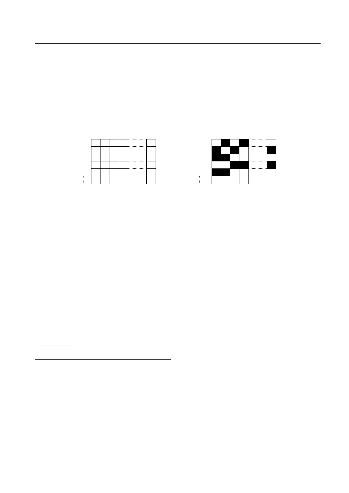
data D7 to D0 from the microcontroller corresponds to the direction of the LCD common pins as shown in figure 3,
when two LC73101C chips are used together, there are few constraints or limitations when transferring data, and
highly flexible display structures can be implemented easily. Read and write operations to this display data RAM are
performed through an I/O buffer, and thus these operations are independent of signal reads for LCD drive. This means
that flicker and other problems do not occur when the display RAM is accessed asynchronously during display on the
LCD panel.
Figure 3 Noninverting LCD Display
• Page address circuit
The display data RAM page address shown in figure 4 is specified using the Page Address Set command. The page
address must be specified again to access a different page.
• Column address circuit
The display data RAM column address shown in figure 4 is specified using the Column Address Set command. Since
the specified column address is incremented each time a display data read or write command is input, the
microcontroller can access the display data consecutively. Note that this column address incrementing stops when the
column address reaches 83H. Since the column address and the page address are mutually independent, the column
address and the page address must both be specified again to access a different column on a different page.
Additionally, the correspondence between the display data RAM column address and segment output can be inverted
with the CSS command (Column Address/Segment Output Correspondence Selection command) as shown in table 3.
This reduces constraints on IC positioning when assembling LCD modules.
No. 6853-8/34
LC73101C
D0 0 1 0 1 0 COM0
D1 1 0 1 0 1 COM1
D2 1 1 0 0 0 COM2
D3 0 0 1 1 1 COM3
D4 1 1 0 0 0 COM4
Display data RAM LCD display
Table 3
CSS setting (D0) Column address Segment output
0
0H → SEG0
83H → SEG131
1
0H → SEG131
83H → SEG0
Page 9

• Line address circuit
The line address circuit specifies the line address corresponding to the COM output when the contents of display data
RAM are displayed as shown in figure 4. Normally, the Display Start Line Address Set command specifies the
uppermost line of the display (which depends on the common output state: in normal mode: COM0 output; in the
inverted state: COM79 output). The maximum display area is 80 lines in the direction of increasing line address values
from the specified display start line address.
The data for the line address set by the Display Start Line Address Set command is passed to the common output driver
specified by the Common Output State Selection command and the address set by the Display Start Common Address
Set command in the common address circuit.
Operations such as scrolling the screen and switching pages can be implemented by changing display start line address
with this Display Start Line Address Set command.
• Common address circuit
The line address circuit passes the display data for the line address determined by the line address circuit to the
common output driver offset by the number of lines set by the Display Start Common Address Set command.
Additionally, at this time the correspondence (figure 4) between the common output driver and the common address
specified by the Common Output State Selection command is take into consideration.
During partial display, the display position on the screen can be changed by changing this address without rewriting the
contents of display RAM.
• Display data latch circuit
The display data latch circuit is a latch that temporarily holds the display data output to the LCD drive circuit from data
display RAM. Since the display normal/inverted and display on/off commands control this latched data, the data in
display data RAM is not changed by these functions.
No. 6853-9/34
LC73101C
Page 10

Figure 4 Display RAM Address Map
No. 6853-10/34
LC73101C
00H
01H
02H
03H
04H
05H
06H
07H
7CH
7DH
7EH
7FH
80H
81H
82H
83H
01H
02H
03H
04H
05H
06H
07H
08H
09H
0AH
0BH
0CH
0DH
0EH
0FH
00H
11H
12H
13H
14H
15H
16H
17H
18H
19H
1AH
1BH
1CH
1DH
1EH
1FH
10H
21H
22H
23H
24H
25H
26H
27H
28H
29H
2AH
2BH
2CH
2DH
2EH
2FH
31H
32H
33H
34H
35H
36H
37H
38H
39H
3AH
3BH
3CH
3DH
3EH
3FH
41H
42H
43H
44H
45H
46H
47H
48H
49H
4AH
4BH
4CH
4DH
4EH
4FH
20H
30H
40H
Page0
Page2
Page1
Page3
Page4
Page5
Page6
Page7
Page8
Page9
D0
Data
D1
D2
D3
D4
D5
D6
D7
D0
D1
D2
D3
D4
D5
D6
D7
D0
D1
D2
D3
D4
D5
D6
D7
D0
D1
D2
D3
D4
D5
D6
D7
D0
D1
D2
D3
D4
D5
D6
D7
D0
D1
D2
D3
D4
D5
D6
D7
D0
D1
D2
D3
D4
D5
D6
D7
D0
D1
D2
D3
D4
D5
D6
D7
D0
D1
D2
D3
D4
D5
D6
D7
D0
D1
D2
D3
D4
D5
D6
D7
0000
1000
0100
1100
0010
0110
1010
1110
0001
1001
D0D1D2D3
Page
Address
Line
Address
Column
Address
Common
Address
COM0
Start
COM1
COM2
COM3
COM4
COM5
COM6
COM7
COM8
COM9
COM10
COM11
COM12
COM13
COM14
COM15
COM16
COM17
COM18
COM19
COM20
COM21
COM22
COM23
COM24
COM25
COM26
COM27
COM28
COM29
COM30
COM31
COM32
COM33
COM34
COM35
COM36
COM37
COM38
COM39
COM40
COM41
COM42
COM43
COM44
COM45
COM46
COM47
COM48
COM49
COM50
COM51
COM52
COM53
COM54
COM55
COM56
COM57
COM58
COM59
COM60
COM61
COM62
COM63
COM64
COM65
COM66
COM67
COM68
COM69
COM70
COM71
COM72
COM73
COM74
COM75
COM76
COM77
COM78
COM79
00H
1
01H
02H
03H
04H
05H
06H
07H
7CH
7DH
7EH
7FH
80H
81H
82H
CSS
Command
(D0)
83H
0
COM0
COM1
COM2
COM3
COM4
COM5
COM6
COM7
COM8
COM9
COM10
COM11
COM12
COM13
COM14
COM15
COM16
COM17
COM18
COM19
COM20
COM21
COM22
COM23
COM24
COM25
COM26
COM27
COM28
COM29
COM30
COM31
COM32
COM33
COM34
COM35
COM36
COM37
COM38
COM39
COM40
COM41
COM42
COM43
COM44
COM45
COM46
COM47
COM48
COM49
COM50
COM51
COM52
COM53
COM54
COM55
COM56
COM57
COM58
COM59
COM60
COM61
COM62
COM63
COM64
COM65
COM66
COM67
COM68
COM69
COM70
COM71
COM72
COM73
COM74
COM75
COM76
COM77
COM78
COM79
Common Output
Select(D3)
0 1
Common Output
Page 11

Partial Display Function
• Partial display function
The LC73101C provides commands that control the following settings: the LCD drive duty setting, the LCD drive bias
selection, the number of stages of voltage step-up, the display start line address, and the display start common address.
These settings can be used to only display part of the screen.
The number of lines displayed by the partial display function can be selected to be 8, 16, 24, 32, 40, 48, 56, 64, 72, or
80 lines. This is set by setting the LCD duty. The start of the frame is the display start line, and by setting this line to be
the display start common address, it is possible to select any of the COM0 to COM79 lines.
In general, as the LCD drive duty is reduced, the optimal values of the LCD drive voltage and LCD drive bias also
become smaller. Since this allows the number of step-up stages in the voltage step-up circuit to be reduced, power
consumption can be reduced significantly.
• Duty and frame frequency
Table 4 shows the relationship between the duty setting, the number of lines, the display clock frequency fCL, and the
frame frequency fFR.
Oscillator Circuit
This circuit is an RC circuit that generates the display clock. The oscillator circuit is only enabled when M/S is high and
CLS is high. When CLS is low, the oscillator circuit is stopped and the display clock is input to the CL pin.
No. 6853-11/34
LC73101C
Table 4
Duty
Number of lines
fCL[kHz] fFR[Hz]
displayed
80 80 6.40 80.0
72 72 5.12 71.1
64 64 5.12 80.0
56 56 4.27 76.2
48 48 3.66 76.2
40 40 3.20 80.0
32 32 2.56 80.0
24 24 1.97 82.1
16 16 1.28 80.0
8 8 0.640 80.0
Page 12

Display Timing Generator
This circuit generates the timing signals for the line address circuit and the display data latch circuit from the display
clock. The display data is latched by the display data latch circuit in synchronization with the display clock and output to
the segment drive output pins. Readout of the display data to the LCD drive circuit is completely independent of
microcontroller access to the display data RAM. This means that flicker or other problems never occur due to the display
RAM being accessed asynchronously during display on the LCD panel. This circuit also generates the internal common
timing and the LCD alternation signal (FR) from the display clock. The two-frame alternation drive waveforms shown in
figure 5 are generated for the LCD drive circuit.
Figure 5 Frame Alternation Drive Waveforms
When the LC73101C is used in a multi-chip configuration, the display timing signals (FR, CL, and DOF) must be
provided to the slave by the master.
Table 5 shows the states of the FR, CL, and DOF pins.
No. 6853-12/34
LC73101C
CL
7980123456
COM0
FR
COM1
V1
V2
V1
V2
V5
VSS
V5
VSS
V1
V3
V4
VSS
RAM
DATA
SEGn
757677787980123456
Table 5
Setting
FR CL DOF
M/S CLS
“H”
“H” Output Output Output
“L” Output Input Output
“L”
“H” or “L” Input Input Input
“H” or “L” Input Input Input
Page 13

Common Output State Selection Circuit
The LC73101C allows the scan direction of the COM outputs to be set with the common output state selection circuit.
This reduces constraints on IC positioning when assembling LCD modules. (See table 6.)
LCD Drive Circuit
The LCD drive voltages are output according to the combination of the display data, the COM scan signal, and the FR
signal. Figure 6 shows the SEG and COM output waveform examples for the frame alternation drive technique used.
Figure 6
No. 6853-13/34
LC73101C
Table 6
Common Output State Selection command (D3) Selected state
0 Normal: COM0 → COM79
1 Inverted: COM79 → COM0
FR
COM0
COM1
SEG0
SEG1
Vss
Vdd
V1
V2
V3
V4
V5
Vss
V1
V2
V3
V4
V5
Vss
V1
V2
V3
V4
V5
Vss
V1
V2
V3
V4
V5
Vss
SEG0
SEG1
SEG2
SEG3
COM0
COM1
COM2
Page 14

Power Supply Circuit
This circuit is a low power consumption power supply circuit that creates the voltages required for LCD drive. It can only
be used when the LC73101C is in master mode. It consists of a voltage step-up circuit, a voltage adjustment circuit, and a
voltage follower circuit. The on/off states of the voltage step-up circuit and the voltage adjustment circuit in the power
supply can be controlled individually with the Power Control Set command. This allows external power supply levels to
be used in combination with certain of the functions of the internal power supply circuit. Table 7 lists the functions
controlled by the 3 bits of data in the Power Control Set command, and table 8 presents examples of possible
combinations of functions.
• Voltage step-up circuit
The LC73101C's built-in voltage step-up circuit can generate potentials that are 3×, 4×, 5×, and 6× that of the potential
between V
SS2
and VDD. Figure 7 shows the relationships between these potentials.
Figure 7 The relationships between these potentials
No. 6853-14/34
LC73101C
Table 7 Power Control Set Command Bit Functions
Bit Item set
Bit value
10
D2 Voltage step-up circuit ON OFF
D1 Voltage adjustment circuit (V adjustment circuit) ON OFF
D0 Voltage follower circuit (V/F circuit) ON OFF
Table 8 Sample Combinations
D2 D1 D0 Step-up circuit V adjustment circuit V/F circuit
External voltage Step-up system
input pins
1. Only the internal power supply used 1 1 1 ●● ●● ●● V
SS2
Used
2. Only the V adjustment and V/F circuits used 0 1 1 × ●● ●● V
OUT
, V
SS2
Open
3. Only the V/F circuit used 0 0 1 ××●● V
5
, V
SS2
Open
4. External power supply only 0 0 0 ×××V
1
to V
5
Open
Note: The step-up system pins are the CAP1+, CAP1–, CAP2+, CAP2–, CAP3+, CAP3–, CAP4+, CAP4–, CAP5+, and CAP5– pins.
While combinations other than the above are possible, these other combinations are impractical and are not recommended.
VSS2 = 0V
V
DD = 3V
V
OUT = 9V
VSS2 = 0V
V
DD = 3V
V
OUT = 12V
VSS2 = 0V
V
DD = 3V
V
OUT = 15V
VSS2 = 0V
V
DD = 3V
V
OUT = 18V
3 × step-up 4 × step-up 5 × step-up 6 × step-up
Page 15

• Voltage adjustment circuit
The stepped-up voltage generated at the V
OUT
pin is output as the V1LCD drive voltage through the power supply
adjustment circuit. Since the LC73101C provides a reference voltage based on a high-precision constant-voltage
source, an electronic potentiometer with 64 levels, and furthermore, a voltage adjustment resistor built in to the V1pin,
a high-precision voltage adjustment circuit can be implemented with a minimal number of external components. Figure
8 shows this voltage adjustment circuit.
Figure 8 Voltage Adjustment Circuit
The formulas below show the relationship between Ra, Rb, V
REG
, VEV, and V1. The term α is the set value of the
electronic potentiometer.
(1) Reference voltage
The LC73101C includes a constant-voltage supply that features a selectable temperature correction coefficient: one of
three slopes can be selected. The Reference Supply Selection command is used to select the slope. This command can
also be used to isolate (disconnect) the internal low-voltage supply so that the reference voltage can be supplied from the
external VRSpin. The bits D0 and D1 in the Reference Supply Selection command control these settings. Table 9 lists the
reference voltage V
REG
values that correspond to the D0 and D1 settings.
No. 6853-15/34
LC73101C
V
DD
VEV(Reference voltage +
electronic potentiometer)
V1
Internal Ra
(External Ra')
Internal Rb
(External Rb')
(V
R
pin)
+
–
Ra
Rb
V
1
=
V
EV
=
× V
EV
× V
REG
1 +
162
1 –
α
Table 9
D1 D0 Setting V
REG
0 0 Internal reference voltage: Off Input from the VRSpin
0 1 Temperature coefficient: –0.05% –2.5 V
1 0 Temperature coefficient: –0.1% –2.5 V
1 1 Temperature coefficient: –0.2% –2.5 V
Page 16

(2) Electronic potentiometer
The electronic potentiometer function can be used when the voltage adjustment circuit is activated by the Power Control
Set command.
The electronic potentiometer adjusts the reference voltage using a resistor divider. This adjustment is set using the
Electronic Potentiometer Mode Set command and the Electronic Potentiometer Register Set 2-Byte command. Table 10
lists the correspondence between the 6 bits of setting data specified by these commands and the value of the α parameter.
(3) Voltage adjustment using the internal resistor
The internal voltage adjustment resistor can be used when the IRS pin is high. Here, the VR pin should be left open. The
internal resistor ratio (1 + Rb/Ra) can be set with the V1Adjustment Internal Resistor Ratio Set command.
Table 11 lists the correspondence between the 4 bits of data specified by this command and the value of the ratio (1 +
Rb/Ra) set by that command. See the section “V1voltage Adjustment Internal Resistor Ratio Set Command” in the
command descriptions for details on using this command.
(4) Voltage adjustment using external resistors
When the IRS pin is low, the built-in voltage adjustment resistor is disconnected and the voltage can be adjusted using
external resistors. Divide the voltage between VDDand V5with the external resistors Ra' and Rb' and apply that voltage
to the VRpin.
No. 6853-16/34
LC73101C
Table 10
D5 D4 D3 D2 D1 D0 α
00000063
00000162
00001061
↓↓
1111012
1111101
1111110
Table 11
V3V2V1V
0
1 + Rb/Ra
0000 1.5
0001 2.0
0010 2.5
0011 3.0
0100 3.5
0101 4.0
0110 4.5
0111 5.0
1000 5.5
1001 6.0
1010 6.5
Page 17

LCD Voltage Generation Circuit
The V1, V2, V3, and V4potentials required for LCD drive are generated by resistor division of the V1voltage internally
to the IC. The voltage followers are used to convert the impedance of the V1, V2, V3, and V4potentials and supply those
levels to the LCD drive circuit. The bias ratio can be set with the LCD Bias Set command. Table 12 shows the
correspondence between the 6 bits of data specified by this command and value of the bias setting set by that data.
High Power Mode
The power supply circuit built into the LC73101C is an extremely low power consumption circuit in normal mode (when
HPM is high). As a result, the display quality with panels or LCDs that present a relatively large load may be
compromised. In such cases, the display quality can be improved by setting the HPM pin low to switch the LC73101C to
high power mode. We recommend testing in an actual system to decide whether or not to use this mode. Note that it may
be necessary to use an external power supply for LCD drive if high power mode cannot provide adequate display quality.
No. 6853-17/34
LC73101C
Table 12
D2 D1 D0 Bias setting
0 0 0 1/10
0 0 1 1/9
0 1 0 1/8
0 1 1 1/7
1 0 0 1/6
1 0 1 1/5
1 1 0 1/4
Page 18

Reset Circuit
The LC73101C is reset to the initialized state by a low level applied to the RES input. The following describes the
initialized state.
(1) Display: off
(2) Display normal
(3) ADC selection: Normal (ADC command D0 = 0)
(4) Power control register (D2, D1, D0) = (0, 0, 0)
(5) Serial interface internal register data: cleared
(6) LCD power supply bias ratio: 1/10
(7) Display: all dots off.
(8) Power saving function: disabled
(9) V
1
voltage adjustment internal resistors Ra and Rb: Disconnected.
(10) The SEG and COM outputs go to the VSSlevel while RES is low.
(11) Read-modify-write: off
(12) Display start line address: 00H
(13) Display start common address: 00H
(10) Column address: 00H
(11) Page address: page 0
(12) Common output state: Normal order
(13) V1voltage adjustment internal resistor ratio: 1.5
(14) Electronic potentiometer register set mode: cleared
Electronic potentiometer register (D5, D4, D3, D2, D1, D0) = (1, 0, 0, 0, 0, 0)
(15) LCD bias register set mode: cleared
LCD bias register (D2, D1, D0) = (0, 0, 0)
When the Reset command is used, only items (7) to (15) in the above initialization items are reset as shown.
The RES pin can be connected to the microcontroller reset pin so that both the LC73101C and the microcontroller are
reset at the same time. The LC73101C must be initialized with the RES pin when power is first applied. Note that
overcurrents may flow in this IC if the control signals from the microcontroller are in the high-impedance state.
Applications must be designed so that the input pins are not connected to high-impedance lines when power is first
applied. If the internal LCD power supply circuit is not used, the RES pin must be at the low level when the external
LCD power supply is turned on.
No. 6853-18/34
LC73101C
Page 19

Commands
1. Display On/Off
Controls the on/off state of the LCD panel. The D0 bit sets the on/off state of the LCD display.
When a Display Off command is issued in the display fully on (all lit by All Display Pixels Lit On command) state, the
device goes to the power saving state.
2. Display Start Line Set
Sets the line address for the start of display from display data RAM. This address is set in two operations: first the upper
3 bits and then the lower 4 bits. Both the upper and lower bits can be set independently.
At reset, the display start line address is reset to 00H. The display can be scrolled by periodically changing the display
start line address with this command. In partial display mode, the content displayed can be changed without changing the
contents of display RAM by changing the address with this command.
See the functional description in the “Line Address Circuit” section for details.
No. 6853-19/34
LC73101C
A0 RD WR D7 D6 D5 D4 D3 D2 D1 D0 Setting
01010101110 Display off
1 Display on
A0 RD WR D7 D6 D5 D4 D3 D2 D1 D0
0100100XL6L5L4
0 1 0 1 L3L2L1L0
L6 L5 L4 L3 L2 L1 L0 Display start line address
0000000 0
0000001 1
0000010 2
↓↓
1001110 78
1001111 79
Page 20

3. Display Start Common Set
Sets the common address for the start of display from display data RAM. This address is set in two operations: first the
upper 3 bits and then the lower 4 bits. Both the upper and lower bits can be set independently.
At reset, the display start common address is reset to 00H. In partial display mode, the content displayed position can be
changed without changing the contents of display RAM by changing the address with this command.
See the functional description in the “Common Address Circuit” section for details.
4. Page Address Set
Sets the page address used when the display data RAM is accessed from the microcontroller.
The display data RAM is accessed in 8-bit units using a page address and a column address.
At reset, the page address is reset to 0.
See the functional description in the "Page Address Circuit" section for details.
No. 6853-20/34
LC73101C
A0 RD WR D7 D6 D5 D4 D3 D2 D1 D0
0100110XC6C5C4
0 1 1 1 C3C2C1C0
C6 C5 C4 C3 C2 C1 C0 Display Start Common Address
0000000 0
0000001 1
0000010 2
↓↓
1001110 78
1001111 79
A0 RD WR D7 D6 D5 D4 D3 D2 D1 D0 Page address
01010110000 0
0001 1
0010 2
↓↓
1000 8
1001 9
Page 21

5. Column Address Set
Sets the column address for display data RAM. This address is set in two operations: first the upper 4 bits and then the
lower 4 bits. The column address is automatically incremented (+1) each time display data RAM is accessed. Thus there
is no need to issue this command each time this RAM is read or written, and the microcontroller can read or write display
data consecutively.
Automatic increment of the column address stops when it reaches 83H.
See the functional description in the "Column Address Circuit" section for details.
6. Status Read
Allows the microcontroller to read out the IC state from the status data.
7. Display Data Write
Writes 8 bits of data to the address specified for display data RAM. After the write, the column address is automatically
incremented to allow the microcontroller to write display data continuously.
No. 6853-21/34
LC73101C
A0 RD WR D7 D6 D5 D4 D3 D2 D1 D0
0100001M7M6M5M4
0 0 0 0 M3M2M1M0
M6 M5 M4 M3 M2 M1 M0 Column Start Address
0000000 0
0000001 1
0000010 2
↓↓
1000010 130
1000011 131
Busy flag
ST1
When ST1 is 1, indicates that either a read operation or an internal operation is in progress.
This command can be issued until ST1 becomes 0. However, there is no need to check this flag if the cycle time conditions are met.
Indicates the correspondence between column addresses and segment drivers.
ST2 0: Inverted (Column addresses 0H → 83H: SEG0 → SEG131)
1: Normal (Column addresses 0H → 83H: SEG131 → SEG0)
Indicates the on/off state of the display. (This value has the reverse polarity of the Display On/Off command.)
ST3 0: Display on
1: Display off
Indicates that an initialization operation due to either the RES signal or a Reset command.
ST4 0: Operating state
1: Reset in progress
A0 RD WR D7 D6 D5 D4 D3 D2 D1 D0
0 0 1 ST4 ST3 ST2 ST1 1 1 1 1
A0 RD WR D7 D6 D5 D4 D3 D2 D1 D0
1 1 0 Write data
Page 22

8. Display Data Read
Reads 8 bits of data from the address specified for display data RAM. After the read, the column address is automatically
incremented to allow the microcontroller to read display data continuously.
Note that one dummy read is required immediately after the column address is set. It is not possible to read out display
data using the serial interface.
9. Column Address/Segment Output Correspondence Selection
Allows the correspondence between the display RAM data column address and the segment driver outputs to be inverted.
10. Display Normal/Inverted
Allows pixel on/off states to be inverted without rewriting the contents of display data RAM.
The contents of display data RAM are retained unchanged by this operation.
11. All Display Pixels Lit On/Off
Allows all the pixels in the display to be forcibly set to the on state regardless of the contents of display data RAM.
The contents of display data RAM are retained unchanged by this operation.
This command takes priority over the Display Normal/Inverted command.
When a Display All Pixels Lit On command is issued with the device in the display off state, the device goes to the
power saving state.
No. 6853-22/34
LC73101C
A0 RD WR D7 D6 D5 D4 D3 D2 D1 D0
1 0 1 Read data
A0 RD WR D7 D6 D5 D4 D3 D2 D1 D0 Setting
01010100000Normal: Column address 0 → SEG0
Column address 131 → SEG131
1 Inverted:Column address 0 →SEG131
Column address 131 → SEG0
A0 RD WR D7 D6 D5 D4 D3 D2 D1 D0 Setting
01010100110RAM data high → LCD pixel on
1 RAM data low → LCD pixel on
A0 RD WR D7 D6 D5 D4 D3 D2 D1 D0 Setting
01010100100 Normal display state
1 All pixels lit state.
Page 23

12. LCD Bias
These commands select the bias ratio for the voltages required for LCD drive.
These commands form a 2-byte command pair: the Electronic Potentiometer Mode Set command and the Electronic
Potentiometer Register Set command. These two commands must be issued consecutively.
LCD Bias Mode Set
When this command is issued, the LCD Bias Register Set command is enabled. Once the electronic potentiometer mode
is set, no command other than the LCD Bias Register Set command can be used. This state is cleared after data is stored
into the register with the LCD Bias Register Set command.
This command is cleared when a reset input occurs or when a reset command is issued.
LCD Bias Register Set
Stores 3 bits of data into the LCD bias register to select one of 6 bias values.
LCD bias mode is cleared after the LCD bias register is set by issuing this command.
The bias is set to 1/10 if a value other than those listed above is used for D2 to D0.
No. 6853-23/34
LC73101C
A0 RD WR D7 D6 D5 D4 D3 D2 D1 D0
01010100010
A0 RD WR D7 D6 D5 D4 D3 D2 D1 D0 Setting
01000000000 1/10
0 0 1 1/9
0 1 0 1/8
0 1 1 1/7
1 0 0 1/6
1 0 1 1/5
Page 24

13. Read/Modify/Write
Used as a pair with the End command. Once this command has been issued, the column address is not changed by the
Display Data Read command, but is only incremented by the Display Data Write command. This state remains in effect
until an End command is issued. When an End command is issued, the column address returns to the address it held at
the point the Read/Modify/Write command was issued.
14. End
Clears read/modify/write mode and returns the column address to its address at the start of this mode.
Figure 9
15. Reset
Initializes the display start line, column address, page address, common output state, V1voltage adjustment internal
resistor ratio, and electronic potentiometer and clears read/modify/write mode and test mode. A reset has no effect on the
contents of display data RAM. The reset operation is performed after the reset command is issued.
Apply a reset signal to the RES pin for initialization when power is first applied.
The reset state is cleared by issuing a NOP command. A NOP command must be issued after a reset.
No. 6853-24/34
LC73101C
A0 RD WR D7 D6 D5 D4 D3 D2 D1 D0
01011100000
A0 RD WR D7 D6 D5 D4 D3 D2 D1 D0
01011101110
A0 RD WR D7 D6 D5 D4 D3 D2 D1 D0
01011100010
Column address
Read/Modify/Write command End command
N
N+1 N+2
N+
N
Page 25

16. Common Output State Selection
Selects the scan direction for the COM output pins.
The common signals are output sequentially in the scan direction selected with this command from the selected frame
start position for the specified display start common setting.
17. Power Control Set
Specifies the functions of the power supply circuit. See the functional description in the “Power Supply Circuit” section
for details.
18. V1Voltage Adjustment Internal Resistor Ratio Set
Sets the V1voltage adjustment internal resistor ratio. The four bits of this setting are specified using two consecutive
commands: one to set the upper 2 bits, and the other to set the lower 2 bits.
No. 6853-25/34
LC73101C
A0 RD WR D7 D6 D5 D4 D3 D2 D1 D0 Selected state
01011000×××Normal: COM0 → COM79
1 Inverted: COM79 → COM0
A0 RD WR D7 D6 D5 D4 D3 D2 D1 D0 Selected state
010001010 Step-up circuit: Off
1 Step-up circuit: On
0 V adjustment circuit: Off
1 V adjustment circuit: On
0 V/F circuit: Off
1 V/F circuit: On
(V/F circuits: Voltage follower circuit; V adjustment circuit: voltage adjustment circuit)
A0 RD WR D7 D6 D5 D4 D3 D2 D1 D0
010001001V3V2
001000V1V0
V3 V2 V1 V0 1 + Rb/Ra
0000 1.5
0001 2.0
0010 2.5
0011 3.0
0100 3.5
0101 4.0
0110 4.5
0111 5.0
1000 5.5
1001 6.0
1010 6.5
Page 26

19. Electronic Potentiometer
Controls the LCD drive voltage V1output from the internal LCD power supply voltage adjustment circuit and adjusts the
contrast of the LCD display.
These commands form a 2-byte command pair: the Electronic Potentiometer Mode Set command and the Electronic
Potentiometer Register Set command. These two commands must be issued consecutively.
19-1. Electronic Potentiometer Mode Set
When this command is issued, the electronic Potentiometer Register Set command is enabled. Once the electronic
potentiometer mode is set, no command other than the Electronic Potentiometer Register Set command can be used. This
state is cleared after data is stored into the register with the Electronic Potentiometer Register Set command.
19-2. Electronic Potentiometer Register Set
This command sets the LCD drive voltage V1to one of 64 voltage levels by writing 6 bits of data to the electronic
potentiometer register.
Electronic potentiometer mode is cleared after this command is issued and the electronic potentiometer register has been
set.
This register is set to (X, X, 1, 0, 0, 0, 0, 0) when the electronic potentiometer function is not used.
20. Power Save
The LC73101C can be set to its power saving mode by issuing the Display Off command and the All Display Pixels Lit
On command. Power consumption can be reduced significantly by setting the LC73101C to power saving mode.
In power saving mode, the states of the display data and the operating mode prior to power saving mode are retained, and
the microcontroller can access the display data RAM.
Power saving mode is cleared using the All Display Pixels Lit Off command.
In power saving mode, all LCD display system operations are stopped and current can be reduced to a value close to the
quiescent current even when RAM is not accessed by the microcontroller. The internal states in this mode are as follows.
(1) The oscillator circuit and the LCD power supply circuit are stopped.
(2) All LCD drive circuits are stopped and the segment and common driver outputs go to the VSSlevel.
No. 6853-26/34
LC73101C
A0 RD WR D7 D6 D5 D4 D3 D2 D1 D0
01010000001
A0 RD WR D7 D6 D5 D4 D3 D2 D1 D0 α
010××000000 63
000001 62
000010 61
↓↓
111101 2
111110 1
111111 0
Display On/Off All Display Pixels Lit Setting
On Off Power saving mode cleared
On On (normal operating state)
Off Off
Off On Power saving mode
Page 27

21. NOP
This command is the no-op (no operation) command.
Issuing this command has no effects on the IC internal circuits.
22. Reference Supply Selection
This command sets the internal reference voltage temperature coefficient and the circuit's on/off state.
23. Step-up Stages Count Set
This command sets the number of stages and the on/off state of the internal voltage step-up circuit.
24. Partial Drive Setup
This command sets the duty used during partial drive.
The line address starts at the display start line address and is incremented by the duty value set using this command. It
then returns to the original display start line address.
The common address starts at the display start common address and is incremented by the duty value set using this
command. It then returns to the original display start common address.
On the display screen, display starts from the common output selected by the display start common address, and only the
number of lines given by the value of the specified duty are displayed in the direction that the address is incremented in.
25. Test
This command is used for IC testing. It should not be used in end applications.
No. 6853-27/34
LC73101C
A0 RD WR D7 D6 D5 D4 D3 D2 D1 D0
01011100011
A0 RD WR D7 D6 D5 D4 D3 D2 D1 D0
0101111 Test item.
A0 RD WR D7 D6 D5 D4 D3 D2 D1 D0 Setting
01000110× 0 0 Internal reference voltage: Off
0 1 Temperature coefficient: –0.05%
1 0 Temperature coefficient: –0.1%
1 1 Temperature coefficient: –0.2%
A0 RD WR D7 D6 D5 D4 D3 D2 D1 D0 Setting
01000111× 00 3× step-up
01 4× step-up
10 5× step-up
11 6× step-up
A0 RD WR D7 D6 D5 D4 D3 D2 D1 D0 Duty setting
01010010000 80
0001 72
0010 64
0011 56
0100 48
0101 40
0110 32
0111 24
1000 16
1001 8
Page 28

Command Table
No. 6853-28/34
LC73101C
Table 13
No. Command
Command code
Function
A0 /RD /WR D7 D6 D5 D4 D3 D2 D1 D0
1 Display On/Off
01010101110Controls the LCD display on/off state.
1 0: Off, 1: On
Display Start Line Set
0100100× Upper address
Sets the upper 4 bits of the display RAM display
2
Upper bits start line address.
Display Start Line Set
0100101 Lower address
Sets the lower 4 bits of the display RAM display
Lower bits start line address.
Display Start Common Set
0100110× Upper address
Sets the upper 4 bits of the display RAM display
3
Upper bits start common address.
Display Start Common Set
0100111 Lower address
Sets the lower 4 bits of the display RAM display
Lower bits start common address.
4 Page Address Set 0101011 Page address Sets the display RAM page address.
Column Address Set
0100001
Upper column Sets the upper 4 bits of the display RAM display
5
Upper bits address column address.
Column Address Set
0100000
Upper column Sets the lower 4 bits of the display RAM display
Lower bits address column address.
6 Status Read 0010 Status 0 0 0 0 Reads out the status information.
7 Display Data Write 1 1 0 Write data Writes display data to display RAM.
8 Display Data Read 1 0 1 Read data Reads display data from display RAM.
Selects the correspondence between column
9
Column Address/Segment Output 01010100000addresses and segment outputs.
Correspondence Selection 1 0: Column address 0 -> SEG0
1: Column address 0 -> SEG131
10 Display Normal/Inverted
01010100110Selects normal or inverted display on the LCD
1 0: Normal, 1: Inverted
11 All Display Pixels Lit On/Off
01010100100Turns on all the pixels on the LCD display.
1 0: Normal operation, 1: All pixels lit
12
LCD Bias Mode Set 01010100010
Two-byte command
LCD Bias Register Set 01000000 Bias value
Sets the LCD drive voltage bias ratio.
13 Read/Modify/Write 01011100000Sets up the read/modify/write state.
14End 01011101110Clears the read/modify/write state.
15 Reset 01011100010
Command-based reset function.
Only resets a subset of the internal circuits.
16 Common Output State Selection
01011000×××Selects the COM output scan direction.
1 0: Normal, 1: Reversed
17 Power Control Set 01000101Operating state
Selects the operating state of the internal
power supply.
V
1
Voltage Adjustment Internal
010001001
Upper Sets the upper 2 bits of the 4-bit value that
Resistor Ratio Set Upper bits bits selects the internal resistor ratio (Rb/Ra).
18
V
1
Voltage Adjustment Internal
010001000
Lower Sets the lower 2 bits of the 4-bit value that
Resistor Ratio Set Lower bits bits selects the internal resistor ratio (Rb/Ra).
19 Electronic Potentiometer Mode Set 01010000001
Two-byte command
Electronic Potentiometer Register Set 01000Electronic potentiometer value
Sets the electronic potentiometer.
20 Power Save Display Off + All Display Pixels Lit On
This combination of commands sets and clears
power saving mode.
21NOP 01011100011Has no influence on IC operations.
22 Reference Supply Selection 01000110×
Coefficient
Sets the coefficient for the internal reference
voltage.
23 Step-up Stages Count Set 01000111×
Number of
Sets the number of stages in the internal voltage
stages step-up circuit.
24 Partial Drive Setup 0101001 Duty value Sets the duty value.
25 Test 0101111 Test item
IC testing command.
This command must not be used.
Note: ×: Don’t care.
Page 29

Electrical Characteristics
DC Characteristics
No. 6853-29/34
LC73101C
Parameter Symbol Conditions
Ratings
Unit
min typ max
Maximum supply voltage V
DDMAX
–0.3 +4.0 V
Bias voltage V
1
, V
OUT
VSS≤ V5≤ V4≤ V3≤ V2≤ V
1
–0.3 +20 V
Bias voltage V
2
, V3, V4, V
5
–0.3 V
1
V
Input voltage V
IN
–0.3 VDD+ 0.3 V
Output voltage V
O
–0.3 VDD+ 0.3 V
Operating temperature Topr –40 +85 °C
Storage temperature Tstg –50 125 °C
Absolute Maximum Ratings at Ta = 25°C, VSS= 0 V
Parameter Symbol Conditions
Ratings
Unit Applicable pins
min typ max
Supply voltage V
DD
1.8 3.6 V VDD, V
SS
Bias voltage V
BI
1.8 +18 V
V
OUT
, V1,
V
2
, V3, V4, V
5
Step-up circuit output voltage V
OUT
1.8 +18 V V
OUT
Operating temperature Topr –40 +85 °C
Recommended Operating Ranges
Parameter Symbol Conditions
Ratings
Unit Applicable pins
min typ max
High-level input voltage V
IH
0.8 V
DD
V
DD
V *1
Low-level input voltage V
IL
V
SS
0.2 V
DD
V *1
High-level output voltage V
OHIOH
= –0.5 mA 0.8 V
DD
V
DD
V *2
Low-level output voltage V
OLIOL
= 0.5 mA V
SS
0.2 V
DD
V *2
High-level input current I
IH
VIH= V
DD
–1.0 +1.0 µA *3, 4
Low-level input current I
IL
VIL= V
SS
–1.0 +1.0 µA *3, 4
LCD driver on resistance R
ON
V1= 14.0 V, Ta = 25°C 2.0 3.5
kΩ
SEGn
V
1
= 8.0 V, Ta = 25°C 3.2 5.4 COMn
f
OSC
= 25.6 kHz, 1/80 duty
Current drain (normal mode) I
OP1
Data that specifies all display pixels off,
Not fixed Not fixed
µA V
DD
Ta = 25°C, VDD= 3.0 V, 4 × step-up
circuit used.
f
OSC
= 25.6 kHz, 1/80 duty
Current drain (high-power mode) I
OP2
Data that specifies all display pixels off,
Not fixed Not fixed
µA V
DD
Ta = 25°C, VDD= 3.0 V, 3 × step-up
circuit used.
Current drain (sleep mode) I
DDSVDD
= 3.0 V, Ta = 25°C
Not fixed Not fixed
µA V
DD
Input pin capacitance C
IN
f = 1 MHz, Ta = 25°C 5.0 8.0 pF
Oscillator
Internal oscillator f
OSC
Ta = 25°C 21.0 25.6 30.2 kHz CL
frequency
External input f
CL
21.0 25.6 30.2 kHz CL
DC Electrical Characteristics at Ta = –40 to 85°C, VSS= 0 V
Notes: 1. A0, D0 to D7, RD, WR, CS1, CS2, CLS, CL, FR, M/S, C86, P/S, DOF, RES, IRS, and HPM
2. D0 to D7, FR, CL, and DOF
3. A0, RD, WR, CS1, CS2, CLS, M/S, C86, P/S, IRS, and HPM
4. All input pins. However, applies when D0 to D7, CL, FR, and DOF are in the high-impedance state.
Page 30

AC Characteristics
• System Bus Read/Write Characteristics (1) (Intel-type microcontrollers)
Figure 10
No. 6853-30/34
LC73101C
A0
tAW8
tDS8
tAH8
tDS8
tACC8 tOH8
tCCHR,tCCH
tCCLR,tCCLW
tCYC8
CS1
(CS2 = “1”)
WR, RD
D0 to D7
(Write)
D0 to D7
(Read)
Parameter Signal Symbol Conditions
Ratings
Unit
min max
Address hold time
A0
t
AH8
0—
ns
Address setup time T
AW8
0—
System cycle time A0 t
CYC8
300 — ns
Control low-level pulse width (WR) WR t
CCLW
60 —
Control low-level pulse width (RD) RD t
CCLR
120 —
ns
Control high-level pulse width (WR) WR t
CCHW
60 —
Control high-level pulse width (RD) RD t
CCHR
60 —
Data setup time
D0 to D7
t
DS8
40 —
ns
Address hold time t
DH8
15 —
RD access time
D0 to D7
t
ACC8
CL= 100 pF
— 140
ns
Output disable time t
OH8
10 100
VDD= 2.7 to 3.6 V, Ta = –40 to 85°C
Parameter Signal Symbol Conditions
Ratings
Unit
min max
Address hold time
A0
t
AH8
0—
ns
Address setup time T
AW8
0—
System cycle time A0 t
CYC8
1000 — ns
Control low-level pulse width (WR) WR t
CCLW
120 —
Control low-level pulse width (RD) RD t
CCLR
240 —
ns
Control high-level pulse width (WR) WR t
CCHW
120 —
Control high-level pulse width (RD) RD t
CCHR
120 —
Data setup time
D0 to D7
t
DS8
80 —
ns
Address hold time t
DH8
30 —
RD access time
D0 to D7
t
ACC8
CL= 100 pF
— 280
ns
Output disable time t
OH8
10 200
VDD= 1.8 to 2.7 V, Ta = –40 to 85°C
Notes: 1. The input signal rise and fall times (tr, tf) are stipulated to be under 15 ns. When using a short system cycle time for high-speed operation, these are
stipulated as follows: (t
r
+ tf) ≤ (t
CYC8
- t
CCLW
- t
CCHW
) or (tr+ tf) ≤ (t
CYC8
- t
CCLR
- t
CCHR
)
2. All timings are stipulated to be referenced to 20% and 80% of V
DD
.
3. t
CCLW
and t
CCLR
are stipulated to be the overlap time when CS1 is low (CS2 is high) and WR and RD are low.
Page 31

No. 6853-31/34
LC73101C
• System Bus Read/Write Characteristics (2) (Motorola-type microcontrollers)
Figure 11
A0
R/W
tAW6
tDS6
tAH6
tDS6
tACC6 tOH6
tEWLR,tEWLW
tEWHR,tEWHW
tCYC
CS1
(CS2 = “1”)
E
D0 to D7
(Write)
D0 to D7
(Read)
Parameter Signal Symbol Conditions
Ratings
Unit
min max
Address hold time
A0
t
AH6
0—
ns
Address setup time T
AW6
0—
System cycle time A0 t
CYC6
300 — ns
Data setup time
D0 to D7
t
DS6
40 —
ns
Address hold time t
DH6
15 —
Access time
D0 to D7
t
ACC6
CL= 100 pF
— 140
ns
Output disable time t
OH6
10 100
Enable high-level pulse width
Read
E
t
EWHR
120 —
ns
Write t
EWHW
60 —
Enable low-level pulse width
Read
E
t
EWLR
60 —
ns
Write t
EWLW
60 —
VDD= 2.7 to 3.6 V, Ta = –40 to 85°C
Parameter Signal Symbol Conditions
Ratings
Unit
min max
Address hold time
A0
t
AH6
0—
ns
Address setup time T
AW6
0—
System cycle time A0 t
CYC6
1000 — ns
Data setup time
D0 to D7
t
DS6
80 —
ns
Address hold time t
DH6
30 —
Access time
D0 to D7
t
ACC6
CL= 100 pF
— 280
ns
Output disable time t
OH6
10 200
Enable high-level pulse width
Read
D0 to D7
t
EWHR
240 —
ns
Write t
EWHW
120 —
Enable low-level pulse width
Read
D0 to D7
t
EWLR
120 —
ns
Write t
EWLW
120 —
VDD= 1.8 to 2.7 V, Ta = –40 to 85°C
Notes: 1. The input signal rise and fall times (tr, tf) are stipulated to be under 15 ns. When using a short system cycle time for high-speed operation, these are
stipulated as follows: (t
r
+ tf) ≤ (t
CYC6
- t
EWLW
- t
EWHW
) or (tr+ tf) ≤ (t
CYC6
- t
EWLR
- t
EWHR
)
2. All timings are stipulated to be referenced to 20% and 80% of V
DD
.
3. t
EWLW
and t
EWLR
are stipulated to be the overlap time when CS1 is low (CS2 is high) and E is low.
Page 32

No. 6853-32/34
LC73101C
• Serial Interface
Figure 12
tCSS
SCL
CS1
(CS2 = “1”)
tSHW
tr
tSDHtSDS
tf
tSLW
tSCYC
tSAHtSAS
tCSH
A0
SI
Parameter Signal Symbol Conditions
Ratings
Unit
min max
Serial clock period t
SCYC
250 —
SCL high-level pulse width SCL t
SHW
100 — ns
SCL low-level pulse width t
SLW
100 —
Address setup time
A0
t
SAS
150 —
ns
Address hold time t
SAH
150 —
Data setup time
SI
t
SDS
100 —
ns
Data hold time t
SDH
100 —
CS to CSL time CS
t
CSS
150 —
ns
t
CSH
150 —
VDD= 2.7 to 3.6 V, Ta = –40 to 85°C
Parameter Signal Symbol Conditions
Ratings
Unit
min max
Serial clock period t
SCYC
400 —
SCL high-level pulse width SCL t
SHW
150 — ns
SCL low-level pulse width t
SLW
150 —
Address setup time
A0
t
SAS
250 —
ns
Address hold time t
SAH
250 —
Data setup time
SI
t
SDS
150 —
ns
Data hold time t
SDH
150 —
CS to CSL time CS
t
CSS
250 —
ns
t
CSH
250 —
VDD= 1.8 to 2.7 V, Ta = –40 to 85°C
Notes: 1. The input signal rise and fall times (tr, tf) are stipulated to be under 15 ns.
2. All timings are stipulated to be referenced to 20% and 80% of V
DD
.
Page 33

No. 6853-33/34
LC73101C
• Display Control Output Timing
Figure 13
tDFR
CL
(OUT)
FR
Parameter Signal Symbol Conditions
Ratings
Unit
min typ max
FR delay time FR t
DFRCL
= 50 pF — 20 80 ns
VDD= 2.7 to 3.6 V, Ta = –40 to 85°C
• Reset
Figure 14
tR
tRW
RES
Internal status
During reset Reset completes
Parameter Signal Symbol Conditions
Ratings
Unit
min typ max
Reset time t
R
—— 1µs
Reset low-level pulse width RES t
RW
1——µs
VDD= 2.7 to 3.6 V, Ta = –40 to 85°C
Parameter Signal Symbol Conditions
Ratings
Unit
min typ max
Reset time t
R
— — 1.5 µs
Reset low-level pulse width RES t
RW
1.5 — — µs
VDD= 1.8 to 2.7 V, Ta = –40 to 85°C
Parameter Signal Symbol Conditions
Ratings
Unit
min typ max
FR delay time FR t
DFRCL
= 50 pF — 50 200 ns
VDD= 1.8 to 2.7 V, Ta = –40 to 85°C
Notes: 1. Only valid in master operation mode.
2. All timings are stipulated to be referenced to 20% and 80% of V
DD
.
Note: All timings are stipulated to be referenced to 20% and 80% of VDD.
Page 34

PS No. 6853-34/34
LC73101C
This catalog provides information as of January, 2001. Specifications and information herein are subject
to change without notice.
Specifications of any and all SANYO products described or contained herein stipulate the performance,
characteristics, and functions of the described products in the independent state, and are not guarantees
of the performance, characteristics, and functions of the described products as mounted in the customer’s
products or equipment. To verify symptoms and states that cannot be evaluated in an independent device,
the customer should always evaluate and test devices mounted in the customer’s products or equipment.
SANYO Electric Co., Ltd. strives to supply high-quality high-reliability products. However, any and all
semiconductor products fail with some probability. It is possible that these probabilistic failures could
give rise to accidents or events that could endanger human lives, that could give rise to smoke or fire,
or that could cause damage to other property. When designing equipment, adopt safety measures so
that these kinds of accidents or events cannot occur. Such measures include but are not limited to protective
circuits and error prevention circuits for safe design, redundant design, and structural design.
In the event that any or all SANYO products (including technical data, services) described or contained
herein are controlled under any of applicable local export control laws and regulations, such products must
not be exported without obtaining the export license from the authorities concerned in accordance with the
above law.
No part of this publication may be reproduced or transmitted in any form or by any means, electronic or
mechanical, including photocopying and recording, or any information storage or retrieval system,
or otherwise, without the prior written permission of SANYO Electric Co., Ltd.
Any and all information described or contained herein are subject to change without notice due to
product/technology improvement, etc. When designing equipment, refer to the “Delivery Specification”
for the SANYO product that you intend to use.
Information (including circuit diagrams and circuit parameters) herein is for example only; it is not
guaranteed for volume production. SANYO believes information herein is accurate and reliable, but
no guarantees are made or implied regarding its use or any infringements of intellectual property rights
or other rights of third parties.
Connection Between LCD Drivers
Connection Between LCD Drivers (For reference purposes)
The LC73101C allows the LCD display area to be increased easily by using multiple LC73101C chips.
Connect the LC73101C chips as shown in figure 15.
Figure 15
M/S
LC73101C
Master
FR
CL
VDD
M/S
LC73101C
Slave
FR
CL
DOF
VSS
Output Input
DOF
 Loading...