

Page 1
Overview
The LC72E32 microcontroller is an on-chip UVEPROM
version of the LC7232N single-chip microcontroller plus
PLL product. The LC72E32 has the same functions and
pin assignment as the LC7232N mask ROM version. Its
on-chip EPROM has an 8-Kbyte capacity and a 4-Kword
by 16-bit organization. Since programs can be rewritten
multiple times, the LC72E32 is optimal for program
development.
Features
• Options can be switched with EPROM data
The LC7232N option functions can be specified with
EPROM data. This allows the actual mass production
printed circuit board to be used for test product
evaluation.
• 8 Kbytes (with a 4-Kword by 16-bit organization) of
UVEPROM on chip
The LC72E32 includes 8 Kbytes of UVEPROM
(ultraviolet erasable EPROM) on chip.
• The pin arrangement is identical to that of the LC7232N
mask ROM version, i.e., pin compatibility is
maintained.
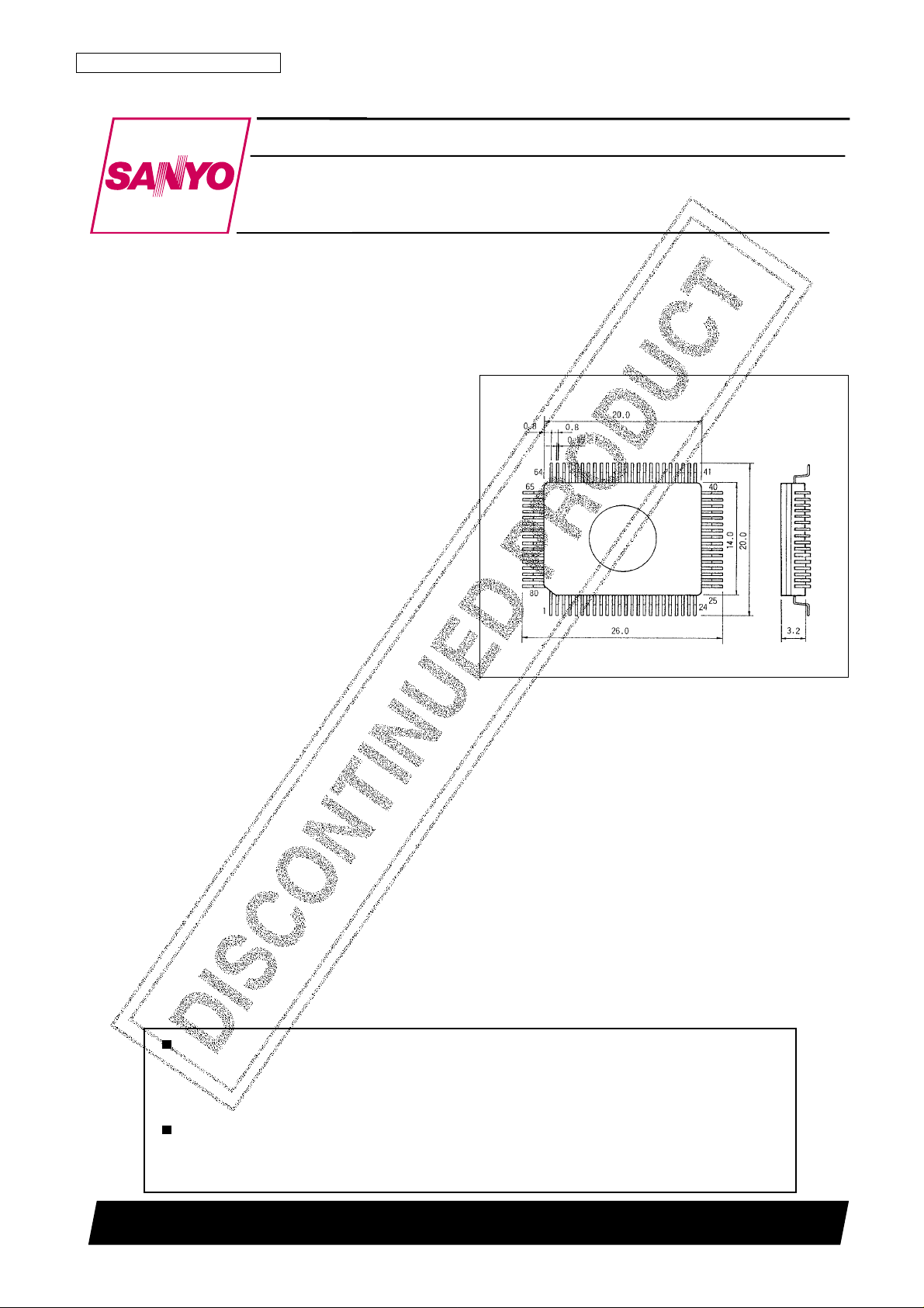
Package Dimensions
unit: mm
3152A-QFP80
Ordering number : EN*4741
83098HA (OT) / 83194 TH (OT) No. 4741-1/15
Preliminary
LC72E32
SANYO Electric Co.,Ltd. Semiconductor Bussiness Headquarters
TOKYO OFFICE Tokyo Bldg., 1-10, 1 Chome, Ueno, Taito-ku, TOKYO, 110-8534 JAPAN
Single Chip Microcontroller Plus PLL LSI
with On-Chip UVEPROM
CMOS LSI
Any and all SANYO products described or contained herein do not have specifications that can handle
applications that require extremely high levels of reliability, such as life-support systems, aircraft’s
control systems, or other applications whose failure can be reasonably expected to result in serious
physical and/or material damage. Consult with your SANYO representative nearest you before using
any SANYO products described or contained herein in such applications.
SANYO assumes no responsibility for equipment failures that result from using products at values that
exceed, even momentarily, rated values (such as maximum ratings, operating condition ranges, or other
parameters) listed in products specifications of any and all SANYO products described or contained
herein.
[LC72E32]
SANYO: QIP80
Page 2
Allowable Operating Ranges at Ta = 10 to 40°C, VDD= 3.5 to 5.5 V
No. 4741-2/15
LC72E32
Parameter Symbol Conditions
Ratings
Unit
min typ max
V
DD
1 CPU and PLL operating 4.5 5.5 V
Supply voltage V
DD
2 CPU operating 3.5 5.5 V
V
DD
3 Memory retention voltage 1.3 5.5 V
V
IH
1 G port 0.7 V
DD
8.0 V
V
IH
2 RES, INT, HOLD 0.8 V
DD
8.0 V
Input high level voltage
V
IH
3 SNS 2.5 8.0 V
V
IH
4 A port 0.6 V
DD
V
DD
V
V
IH
5 E and F ports 0.7 V
DD
V
DD
V
V
IH
6 LCTR (period measurement), VDD1 0.8 V
DD
V
DD
V
V
IL
1 G port 0 0.3 V
DD
V
V
IL
2 RES, INT 0 0.2 V
DD
V
V
IL
3 SNS 0 1.3 V
Input low level voltage V
IL
4 A port 0 0.2 V
DD
V
V
IL
5 E and F ports 0 0.3 V
DD
V
V
IL
6 LCTR (period measurement), VDD1 0 0.2 V
DD
V
V
IL
7 HOLD 0 0.4 V
DD
V
f
IN
1 XIN 4.0 4.5 5.0 MHz
f
IN
2 FMIN, VIN2, VDD1 10 130 MHz
f
IN
3 FMIN, VIN3, VDD1 10 150 MHz
Input frequency
f
IN
4 AMIN (L), VIN4, VDD1 0.5 10 MHz
f
IN
5 AMIN (H), VIN5, VDD1 2.0 40 MHz
f
IN
6 HCTR, VIN6, VDD1 0.4 12 MHz
f
IN
7 LCTR (frequency), VIN7, VDD1 100 500 kHz
f
IN
8 LCTR (period), VIH6, VIL6, VDD1 1 20 × 10
3
Hz
V
IN
1 XIN 0.50 1.5 Vrms
V
IN
2 FMIN 0.10 1.5 Vrms
Input amplitude V
IN
3 FMIN 0.15 1.5 Vrms
V
IN
4, 5 AMIN 0.10 1.5 Vrms
V
IN
6, 7 LCTR, HCTR 0.10 1.5 Vrms
Input voltage range V
IN
8 ADI 0 V
DD
V
Specifications
Absolute Maximum Ratings at Ta = 25°C, VSS= 0 V
Note: There are circuits in this IC with reduced resistance to damage from static electricity. Thus special care is required when handling this product.
Parameter Symbol Conditions Ratings Unit
Maximum supply voltage V
DD
max –0.3 to +6.5 V
Input voltage
V
IN
1 HOLD, INT, RES, ADI, SNS, and the G port –0.3 to +13 V
V
IN
2 Inputs other than VIN1 –0.3 to VDD+ 0.3 V
Output voltage
V
OUT
1 H port –0.3 to +15 V
V
OUT
2 Outputs other than V
OUT
1 –0.3 to VDD+ 0.3 V
I
OUT
1 All D and H port pins 0 to 5 mA
Output current
I
OUT
2 All E and F port pins 0 to 3 mA
I
OUT
3 All B and C port pins 0 to 1 mA
I
OUT
4 S1 to S28 and all I port pins 0 to 1 mA
Allowable power dissipation Pd max Topg = 10 to 40°C 400 mW
Operating temperature Topr 10 to 40 °C
Storage temperature Tstg –45 to +125 °C
Page 3
Electrical Characteristics for the Allowable Operating Ranges
No. 4741-3/15
LC72E32
Parameter Symbol Conditions
Ratings
Unit
min typ max
Hysteresis V
H
LCTR (period), RES, INT 0.1 V
DD
V
Rejected pulse width P
REJ
SNS 50 µs
Power-down detection voltage V
DET
3.0 3.5 4.0 V
I
IH
1
INT, HOLD, RES, ADI, SNS,
3.0 µA
and G port: V
I
= 5.5 V
I
IH
2
A, E, and F ports: E and F ports with
3.0 µA
Input high level current
outputs off, A port with no R
PD
, VI= V
DD
IIH3 XIN: VI= VDD= 5.0 V 2.0 5.0 15 µA
I
IH
4
FMIN, AMIN, HCTR, LCTR:
4.0 10 30 µA
V
I
= VDD= 5.0 V
I
IH
5 A port: With an RPD, VI= VDD= 5.0 V 50 µA
I
IL
1
INT, HOLD, RES, ADI, SNS,
3.0 µA
and G port: V
I
= V
SS
Input low level current
I
IL
2
A, E, and F ports: E and F ports with
3.0 µA
outputs off, A port with no R
PD
, VI= V
SS
IIL3 XIN: VIN= V
SS
2.0 5.0 15 µA
I
IL
4 FMIN, AMIN, HCTR, LCTR: VI= V
SS
4.0 10 30 µA
Input floating voltage V
IF
A port: With an R
PD
0.05 V
DD
V
Pull-down resistance R
PD
A port: With an RPD, VDD= 5.0 V 75 100 200 kΩ
I
OFFH
1 EO1, EO2: VO= V
DD
0.01 10 nA
Output high level off leakage current I
OFFH
2 B, C, D, E, F, and I ports: VO= V
DD
3.0 µA
I
OFFH
3 H port: VO= 13 V 5.0 µA
Output low level off leakage current
I
OFFL
1 EO1, EO2: VO= V
SS
0.01 10 nA
I
OFFL
2 B, C, D, E, F, and I ports: VO= V
DD
3.0 µA
V
OH
1 B and C ports: IO= 1 mA VDD– 2.0 VDD– 1.0 VDD– 0.5 V
V
OH
2 E and F ports: IO= 1 mA VDD– 1.0 V
V
OH
3 EO1, EO2: IO= 500 µA VDD– 1.0 V
Output high level voltage V
OH
4 XOUT: IO= 200 µA VDD– 1.0 V
V
OH
5 S1 to S28 and I port: IO= –0.1 mA VDD– 1.0 V
V
OH
6 D port: IO= 5 mA VDD– 1.0 V
V
OH
7 COM1 and COM2: IO= 25 µA VDD– 0.75 VDD– 0.5 VDD– 0.3 V
V
OL
1 B and C ports: IO= 50 µA 0.5 1.0 2.0 V
V
OL
2 E and F ports: IO= 1 mA 1.0 V
V
OL
3 EO1, EO2: IO= 500 µA 1.0 V
Output low level voltage
V
OL
4 XOUT: IO= 200 µA 1.0 V
V
OL
5 S1 to S28 and I port: IO= 0.1 mA 1.0 V
V
OL
6 D port: IO= 5 mA 1.0 V
V
OL
7 COM1, COM2: IO= 25 µA 0.3 0.5 0.75 V
V
OL
8 H port: IO= 5 mA (150 Ω) 0.75 (400 Ω) 2.0 V
Output middle level voltage V
M
1 COM1, COM2: VDD= 5.0 V, IO= 20 µA 2.0 2.5 3.0 V
A/D conversion error ADI: V
DD
1 –1/2 1/2 LSB
I
DD
1VDD1, fIN2 = 130 MHz 15 20 mA
I
DD
2
V
DD
= 5.0 V, PLL stopped, CT = 2.67 µs
2.7 mA
(HOLD mode, Figure 1)
I
DD
3
V
DD
= 5.0 V, PLL stopped, CT = 13.33 µs
1.7 mA
(HOLD mode, Figure 1)
Current drain
I
DD
4
V
DD
= 5.0 V, PLL stopped, CT = 40.00 µs
1.5 mA
(HOLD mode, Figure 1)
V
DD
= 5.5 V, oscillator stopped, Ta = 25°C
5µA
I
DD
5
(BACK UP mode, Figure 2)
V
DD
= 2.5 V, oscillator stopped, Ta = 25°C
1µA
(BACK UP mode, Figure 2)
Page 4
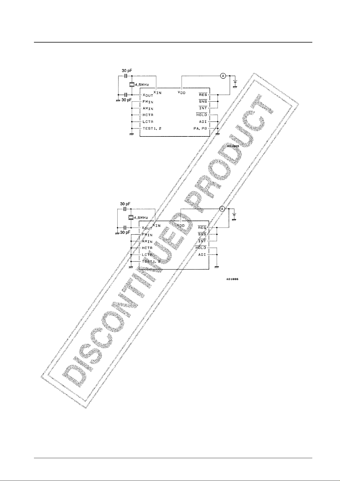
Test Circuits
Note: PB to PF, PH, and PI are all open. However, PE and PF are output-selected.
Figure 1 IDD2 to IDD4 in HOLD Mode
Note: PA to PI, S1 to S24, COM1, and COM2 are all open.
Figure 2 IDD5 in BACK UP Mode
No. 4741-4/15
LC72E32
Page 5
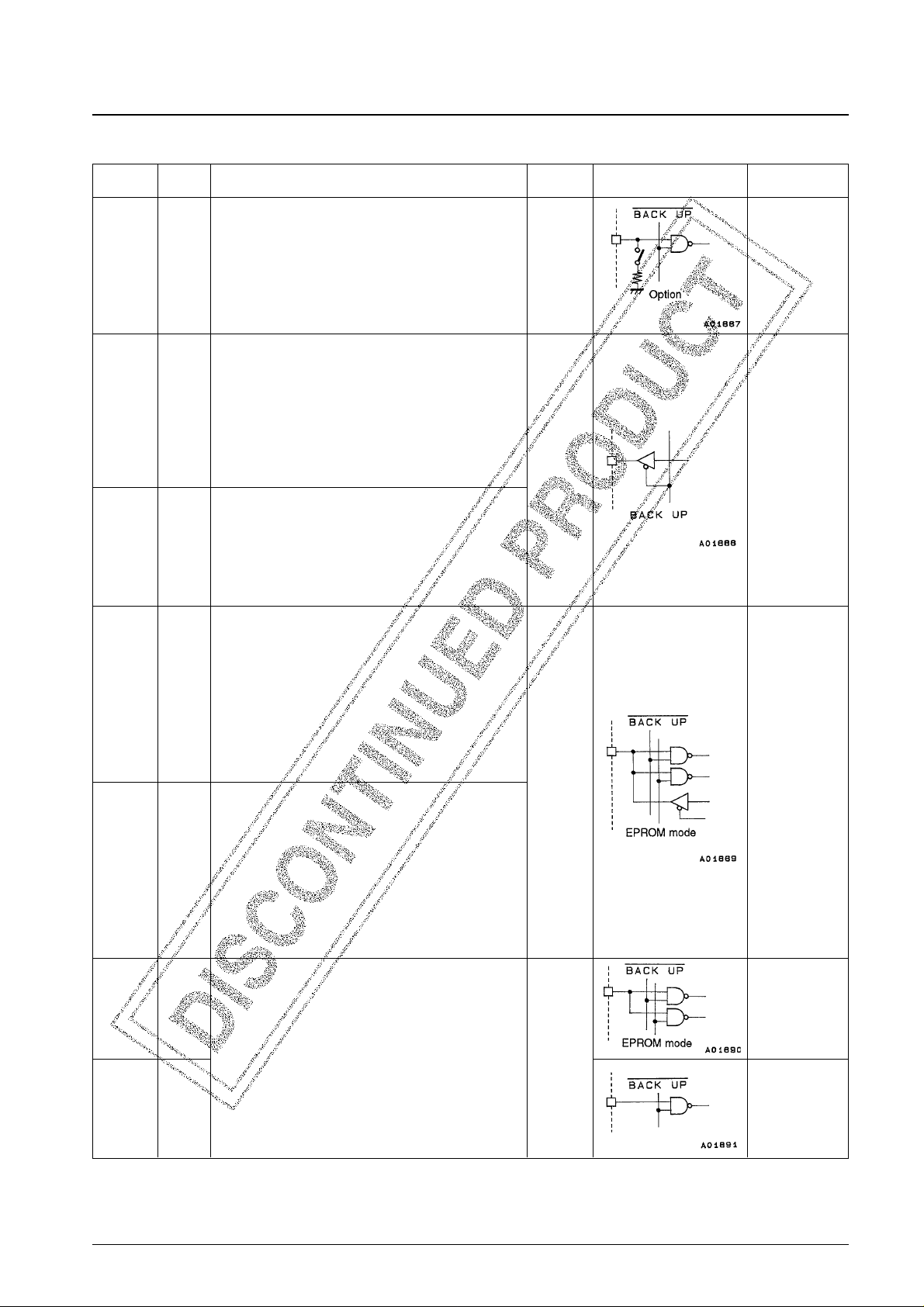
Pin Functions
No. 4741-5/15
LC72E32
Pin Pin No. Function I/O I/O circuit type
EPROM mode
function
PA0
PA1
PA2
PA3
PB0
PB1
PB2
PB3
PC0
PC1
PC2
PC3
PD0
PD1
PD2
PD3
PE0
PE1
PE2
PE3
PF0
PF1
PF2
PF3
PG0
PG1
PG2
PG3
35
34
33
32
30
29
28
27
26
25
24
23
22
21
20
19
18
17
16
15
14
13
12
11
6
5
4
3
Low threshold type dedicated input port
These pins can be used, for example, for key data acquisition.
Built-in pull-down resistors can be specified as an option. This
option is in 4-pin units, and cannot be specified for individual
pins.
Input through these pins is disabled in BACKUP mode.
Dedicated output ports
Since the output transistor impedances are unbalanced
CMOS, these pins can be effectively used for functions such
as key scan timing. These pins go to the output high
impedance state in BACKUP mode.
These pins go to the low level during a reset, i.e., when the
RES pin is low.
Dedicated output port
These are normal CMOS outputs. These pins go to the output
high impedance state in BACKUP mode.
These pins go to the low level during a reset, i.e., when the
RES pin is low.
I/O port
These pins are switched between input and output as follows.
Once an input instruction (IN, TPT, or TPF) is executed, these
pins latch in the input mode. Once an output instruction (OUT,
SPB, or RPB) is executed, they latch in the output mode.
These pins go to the input mode during a reset, i.e., when the
RES pin is low.
In BACKUP mode these pins go to the input mode with input
disabled.
I/O port
These pins are switched between input and output by the
FPC instruction.
The I/O states of this port can be specified for individual pins.
These pins go to the input mode during a reset, i.e., when the
RES pin is low.
In BACKUP mode these pins go to the input mode with input
disabled.
Dedicated input port
Input through these pins is disabled in BACKUP mode.
Input
Output
I/O
Input
Data I/O
PE0: D0
PE1: D1
PE2: D2
PE3: D3
PF0: D4
PF1: D5
PF2: D6
PF3: D7
EPROM control
signal inputs
PG0: CE
PG1: OE
Continued on next page.
Page 6
Continued from preceding page.
No. 4741-6/15
LC72E32
Pin Pin No. Function I/O I/O circuit type
EPROM mode
function
PH0
PH1
PH2
PH3
PI0/S25
PI1/S26
PI2/S27
PI3/S28
S1 to S14
S15 to S24
COM1
COM2
FMIN
AMIN
10
9
8
7
39
38
37
36
63 to 50
49 to 40
65
64
74
75
Dedicated output port
Since these pins are high breakdown voltage n-channel
transistor open-drain outputs, they can be effectively used for
functions such as band power supply switching.
Note that PH2 and PH3 also function as the DAC1 and DAC2
outputs.
These pins go to the high impedance state during a reset, i.e.,
when the RES pin is low, and in BACKUP mode.
Dedicated output port
While these pins have a CMOS output circuit structure, they
can be switched to function as LCD drivers. Their function is
switched by the SS and RS instructions. These pins cannot
be switched individually.
The LCD driver function is selected and a segment off signal
is output when power is first applied or when RES is low.
These pins are held at the low level in BACKUP mode.
Note that when the general-purpose port use option is
specified, these pins output the contents of IPORT when LPC
is 1, and the contents of the general-purpose output port
LATCH when LPC is 0.
LCD driver segment outputs
A frame frequency of 100 Hz and a 1/2 duty, 1/2 bias drive
type are used.
A segment off signal is output when power is first applied or
when RES is low.
These pins are held at the low level in BACKUP mode.
The use of these pins as general-purpose output ports can be
specified as an option.
LCD driver common outputs
A 1/2 duty, 1/2 bias drive type is used.
The output when power is first applied or when RES is low is
identical to the normal operating mode output.
These pins are held at the low level in BACKUP mode.
FM VCO (local oscillator) input
The input must be capacitor-coupled.
The input frequency range is from 10 to 130 MHz.
AM VCO (local oscillator) input
The band supported by this pin can be selected using the PLL
instruction.
High (2 to 40 MHz) → SW
Low (0.5 to 10 MHz) → LW and MW
Output
Output
I/O
Output
Output
Input
Address input
S1: A0 to
S14: A13
Continued on next page.
Page 7

Continued from preceding page.
No. 4741-7/15
LC72E32
Pin Pin No. Function I/O I/O circuit type
EPROM mode
function
HCTR
LCTR
ADI
INT
EO1
EO2
SNS
HOLD
RES
XIN
XOUT
TEST1
TEST2
V
DD
V
SS
70
71
69
66
77
78
72
67
68
1
80
79
2
31, 73
76
Universal counter input
The input should be capacitor-coupled.
The input frequency range is from 0.4 to 12 MHz.
This input can be effectively used for FM IF or AM IF
counting.
Universal counter input
The input should be capacitor-coupled for input frequencies in
the range 100 to 150 kHz.
Capacitor coupling is not required for input frequencies from
1 to 20 Hz.
This input can be effectively used for AM IF counting.
A/D converter input
A 1.28 ms period is required for a 6-bit sequential comparison
conversion. The full scale input is ((63/96) · V
DD
) for a data
value of 3FH.
Interrupt request input
An interrupt is generated when the INTEN flag is set (by an
SS instruction) and a falling edge is input.
Reference frequency and programmable divisor phase
comparison error outputs
Charge pump circuits are built in.
EO1 and EO2 are the same.
Input pin used to determine if a power outage has occurred in
BACKUP mode
This pin can also be used as a normal input port.
Input pin used to force the LC72E32 to HOLD mode
The LC72E32 goes to HOLD mode when the HOLDEN flag is
set (by an SS instruction) and the HOLD input goes low.
A high breakdown voltage circuit is used so that this input can
be used in conjunction with the normal power switch.
System reset input
This signal should be held low for 75 ms after power is first
applied to effect a power-up reset.
The reset starts when a low level has been input for at least
six reference clock cycles.
Crystal oscillator connections
(4.5 MHz)
A feedback resistor is built in.
LSI test pins. These pins must be connected to V
SS
.
Power supply + connections. Both pins must be connected.
Power supply – connection.
Input
Input
Input
Output
Input
Input
Input
Input
Output
EPROM write
power
Vpp
Page 8

Option
Usage Notes
The LC72E32 is provided for development of LC7232N application programs and for LC7232N function evaluation.
The points listed below required attention when using the LC72E32.
1. Differences between the LC72E32 and the LC7232N
Note: * This refers to the option setup time of about 1 ms that occurs following the period of about 75 ms from power application.
2. PLA and options
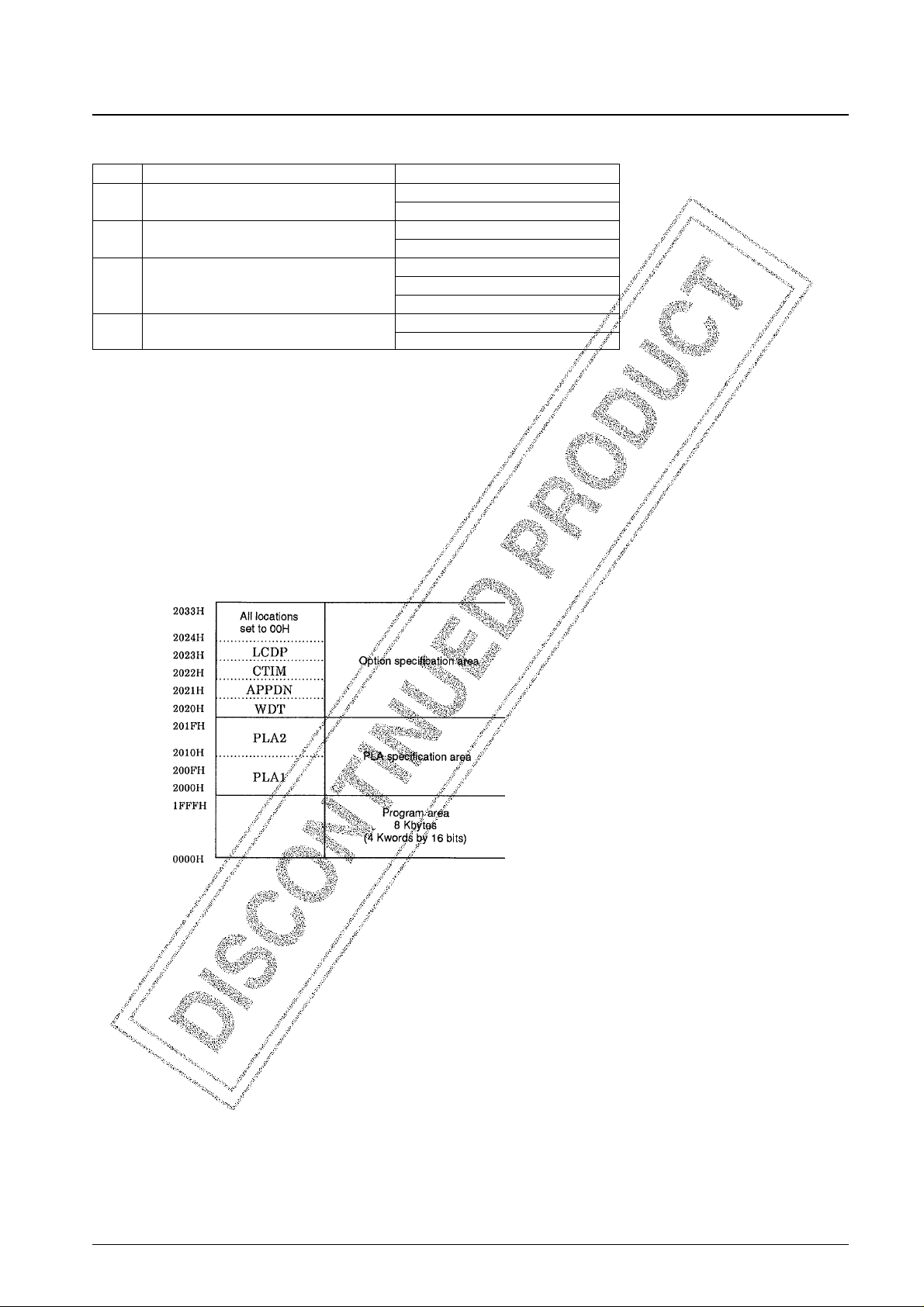
The LC72E32 uses location 2000H to 201FH as program memory for PLA pattern specification, and locations
2020H to 2033H for option specification. This option specification allows the LC72E32 to support option setups
identical to those available with the LC7232N.
No. 4741-8/15
LC72E32
Item LC72E32 LC7232N
Operating temperature (Topr) 10 to 40 °C –40 to +85°C
After the 75 ms power on reset period, the LSI internal
Operation immediately option settings are set up during a period of about 1 ms. After the 75 ms power on reset period, program execution
following power on After that operation completes, program execution starts starts with the program counter set to location 0.
with the program counter set to location 0.
Input type of the A port
No pull-down resistors
Pull-down resistors are included or not according to the
immediately following power on* option specifications.
Output type of the S1 to S28 These pins function as either LCD ports or general-
outputs immediately following LCD ports purpose output ports according to the option
power on* specifications.
Power-down detection voltage
Minimum: 3.0 V Minimum: 2.7 V
(V
DET
)
Typical: 3.5 V Typical: 3.0 V
Maximum: 4.0 V Maximum: 3.3 V
Conditions: V
DD
= 5.0 V, PLL stopped Conditions: VDD2, PLL stopped
I
DD
2 CT = 2.67 µs (HOLD mode, Figure 1) CT = 2.67 µs (HOLD mode, Figure 1)
Typical: 2.7 mA Typical: 1.5 mA
Conditions: VDD= 5.0 V, PLL stopped Conditions: VDD2, PLL stopped
Current drain I
DD
3 CT = 13.33 µs (HOLD mode, Figure 1) CT = 13.33 µs (HOLD mode, Figure 1)
Typical: 1.7 mA Typical: 1.0 mA
Conditions: V
DD
= 5.0 V, PLL stopped Conditions: VDD2, PLL stopped
I
DD
4 CT = 40.00 µs (HOLD mode, Figure 1) CT = 40.00 µs (HOLD mode, Figure 1)
Typical: 1.5 mA Typical: 0.7 mA
The TEST1 and TEST2 pins These are LSI test pins and must be connected to V
SS
.
These are LSI test pins and must be either left open or
connected to V
SS
.
No. Description Selections
1 WDT (watchdog timer) inclusion selection
WDT included
No WDT
2 Port A pull-down resistor inclusion selection
Pull-down resistors included
No pull-down resistors
2.67 µs
3 Cycle time selection 13.33 µs
40.00 µs
4 LCD port/general-purpose port selection
LCD ports
General-purpose output ports
Page 9
LC72E32 Option Types
Note that these options are not determined until the option setting period of about 1 ms, which follows a period of about
75 ms from power application, has passed.
3. Use of the mass produced unit printed circuit board
When using the printed circuit board for the massed produced end product with the LC72E32, be sure to connect the
TEST1 and TEST2 pins to V
SS
and be sure to connect both pins 31 and 73 (the VDDpins) to the plus side of the
power supply.
4. EPROM address space
Note: Due to their structure, on-chip EPROM microcontrollers (products in which the EPROM has not been written)
cannot be fully tested prior to shipment. As a result, the yield after writing may be decreased.
No. 4741-9/15
LC72E32
Symbol Option Type Selections
WDT WDT (watchdog timer) inclusion selection
WDT included
No WDT
APPDN A port pull-down resistor inclusion selection
Pull-down resistors included
No pull-down resistors
2.67 µs
CTIM Cycle time selection 13.33 µs
40.00 µs
LCDP LCD port/general-purpose port selection
LCD ports
General-purpose output ports
Page 10

Usage Techniques
1. Writing the on-chip EPROM
There are two techniques that can be used to write to the LC72E32’s on-chip EPROM.
• Use of a general-purpose EPROM programmer
The LC72E32’s EPROM can be written using a general-purpose EPROM programmer. This requires the use of a
special-purpose adapter, the LC72E32 Adapter for EPROM Programmer. Use the Intel 27512 (Vpp = 12.5 V)
high-speed writing technique, and specify the address settings as locations 0 to 2033H.
• Use of the RE32 in-circuit emulator
The LC72E32’s EPROM can be written using the RE32 in-circuit emulator. This requires the use of a specialpurpose adapter, the LC72E32 Adapter for RE32. Use the PGOTP command as the writing technique.
2. Special-purpose EPROM writing adapters
As mentioned above, there are two EPROM writing techniques, each of which requires the use of the appropriate
adapter.
Note: The external dimensions of these two adapters are essentially identical.
General-purpose EPROM programmer adapter:
Product name: LC72E32 Adapter for EPROM Programmer
Product code: NDK-DC-001-A
RE32 in-circuit emulator adapter:
Product name: LC72E32 Adapter for RE32
Product code: NDK-DC-003-A
• Erasure
Use a general-purpose EPROM eraser to erase written data.
• Light Seal
The LC72E32 includes UVEPROM, i.e., ultraviolet erasable EPROM. When actually using an LC72E32, its
window should be covered with UV-opaque tape.
No. 4741-10/15
LC72E32
Page 11

Pin Assignment
No. 4741-11/15
LC72E32
Top view
Page 12

Block Diagram
No. 4741-12/15
LC72E32
Page 13

LC72E32 Instruction Table
Abbreviations:
ADDR: Program memory address [12 bits]
b: Borrow
B: Bank number [2 bits]
C: Carry
DH: Data memory address high (row address) [2 bits]
DL: Data memory address low (column address) [4 bits]
I: Immediate data [4 bits]
M: Data memory address
N: Bit position [4 bits]
Pn: Port number [4 bits]
r: General register (one of the locations 00 to 0FH in bank 0)
Rn: Register number [4 bits]
( ): Contents of register or memory
( )n: Contents of bit N of register or memory
No. 4741-13/15
LC72E32
Mnemonic
Operand
Function Operation
Machine code
1st 2nd D15141312111098 7654 321D0
AD r M Add M to r r ← (r) + (M) 010000 DH DL Rn
ADS r M
Add M to r, r ← (r) + (M)
0100 01 DH DL Rn
then skip if carry skip if carry
AC r M Add M to r with carry r ← (r) + (M) + C 0100 10 DH DL Rn
ACS r M
Add M to r with carry, r ← (r) + (M) + C
0100 11 DH DL Rn
then skip if carry skip if carry
AI M I Add I to M M ← (M) + I 0101 00 DH DL I
AIS M I
Add I to M, M ← (M) + I
0101 01 DH DL I
then skip if carry skip if carry
AIC M I Add I to M with carry M ← (M) + I + C 0101 10 DH DL I
AICS M I
Add I to M with carry, M ← (M) + I + C
0101 11 DH DL I
then skip if carry skip if carry
SU r M Subtract M from r r ← (r) – (M) 0110 00 DH DL Rn
SUS r M
Subtract M from r, r ← (r) – (M)
0110 01 DH DL Rn
then skip if borrow skip if borrow
SB r M
Subtract M from r with
r ← (r) – (M) – b 0110 10 DH DL Rn
borrow
Subtract M from r with
r ← (r) – (M) – b
SBS r M borrow,
skip if borrow
0110 11 DH DL Rn
then skip if borrow
SI M I Subtract I from M M ← (M) – I 0111 00 DH DL I
SIS M I
Subtract I from M, M ← (M) – I
0111 01 DH DL I
then skip if borrow skip if borrow
SIB M I
Subtract I from M with
M ← (M) – I – b 0111 10 DH DL I
borrow
Subtract I from M with
M ← (M) – I – b
SIBS M I borrow,
skip if borrow
0111 11 DH DL I
then skip if borrow
SEQ r M Skip if r equals M
r – M
0000 01 DH DL Rn
skip if zero
Skip if r is greater
r – M
SGE r M
than or equal to M
skip if not borrow 0000 11 DH DL Rn
(r) ≥ (M)
SEQI M I Skip if M equal to I
M – I
0011 01 DH DL I
skip if zero
Skip if M is greater
M – I
SGEI M I
than or equal to I
skip if not borrow 0011 11 DH DL I
(M) ≥ I
Instruction
Group
Addition instructionsSubtraction instructions
Comparison instructions
Continued on next page.
Page 14

Continued from preceding page.
No. 4741-14/15
LC72E32
Mnemonic
Operand
Function Operation
Machine code
1st 2nd D15141312111098 7654 321D0
AND M I AND I with M M ← (M)I 0011 00 DH DL I
OR M I OR I with M M ← (M)I 0011 10 DH DL I
EXL r M Exclusive OR M with r r ← (r)(M) 0010 00 DH DL Rn
LD r M Load M to r r ← (M) 1000 00 DH DL Rn
ST M r Store r to M M ← (r) 1000 01 DH DL Rn
Move M to destination
MVRD r M M referring to r in [DH, Rn] ← (M) 1000 10 DH DL Rn
the same row
Move source M
MVRS M r referring to r to M in M ← [DH, Rn] 1000 11 DH DL Rn
the same row
MVSR M1 M2
Move M to M in
[DH, DL1] ← [DH, DL2] 1001 00 DH DL1 DL2
the same row
MVI M I Move I to M M ← I 1001 01 DH DL I
PLL M r
Load M to PLL
PLL r ← PLL DATA 1001 10 DH DL Rn
registers
Test M bits, then skip
if M (N) = all 1s,
TMT M N if all bits specified
then skip
1010 01 DH DL N
are true
Test M bits, then skip
if M (N) = all 0s,
TMF M N if all bits specified
then skip
1010 11 DH DL N
are false
JMP ADDR Jump to the address PC ← ADDR 1011 ADDR (12 bits)
PC ← ADDR
CAL ADDR Call subroutine
Stack ← (PC) + 1
1100 ADDR (12 bits)
RT Return from subroutine PC ← Stack 1101 01000000 000 0
RTI Return from interrupt PC ← Stack 1101 01010000 000 0
Test timer F/F
if timer F/F = 0,
TTM N then skip if it has
then skip
1101 01100000 N
not been set
Test unlock F/F
if UL F/F = 0,
TUL N then skip if it has
then skip
1101 01110000 N
not been set
SS N Set status register
(Status register 1)
1101 11000000 N
N ← 1
RS N Reset status register
(Status register 1)
1101 11010000 N
N ← 0
TST N Test status register true
if (Status register 2) N =
1101 11100000 N
all 1s, then skip
TSF N Test status register false
if (Status register 2) N =
1101 11110000 N
all 0s, then skip
BANK B Select bank BANK ← B 1101 00 B 0000 000 0
Instruction
Group
Logical operation
instructions
Transfer instructions
Bit test
instructions
Jump and subroutine
call instructions
F/F test
instructions
Status register instructions
Bank switching
instructions
Continued on next page.
Page 15

PS No. 4741-15/15
LC72E32
This catalog provides information as of September, 1998. Specifications and information herein are
subject to change without notice.
Specifications of any and all SANYO products described or contained herein stipulate the performance,
characteristics, and functions of the described products in the independent state, and are not guarantees
of the performance, characteristics, and functions of the described products as mounted in the customer’s
products or equipment. To verify symptoms and states that cannot be evaluated in an independent device,
the customer should always evaluate and test devices mounted in the customer’s products or equipment.
SANYO Electric Co., Ltd. strives to supply high-quality high-reliability products. However, any and all
semiconductor products fail with some probability. It is possible that these probabilistic failures could
give rise to accidents or events that could endanger human lives, that could give rise to smoke or fire,
or that could cause damage to other property. When designing equipment, adopt safety measures so
that these kinds of accidents or events cannot occur. Such measures include but are not limited to protective
circuits and error prevention circuits for safe design, redundant design, and structural design.
In the event that any or all SANYO products (including technical data, services) described or contained
herein are controlled under any of applicable local export control laws and regulations, such products must
not be exported without obtaining the export license from the authorities concerned in accordance with the
above law.
No part of this publication may be reproduced or transmitted in any form or by any means, electronic or
mechanical, including photocopying and recording, or any information storage or retrieval system,
or otherwise, without the prior written permission of SANYO Electric Co., Ltd.
Any and all information described or contained herein are subject to change without notice due to
product/technology improvement, etc. When designing equipment, refer to the “Delivery Specification”
for the SANYO product that you intend to use.
Information (including circuit diagrams and circuit parameters) herein is for example only; it is not
guaranteed for volume production. SANYO believes information herein is accurate and reliable, but
no guarantees are made or implied regarding its use or any infringements of intellectual property rights
or other rights of third parties.
Continued from preceding page.
Mnemonic
Operand
Function Operation
Machine code
1st 2nd D15141312111098 7654 321D0
LCD M I
Output segment pattern
LCD (DIGIT) ← M 1110 00 DH DL DIGIT
to LCD digit direct
LCP M I
Output segment pattern
LCD (DIGIT) ← PLA ← M 1110 01 DH DL DIGIT
to LCD digit through PLA
IN M P Input port data to M M ← (Port (P)) 1110 10 DH DL P
OUT M P Output contents of M to port (Port (P)) ← M 1110 11 DH DL P
SPB P N Set port bits (Port (P)) N ← 1 1111 0000 P N
RPB P N Reset port bits (Port (P)) N ← 0 1111 0101 P N
Test port bits, if (Port (P)) N = all 1s,
TPT P N then skip if all bits then skip 1111 1010 P N
specified are true
Test port bits, if (Port (P)) N = all 0s,
TPF P N then skip if all bits then skip 1111 1111 P N
specified are false
UCS I Set I to UCCW1 UCCW1 ← I 0000 00010000 I
UCC I Set I to UCCW2 UCCW2 ←I 0000 00110000 I
FPC N F port I/O control FPC latch ← N 000100000000 N
CKSTP Clock stop Stop clock if HOLD = 0 0001 00010000 000 0
DAC I Load M to D/A registers DAreg ←DAC DATA 0000 00100000 I
NOP No operation 0000 00000000 000 0
Instruction
Group
I/O instruction Group
Universal counter
instructions
Other
instructions
 Loading...