

Page 1
Any and all SANYO products described or contained herein do not have specifications that can handle
applications that require extremely high levels of reliability, such as life-support systems, aircraft’s
control systems, or other applications whose failure can be reasonably expected to result in serious
physical and/or material damage. Consult with your SANYO representative nearest you before using
any SANYO products described or contained herein in such applications.
SANYO assumes no responsibility for equipment failures that result from using products at values that
exceed, even momentarily, rated values (such as maximum ratings, operating condition ranges,or other
parameters) listed in products specifications of any and all SANYO products described or contained
herein.
CMOS IC
Single-chip PLL and Microcontroller
with LCD Driver
Ordering number:ENN*4350
LC7234-8460
SANYO Electric Co.,Ltd. Semiconductor Company
TOKYO OFFICE Tokyo Bldg., 1-10, 1 Chome, Ueno, Taito-ku, TOKYO, 110-8534 JAPAN
Preliminary
Overview
The LC7234-8460 is a single-chip microcontroller that incorporates a phase-locked loop (PLL) and a liquid crystal
display driver.
The LC7234-8460 operates over the American, European,
Chinese, Middle Eastern, Canadian and Australian LW,
MW, SW and FM bands, and incorporates preset-channel
memory, automatic or manual tuning, high-speed station
search, and clock and timer functions.
The LC7234-8460 operates from a 5 V supply and is a v ailable in 64-pin QIPs.
Features
• Operates over the LW, MW, SW1, SW2 and FM bands.
• Three selectable preset memory configurations.
• Automatic tuning or manual preset memory scan.
• High-speed station search.
FM band: 60 ms per step.
AM band: 70 ms per step.
• Clock function.
• ON, OFF and SLEEP timer functions.
• Logic-level and momentary switch band select inputs.
• LCD display with wide viewing angle and high contrast
over a wide operating temperature range.
• On-chip amplifier for external lowpass filter.
• External RC network for reset not required.
• Forced mono mode.
• High signal-to-noise ratio.
• Single 5 V supply.
• 64-pin QIPs.
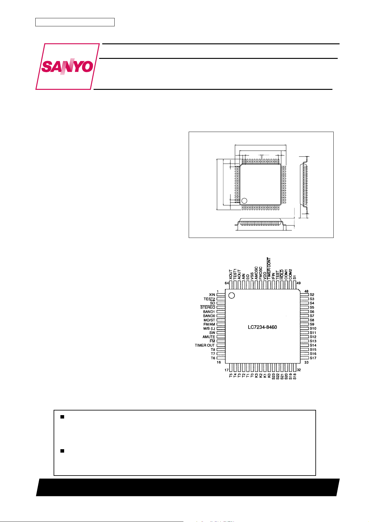
Package Dimensions
unit:mm
3159-QIP64E
[LC7234-8460]
17.2
14.0
0.8
0.35
15.6
17.2
1.6
14.0
1.0
48
1.0
49
0.8
64
1.0
1
Pin Assignment
1.6
1.0
33
32
17
16
0.8
SANYO : QIP64E
3.0max
0.15
0.1
2.7
Top view
O1501TN (KT)/32693JN No.4350–1/23
Page 2
Pin Function
1NIX.noitcennoctupnirotallicsolatsyrczHM5.4
22TSET.DNGotdetcennocyllamroN.tupnitseT
3DS
4OERETS
51DNAB
60DNAB
7TS/OM
8MA/MF
9)L(S/M
01WS
11ETUMA
21MF
31TUOREMIT
71ot415Tot8T
22ot810Tot4T
62ot320Kot3KVottcennoC.stupninacsyekHGIH-evitcA
94ot721Sot32S.esunitonnehwnepoevaeL.stuptuorevirdtnemgeS
15,051MOC,2MOC .esunitonnehwnepoevaeL.stuptuorevirdnommoC
25DLOH
35TSET .noitamrofnirehtrufrofnoitpircsedyektseTehteeS.tupnitsetHGIH-evitcA
45NIFIVottcennoC.tupnilangisFIMF/MA
55TNOCREMIT
65VDDylppusV5
75CSOMFVottcennoC.tupnirotallicsolacolMF
85CSOMAVottcennoC.tupnirotallicsolacolMA
95VSSdnuorG
06OE.tuptuorotarapmocesahP
16NIAVottcennoC.noitcennoctupnireifilpmaretlifssapwoL
26TUOAVottcennoC.noitcennoctuptuoreifilpmaretlifssapwoL
361TSET.DNGotdetcennocyllamroN.tupnitseT
46TUOX.noitcennoctuptuorotallicsolatsyrczHM5.4
LC7234-8460
rebmuNemaNnoitpircseD
VottcennoC
SS
VottcennoC
DD
.esunitonnehw
VottcennoC
DD
.esunitonnehw
.esunitonnehw
.esunitonnehwnepoevaeL.teserretfa
.esunitonnehwnepoevaeL.teser
.esunitonnehwnepoevaeL.teserretfa
.esunitonnehwnepoevaeL
.esunitonnehwnepoevaeL.teser
I(detcelessiedomdloh,gnitarepo
DD
SS
.esunitonnehw
SS
SS
.detcetedsinoitatsanehwevitcasitupnisiht,gninutotuagniruD.tupnitcetednoitatsWOL-evitcA
.NOsiDELyalpsidOERETSeht,edomMFgnirudWOLnehW.tupnitcetedoeretsWOL-evitcA
.selbattcelesdnabehteeS.0siDNBLESnehwevitcA.stupnitcelesdnaB
levelWOL.HGIHnehwoeretsdnaWOLnehwonoM.tuptuorotacidnioerets/onomHGIH-evitcA
retfalevelHGIH.HGIHnehwMFdnaWOLnehwMA.tuptuotcelesdnabMA/MFHGIH-evitcA
.esunitonnehwnepoevaeL.teserretfalevelWOL
.esunitonnehwnepoevaeL.teserretfalevelHGIH
SS
I(detcelessiedompukcab,gnitarepotonsikcolceht
.esusitonnehw
DD
.esunitonnehw
.esunitonnehw
.esunitonnehw
SS
SS
.).xamAµ5=
.esunitonnehw
.esunitonnehw
.WOLnehw)WL(WSdnaHGIHnehwWM.tuptuotcelesdnabevawtrohs/muidemWOL-evitcA
levelWOL.HGIHnehw2WSdnaWOLnehw1WS.tuptuotcelesdnabevawtrohsHGIH-evitcA
.ycneuqerfreviecergnignahcnehwtuptuooiduaehtstuC.tuptuolortnocetumoiduaHGIH-evitcA
.teserretfalevelWOL.HGIHnehwMAdnaWOLnehwMF.tuptuotcelesMF/MAHGIH-evitcA
retfalevelWOL.noitarepoedompeelsdnaremitgnirudHGIH.tuptuolortnocremitHGIH-evitcA
noitisnartHGIH-ot-WOLanehwdennacssixirtamehT.stuptuonacsxirtamedoidHGIH-evitcA
nepoevaeL.teserretfalevelWOL.degnahcsahatadfidezilaitinisieciveD.DLOHnosrucco
yekgnidnopserrocehtnehwylnodennacssixirtamyekehT.stuptuonacsxirtamyekHGIH-evitcA
.esunitonnehwnepoevaeL.teserretfalevelHGIH.nacshcaeretfaHGIHseoG.desserpsi
sikcolcehtdnasrucconoitisnartWOL-ot-HGIHanehW.tupnilortnocedomdlohWOL-evitcA
dnasrucconoitisnartWOL-ot-HGIHanehW.).pytAm7.0=
.HGIHnehwgnitarepotondnaWOLnehwgnitareporemiT.tupnilortnocremitWOL-evitcA
Specifications
Absolute Maximum Ratings at Ta = 25˚C, VSS = 0V
retemaraPlobmySsnoitidnoCsgnitaRtinU
egatlovylppuSV
egatlovtupnI
egatlovtuptuO
tnerructuptuO
noitapissidrewopelbawollAxamdP=aT– 58+ot04°C 004Wm
erutarepmetgnitarepOrpoT –58+ot04
erutarepmetegarotSgtsT –521+ot54
DD
V
1NI
V
2NI
V
1TUO
V
2TUO
I
1TUO
I
2TUO
I
3TUO
I
4TUO
1DNAB
TUOA
–5.6+ot3.0
,0DNAB,TNOCREMIT,OERETS,DS,TSET,DLOH
stupnirehtollA
TUOA,MA/MF,TS/OM
stuptuorehtollA
MA/MF,TS/OM
8Tot6T,TUOREMIT,MF,ETUMA,WS,)L(S/M
5Tot0T
–Vot3.0
–Vot3.0
–31+ot3.0
DD
–51+ot3.0
DD
V
V
3.0+
V
3.0+
5ot0
3ot0
Am
1ot0
2ot0
˚C
˚C
No.4350–2/23
Page 3
LC7234-8460
Reommended Operating Conditions at Ta = –40 to +85˚C, VDD = 3.5 to 5.5V
retemaraPlobmySsnoitidnoC
V
egatlovylppuS
egatlovlevel-hgihtupnI
egatlovlevel-woltupnI
ycneuqerftupnI
edutilpmatupnI
1DD
2DD
V
3DD
V
1HI
2HI
V
3HI
V
1LI
2LI
V
3LI
f
1NI
f
2NI
f
3NI
f
4NI
f
5NI
V
1NI
V
2NI
V
4,3NI
V
5NI
DLOHV8.0
DLOH0V4.0
NIX0.45.4
,CSOMFV
,NIFIV
5NI
NIX05.0
CSOMF01.0
CSOMA01.0
NIFI01.05.1
Electrical Characteristics Under recommended operating conditions
retemaraPlobmySsnoitidnoC
egatlovnoitcetednwod-rewoPV
terruclevel-hgihtupnI
terruclevel-woltupnI
egatlovgnitaolftupnIV
ecnatsisernwod-lluPR
tnerrucegakaelFFOtuptuO
egatlovlevel-hgihtuptuO
egatlovlevel-woltuptuO
TED
I
1HI
I
2HI
I
3HI
I
4HI
I
5HI
I
1LI
I
2LI
I
3LI
I
4LI
FI
VIV=
VIV=
VIV=
V:NIX
V:NIA
V:NIA
IV=DD
IV=DD
SS
SS
SS
IV=SS
3Kot0K
DP
I
I
I
I
I
I
V
1HO
V
2HO
V
3HO
V
4HO
V
5HO
V
6HO
V
1LO
V
2LO
V
3LO
V
4LO
V
5LO
V
6LO
V
7LO
V
8LO
V:OE
1HFFO
2HFFO
OV=DD
V:)L(S/M
3HFFO
V:OE
OV=SS
I:OE
O
I:OE
O
V:TUOA
O
V:)L(S/M
I:)L(S/M
O
I:TUOX
O
I:)L(S/M
O
I:TUOX
O
I:TUOA
O
4HFFO
1LFFO
2LFFO
gnitarepoLLP,UPC5.45.5
gnitarepoUPC5.35.5
noitneterataD3.15.5
TSET,3Kot0KV6.0
TSET,3Kot0K0V2.0
,V
2NI
1DD
,)WM,WL(CSOMAV
,V
3NI
,)WS(CSOMAV
,V
4NI
,V
1DD
V:1DNAB,0DNAB
I
1DD
1DD
V5.5=
V0.5=0.20.551
V:3Kot0K
IV=DD
V:NIFI,NIMA,NIMF
IV=DD
V0.5=40103
V0.5=05
1DNAB,0DNAB,TSET
NIX,0.20.551
NIFI,CSOMA,CSOMF,0.401
V,3Kot0K
V0.5=
DD
,WS,ETUMA,MF,TUOREMIT,8Tot0T
OV=DD
V:TS/OM,MA/MF
V31=
O
V31=
,WS,ETUMA,MF,TUOREMIT,8Tot0T
OV=SS
I:5Tot0T
Am1=
O
,WS,ETUMA,MF,TUOREMIT,8Tot6T
Am1=
Aµ005=
Aµ002=
I:32Sot1S
O
I:5Tot1T
O
Am1.0–=
I:2MOC,1MOC
Aµ52=
O
Aµ05=5.00.10.2
,WS,ETUMA,MF,TUOREMIT,8Tot6T
Am1=
Aµ05=0.1
Aµ002=0.1
I:32Sot1S
Am1.0=0.1
O
V3.1=NIA,Am5=5.0
I:2MOC,1MOC
Aµ52=3.05.057.0
O
I:TS/OM,MA/MF
Am5=
O
sgnitaR
nimpytxam
TNOCREMIT,1DNAB,0DNAB,OERETS,DSV7.0
DD
DD
DD
TNOCREMIT,1DNAB,0DNAB,OERETS,DS0V3.0
01
5.0
0.2
4.0
sgnitaR
nimpytxam
7.20.33.3V
,TSET,TNOCREMIT,OERETS,DS,DLOH
,TNOCREMIT,OERETS,DS,DLOH,
57
VDD–0.2VDD–0.1VDD–5.0
VDD–0.1
VDD–0.1
VDD–0.1
VDD–0.1
VDD–57.0
001
VDD–5.0VDD–3.0
57.0
051( Ω)
Continued on next page.
0.8
V
DD
0.8
DD
DD
DD
0.5
031
01
04
21
5.1
5.1
5.1
0.3
1.001An
0.3
03
10.0
1.0
10.0
01
V50.0
DD
002
01
0.3
0.5
0.1
01
0.3Aµ
0.1
0.2
004( Ω)
tinU
VV
VV
VV
zHM
smrV
tinU
Aµ
Aµ
An
V
kΩ
An
Aµ
An
V
V
No.4350–3/23
Page 4
Continued from preceding page.
retemaraPlobmySsnoitidnoC
egatlovtuptuolevel-DIMV
tnerrucylppuS
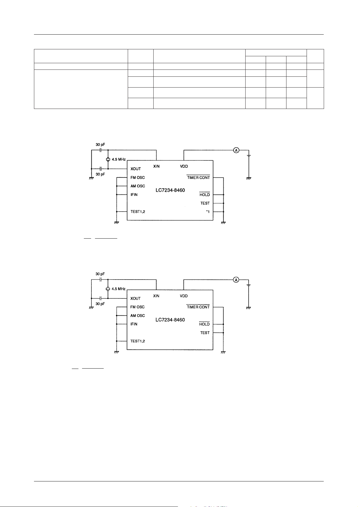
Measurement Circuits
Hold mode I
DD2
LC7234-8460
sgnitaR
nimpytxam
M
I
I
I
I
V
1DD
2DD
3DD
4DD
1DD
V
2DD
V
DD
V
DD
V,2MOC,1MOC
f,
2NI
I,V5=
DD
zHM031=5102
tiucrictnemerusaem
Aµ02=0.25.20.3V
O
edomdloH,gnitarepoLLP,
52=aT,gnitareporotallicsO,V5.5=°,C
tiucrictnemerusaemedompukcaB
52=aT,deppotsrotallicsO,V2.2=°,C
tiucrictnemerusaemedompukcaB
7.0
tinU
Am
5
Aµ
1
Note
*1 = pins K0 to K3, SD, STEREO, BAND0 and BAND1
Pins T0 to T8, TIMER OUT, FM, AMUTE, SW, M/S(L), FM/AM, MO/ST = open
Backup mode I
DD3
Note
Pins K0 to K4, SD, STEREO, BAND0, B AND1, T0 to T8, TIMER OUT, FM, AMUTE, SW, M/S(L), FM/AM, MO/ST,
S1 to S23, COM1, COM2 = open
No.4350–4/23
Page 5
Functional Description
Band Coverage
noigeRdnaB
MF0.801ot0.7805/001527.01
aWM2061ot13599864/054
anihC
1setatSdetinU
2setatSdetinU
eporuE
tsaEelddiM
1nommoC
2nommoC
ailartsuA,adanaC
dlroW
bWM1161ot22599864/054
1WS32.6ot82.255054
2WS58.12ot1.755054
MF9.701ot5.78002057.01
bWM0171ot0350101054
MF0.801ot5.78001057.01
bWM0171ot0350101054
MF0.801ot5.7805/001527.01
aWM2061ot13599864/054
bWM1161ot22599864/054
WL182ot64111864/054
MF0.801ot5.7805/001527.01
aWM2061ot13599864/054
bWM1161ot22599864/054
1WS32.6ot82.255054
2WS58.12ot1.755054
MF0.801ot5.7805/001527.01
aWM2061ot13599864/054
bWM2061ot13599864/054
AWS6.51ot59.555054
MF0.801ot5.7805/001527.01
aWM2061ot13599864/054
bWM1161ot22599864/054
BWS5.21ot8.355054
MF0.801ot5.7805/001527.01
bWM1161ot22599864/054
MF0.801ot5.7805/001527.01
aWM2061ot13599864/054
bWM1161ot22599864/054
WL182ot64111864/054
BWS5.21ot8.355054
LC7234-8460
egnarycneuqerF
])zHk(MA)zHM(WS,MF[
petsycneuqerF
)zHk(
nosirapmoC
)zHk(ycneuqerf
ycneuqerfretneC
2B1B0B
])zHk(MA)zHM(MF[
000
001aWM2061ot13599864/054
010aWM2061ot13599864/054
100
011
101
110
111aWM2061ot13599864/054
1=DLROW
Band Selection
When SELBND is 0, BAND0 and BAND1 select the
frequency band as shown in the following table. When
1DNAB0DNAB
00 MFMFMFMFMFMF
01 )MF(WL1WS)MF()MF(WL
10 MAWMWMWMWMWM
11 )MF()MF(2WSAWSBWSBWS
,adanaC,.A.S.U
ailartsuA
eporuE
SELBND is 1, the BAND, FM, MW, LW and SW keys
select the frequency band.
,tsaEelddiM
anihC
1nommoC2nommoCdlroW
The frequency band selection determines the logic levels
of FM/AM, M/S(L), SW and FM as shown in the following table.
DNAB
MFHGIHWOLWOLWOL
WMWOLHGIHWOLHGIH
)WL(1WSWOLWOLWOLHGIH
2WSWOLWOLHGIHHGIH
MA/MF)L(S/MWSMF
emanniP
Preset Memory Channels
seulavyromemteserPsdnabycneuqerfforebmuN
2HCSP1HCSPMFWMWL/1WS2WS
008888
015555
10 61 888
11 lagellI
No.4350–5/23
Page 6
LC7234-8460
SW band search ranges Key/diode Matrix
DNAB)zHM(egnarycneuqerF
1WS
2WS
AWS
BWS
594.2ot82.2
4.3ot2.3
0.4ot8.3
60.5ot57.4
32.6ot59.5
3.7ot1.7
9.9ot5.9
5.21ot56.11
8.31ot6.31
6.51ot1.51
9.71ot55.71
58.12ot54.12
32.6ot59.5
3.7ot1.7
9.9ot5.9
5.21ot56.11
8.31ot6.31
6.51ot1.51
0.4ot8.3
60.5ot57.4
32.6ot59.5
3.7ot1.7
9.9ot5.9
5.21ot56.11
Diode matrix functions
edoiD
xirtam
eman
KCOLC
H42/21
NOLOC
TNCFI
FILES
MFLES
WMLES
RMTLES
DLROW
0snoitcnufkcolctuohtiW
1snoitcnufkcolchtiW
0kcolcruoh-21
1kcolcruoh-42
0sm005rofFFO,sm005rofNO.gnihsalF
1NO
0oN
1seY
0zHk054
1zHk864
0zHk001
1zHk05
0tcelesegnarycneuqerfaWM
1tcelesegnarycneuqerfbWM
0remittuohtiW
1remithtiW
0tcelesdnabtupnilevel-cigoL
DNABLES
1tcelesdnabhctiwsyratnemoM
02Bdna1B,0BgnisutcelesdnaB
1dnabDLROWstceleS
FFO/NOnoitcnuF
Function positions
tuptuO
0TNOREMIT/1HCFFOREMIT/2HC3HC4HC
1T5HC6HC7HC8HC
2TPUNWODSPEM
3TDNABTS/OMPEELSYALPSID
4TMFWM)1WS(WL
5T0B1B2B
6TKCOLCH42/21NOLOCTNCFI
7TFILESMFLESWMLESRMTLES
8TDNBLES1HCSP2HCSPDLROW
0K1K2K3K
tupnI
Notes
1. A indicates that the diode matrix element has either of the following configuations.
2. No indicates that the diode matrix element has a momentary switch configuation.
)2WS(,WS
)BWS(,)AWS(
No.4350–6/23
Page 7
LC7234-8460
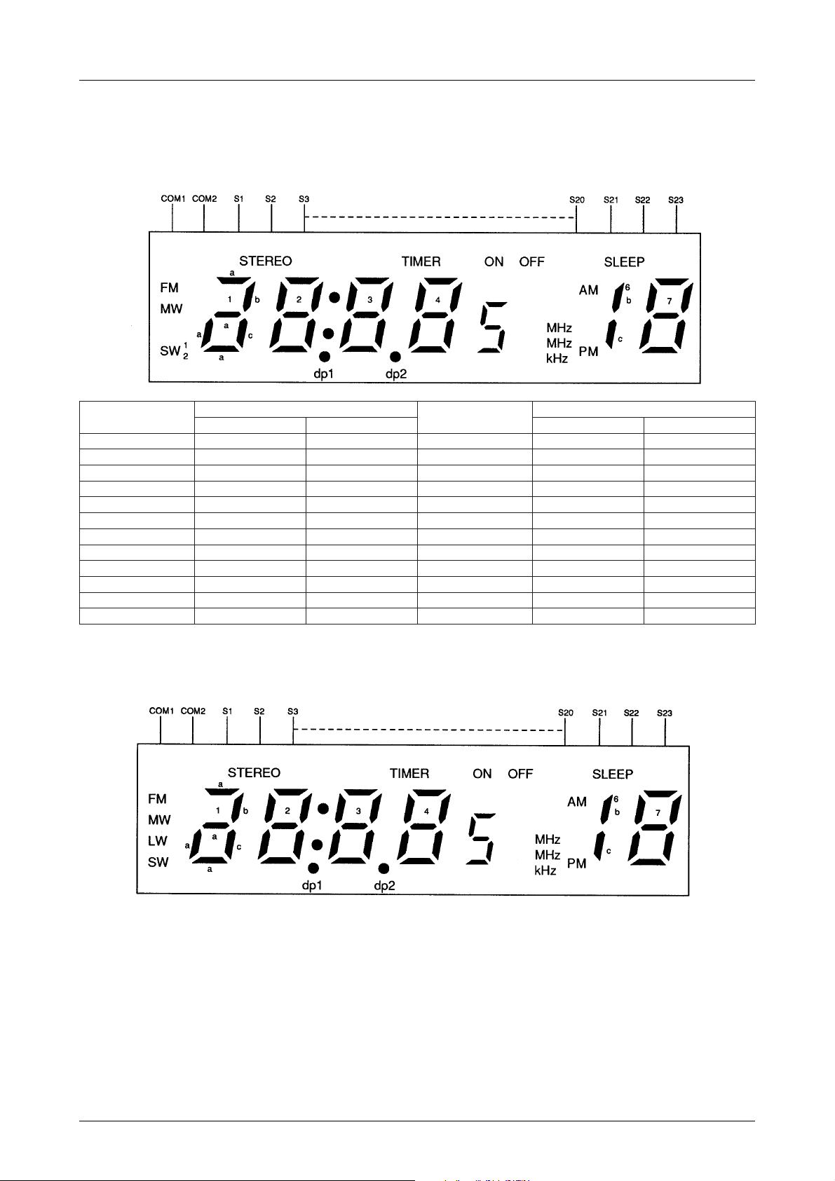
LCD Display Driver
China and the Middel East
The configuation of the LCD panel used in China and the
Middle East only is shown in the following figure, and
the pin-to-segment relationship, in the following table.
tuptuotnemgeS
1S1 zHk·WM31Sf4a4
2SzHM·1pd·WSzHM·2pd·MF41Sb4g4
3Sa12 51Se4c4
4Sc1b161Sd4REMIT
5Sf2a271SNOFFO
6Sb2g281S5MA
7Se2c291Sf7a7
8Sd2OERETS02Sb7g7
9Sf3a312Se7c7
01Sb3g322Sd7PEELS
11Se3c332Sc,b6MP
21Sd3NOLOC
1MOC2MOC1MOC2MOC
tuptuorevirdnommoC
All other regions
The configuration of the LCD panel used in all regions
other than China and the Middle East is shown in the
tuptuotnemgeS
tuptuorevirdnommoC
following figure, and the pin-to-segment relationship, in
the following table.
No.4350–7/23
Page 8

LC7234-8460
tuptuotnemgeS
1SzHkWM31Sf4a4
2SzHM·1pd·1WSzHM·2pd·MF41Sb4g4
3Sa1WL51Se4c4
4Sc1b161Sd4REMIT
5Sf2a271SNOFFO
6Sb2g281S5MA
7Se2c291Sf7a7
8Sd2OERETS02Sb7g7
9Sf3a312Se7c7
01Sb3g322Sd7PEELS
11Se3c332Sc,b6MP
21Sd3NOLOC
1MOC2MOC1MOC2MOC
tuptuorevirdnommoC
Hold Mode
When the clock is enabled and HOLD makes a HIGH-toLOW transition, the FMOSC, AMOSC, IFIN and TEST
inputs are disabled and only the clock operates. In this
mode, the supply current is reduced to 0.7 mA (typ).
Backup Mode
When the clock is disabled and HOLD makes a HIGHto-LOW transition, the FMOSC, AMOSC, IFIN and
TEST inputs are disabled and the 4.5MHz crystal
oscillator is halted. In this mode, the supply current is
reduced to 5 µA (max).
As AMUTE becomes high impedance in backup mode, a
pull-down resistor should be connected between AMUTE
and ground.
Key Functions
Frequency display
PSCH2 and PSCH1 = LOW
Write mode
When ME is pressed, the flashing preset number ‘P’
appears and the system enters write mode for 5 seconds.
If one of the preset memory keys CH1 to CH8 is pressed
within 5 seconds, the presently selected frequency and
status are written to the corresponding channel.
If ME is pressed while ‘P’ is displayed, write mode is
extended.
When the same preset memory key is pressed twice,
AMUTE goes HIGH.
If any other key is pressed or if HOLD makes a HIGHto-LOW transition, write mode is canceled.
Read mode
When one of the preset memory keys CH1 to CH8 is
pressed, the corresponding frequency and status are
displayed.
PSCH2 = LOW and PSCH1 = HIGH
Write mode
When ME is pressed, the flashing preset number ‘P’
appears and the system enters write mode for 5 seconds.
If one of the preset memory keys CH1 to CH5 is pressed
within 5 seconds, the presently selected frequency and
status are written to the corresponding channel.
tuptuotnemgeS
tuptuorevirdnommoC
If ME is pressed while ‘P’ is displayed, write mode is
extended. When the same preset memory key is pressed
twice, AMUTE goes HIGH.
If any other key is pressed or if HOLD makes a HIGHto-LOW transition, write mode is canceled.
Read mode
When one of the preset memory keys CH1 to CH5 is
pressed, the corresponding frequency and status are
displayed.
PSCH2 = HIGH and PSCH1 = LOW
Write mode
When ME is pressed, a flashing ‘P1’ appears in the
frequency display area and the system enters write mode
for 5 seconds.
If one of the preset memory keys CH1 to CH8 is pressed
within 5 seconds, the frequency and status are written to
the corresponding channel of channels 1 to 8.
When the FM band is selected, pressing ME while ‘P1’ is
flashing changes the display to a flashing ‘P2’. If one of
the preset memory keys CH1 to CH8 is then pressed
within 5 seconds, the frequency and status are written to
the corresponding channel of channels 9 to 16.
If ME is pressed while ‘P2’ is flashing, write mode is
canceled.
When the AM band is selected, pressing ME while ‘P1’ is
flashing cancels the write mode.
Read mode
When the FM band is selected and one of the preset
memory keys CH1 to CH8 is pressed once, the frequency
and status are read from the corresponding channel of
channels 1 to 8.
If one of the preset memory keys is pressed twice, the
frequency and status are read from the corresponding
channel of channels 9 to 16.
When the AM band is selected and one of the preset
memory keys CH1 to CH8 is pressed, the corresponding
frequency is read out.
No.4350–8/23
Page 9

LC7234-8460
UP and DOWN
When HOLD is HIGH, each time UP or DOWN is
pressed, the frequency will go up or down by one step,
respectively. If you hold down one of these keys for more
than 500 ms, autosearch mode will start, and the next
broadcasting station in the corresponding direction will
be searched for. The search speed is 60 ms/step for the
FM band and 70 ms/step for the AM band.
Autosearch pauses for 500 ms when either key is pressed,
regardless of whether a station has been detected, and
then resumes. Autosearch searches from one edge of the
band to the other, pauses for 500 ms and then resumes
searching.
BAND
When HOLD is HIGH, BAND is used to select the
frequency band. Each time BAND is pressed, the frequency band will change as shown in figures 1 and 2.
The band select keys are shown in figure 3.
Figure 1. Band selection (WORLD = 0)
separating colon start flashing and the system enters set
mode. In this mode, use UP to alter the minute and
DOWN to after the hour. The segments continue flashing
between UP and DOWN key operations.
UP
Each time UP is pressed, the minute setting increases by
1. If UP is held down for more than 500 ms, the minute
setting increases at a rate of 8 min/s.
When adjusting the minute setting, the second setting is
reset to 0 s. The second setting cannot be adjusted
independently from the minute setting.
DOWN
Each time DOWN is pressed, the hour setting increases
by 1. If DOWN is held down for more than 500 ms, the
hour setting increases at a rate of 4 hr/s.
The second setting is not changed when adjusting the
hour setting.
Canceling set mode
If no key is pressed for 5 s or ME is pressed twice, set
mode is canceled automatically.
If any other key is pressed, set mode is canceled and the
key operation is executed.
Figure 2. Band selection (WORLD = 1)
Figure 3. Band select keys
PS
When PS is pressed, the channel number changes to the
next highest channel number than the one currently
selected. If no channel number is currently selected, then
channel number 1 is selected. In this case, AMUTE will
go LOW for 5 s if a signal is received.
During PS mode, the channel number flashes at 1 Hz
(500 ms ON and 500 ms OFF).
PS mode is canceled if any of PS, UP, DOWN, CH1 to
CH8, or BAND are pressed, or if HOLD makes a HIGH-
to-LOW transition.
MO/ST
MO/ST is used when receiving in the FM band. When
MO/ST is pressed, the MO/ST port output will toggle
between mono and stereo.
Clock display
When the clock or timer setting is displayed, CH3 to
CH8 function in the same way as when the frequency is
displayed.
When ME is pressed, the hour and minute digits and the
Timer display
When CH1/TIMER ON is pressed, the ON time is
selected, ‘TIMER’ and ‘ON’ are displayed, the hour and
minute digits and the separating colon start flashing (500
ms ON and 500 ms OFF), and the system enters set
mode. In this mode, use UP to alter the minute and
DOWN to alter the hour.
When CH2/TIMER OFF is pressed, the OFF time is
selected, ‘TIMER’ and ‘OFF’ are displayed, the hour and
minute digits and the separating colon start flashing (500
ms ON and 500 ms OFF), and the system enters set
mode. In this mode, use UP to alter the minute and
DOWN to alter the hour.
Figure 4. Timer setting
The timer setting mode is canceled by pressing the same
key twice or by pressing a mode cancel input key. If no
key is pressed, the timer setting mode is canceled automatically after five seconds.
UP
Each time UP is pressed, the minute setting increases by
1. If UP is held down for more than 500 ms, the minute
setting increases at a rate of 8 min/s.
No.4350–9/23
Page 10

LC7234-8460
DOWN
Each time DOWN is pressed, the hour setting increases
by 1. If DOWN is held down for more than 500 ms, the
hour setting increases at a rate of 4 hr/s.
Other keys
DISPLAY
When HOLD is HIGH and the clock is enabled (DIMRX
CLOCK =1), use DISPLAY to change what is displayed.
Each time DISPLAY is pressed, the display toggles
SLEEP
SLEEP is used to set the sleep time. If SLEEP is pressed
while ‘SLEEP’ is not displayed, ‘SLEEP’ and ‘90’ appear
on the display. Each time SLEEP is pressed while the
sleep time is displayed, the sleep time decreases by 10
minutes. Five seconds after setting the sleep time, the
previous display is restored. If the sleep time is set to 0,
the ‘SLEEP’ display disappears and the sleep mode
setting is canceled.
If the sleep time has already been set, SLEEP can be
pressed to check the remaining sleep time even while the
frequency or clock is displayed. After 5 s, the previous
display is restored.
UP or DOWN
When you press either key, the hour and minute digits
and the separating colon stop flashing and remain ON.
between the frequency display and clock displays as
shown in the following figure.
When in sleep mode, TIMER OUT is HIGH.
TEST
When TEST is pressed and HOLD makes a LOW-to-
HIGH transition, all segments of the LCD turn ON. If
TEST is pressed again, the clock display turns ON,
assuming there is a clock, and starts counting at a rate of
1 min/s. If there is no clock, pressing TEST a second
time cancels the test.
Tracking Point Frequency
noigeRdnaB
anihC
1setatSdetinU
2setatSdetinU
eporuE
tsaEelddiM
lennahC
1HC2HC3HC4HC8HCot5HClennahctsaL
MF0.781.091.891.6010.780.78
aWM1353069994041135135
bWM2253069994041225225
1WS82.2594.20.40.682.282.2
2WS1.75.91.5154.121.71.7
MF5.781.091.891.6015.785.78
aWM1353069994041135135
bWM03500600010041035035
MF5.781.091.891.6015.785.78
aWM1353069994041135135
bWM03500600010041035035
MF5.780.090.890.6015.785.78
aWM1353069994041135135
bWM2253069994041225225
WL641461902362641641
MF5.780.090.890.6015.785.78
aWM1353069994041135135
bWM2253069994041225225
1WS82.2594.20.40.682.282.2
2WS1.75.91.5154.121.71.7
Continued on next page.
No.4350–10/23
Page 11

LC7234-8460
Continued from preceding page.
noigeRdnaB
MF5.780.090.890.6015.785.78
1nommoC
2nommoC
ailartsuA,adanaC
dlroW
aWM1353069994041135135
bWM2253069994041225225
AWS59.52.69.98.3159.559.5
MF5.780.090.890.6015.785.78
aWM1353069994041135135
bWM2253069994041225225
BWS8.300.51.756.118.38.3
MF5.780.090.890.6015.785.78
aWM1353069994041135135
bWM2253069994041225225
MF5.780.090.890.6015.785.78
aWM1353069994041135135
bWM2253069994041225225
WL641461902362641641
BWS8.300.51.756.118.38.3
Power-up Status
If momentary switches are connected to the band select
inputs, the lower edge of the FM band is selected on
power-up. If rocker switches are connected, the band is
determined by the input states of BAND1 and BAND0.
1HC2HC3HC4HC8HCot5HClennahctsaL
lennahC
On power-up, the MO/ST status is set to mono, the
display indicates the tuning frequency, the clock is set to
12:00 and the timer is set to 10:00.
Timing Diagrams
Automatic Up/down Scanning
Table 1. IF count tolerance
MF zHk01±zHM7.01
WM zHk3±864/054
WS zHk5.1±054
WL zHk6.0±864/054
Notes
1. When using an IF count, SD is checked twice at 5 ms intervals. If both checks are successful, SD is recognized.
2. When not using an IF count, SD is checked three times at 5 ms intervals. If all three checks are successful, SD is
recognized.
Scanning with UP and DOWN
No.4350–11/23
Page 12

Timer Functions
Timer example 1
Notes
1. Timer ON time is 10:00.
2. Timer OFF time is 12:00.
Timer example 2
LC7234-8460
Note
Timer ON and OFF times are both 10:00.
Simultaneous sleep and timer operation
If the following figures, the timer ON time is 10:00 and the
timer OFF time is 12:00.
No.4350–12/23
Page 13

LC7234-8460
Audio Mute
The timing periods shown in the following diagram represent the following times.
1. Key debounce reject time (40 ms)
2. Audio mute lead time and EDO output delay (50 ms)
BAND and CH1 to CH8 initiated muting
UP and DOWN initiated muting
Note
If a band edge is encountered during period 4, the length of period 4 changes to 500 to 625 ms.
3. PLL data and display processing time (30 to 50 ms)
4. Audio mute trailing time
No.4350–13/23
Page 14

PS initiated muting
Auto up/down function initiated muting
Hold Mode
LC7234-8460
Backup Mode
Note
A pull-down resistor should be connected to AMUTE.
No.4350–14/23
Page 15

LC7234-8460
T ypical Applications
Without Clock (Clock = 0), Momentary Switch Band Select
No.4350–15/23
Page 16

LC7234-8460
With Clock (Clock = 1), Momentary Switch Band Select
No.4350–16/23
Page 17

LC7234-8460
With Clock (Clock = 1), Logic-level Input Band Select
No.4350–17/23
Page 18

LC7234-8460
Without Clock (Clock = 0), Momentary Switch Band Select
No.4350–18/23
Page 19

LC7234-8460
With Clock (Clock = 1), Momentary Switch Band Select
No.4350–19/23
Page 20

LC7234-8460
With Clock (Clock = 1), Logic-level Input Band Select
No.4350–20/23
Page 21

2-band AM/FM Electronic Tuning Radio
LC7234-8460
No.4350–21/23
Page 22

Peripheral Components Interface
LC7234-8460
No.4350–22/23
Page 23

LC7234-8460
Specifications of any and all SANYO products described or contained herein stipulate the performance,
characteristics, and functions of the described products in the independent state, and are not guarantees
of the performance, characteristics, and functions of the described products as mounted in the customer's
products or equipment. To verify symptoms and states that cannot be evaluated in an independent device,
the customer should always evaluate and test devices mounted in the customer's products or equipment.
SANYO Electric Co., Ltd. strives to supply high-quality high-reliability products. However, any and all
semiconductor products fail with some probability. It is possible that these probabilistic failures could
give rise to accidents or events that could endanger human lives, that could give rise to smoke or fire,
or that could cause damage to other property. When designing equipment, adopt safety measures so
that these kinds of accidents or events cannot occur. Such measures include but are not limited to protective
circuits and error prevention circuits for safe design, redundant design, and structural design.
In the event that any or all SANYO products(including technical data,services) described or
contained herein are controlled under any of applicable local export control laws and regulations,
such products must not be exported without obtaining the export license from the authorities
concerned in accordance with the above law.
No part of this publication may be reproduced or transmitted in any form or by any means, electronic or
mechanical, including photocopying and recording, or any information storage or retrieval system,
or otherwise, without the prior written permission of SANYO Electric Co. , Ltd.
Any and all information described or contained herein are subject to change without notice due to
product/technology improvement, etc. When designing equipment, refer to the "Delivery Specification"
for the SANYO product that you intend to use.
Information (including circuit diagrams and circuit parameters) herein is for example only ; it is not
guaranteed for volume production. SANYO believes information herein is accurate and reliable, but
no guarantees are made or implied regarding its use or any infringements of intellectual property rights
or other rights of third parties.
This catalog provides information as of October, 2001. Specifications and information herein are subject
to change without notice.
PS No.4350–23/23
 Loading...