

Page 1
Any and all SANYO products described or contained herein do not have specifications that can handle
applications that require extremely high levels of reliability, such as life-support systems, aircraft’s
control systems, or other applications whose failure can be reasonably expected to result in serious
physical and/or material damage. Consult with your SANYO representative nearest you before using
any SANYO products described or contained herein in such applications.
SANYO assumes no responsibility for equipment failures that result from using products at values that
exceed, even momentarily, rated values (such as maximum ratings, operating condition ranges,or other
parameters) listed in products specifications of any and all SANYO products described or contained
herein.
CMOS IC
Single-Chip PLL and Microcontroller
with LCD Driver
Ordering number:ENN*4117
LC7233N
SANYO Electric Co.,Ltd. Semiconductor Company
TOKYO OFFICE Tokyo Bldg., 1-10, 1 Chome, Ueno, Taito-ku, TOKYO, 110-8534 JAPAN
Preliminary
Overview
The LC7233N is a single-chip microcontroller that incorporates a 0.5 to 150 MHz phase-locked loop (PLL) and a
liquid-crystal display (LCD) driver , making it ideal for digital tuners. It has a large number of input/output ports and a
frequency measurement circuit.
The LC7233N features on-chip RAM and ROM, a programmable high-speed divider, a 6-bit analog-to-digital con v erter
and a low-voltage detection reset circuit.
The LC7233N operates from a 5 V supply and is available
in 64-pin QIPs.
Features
• 0.5 to 150 MHz phase-locked loop.
• LCD driver.
• 6-bit analog-to-digital converter.
• Two 8-bit PWM digital-to-analog converters.
• Two 4-bit input ports.
• Two 4-bit input/output ports.
• 6-bit keypad matrix scan output port.
• 2-bit open-drain high-voltage output port.
• 23 mask-selectable output drivers.
• 20-bit universal counter.
• 4096 × 16-bit program ROM (001H to FFFH user addres-
sable memory).
• 256 × 4-bit data RAM.
• Low-voltage detection reset circuit.
• Programmable high-speed divider.
• Single-word instructions.
• Four-level stack.
• PLL-unlocked flip-flop.
• Timer flip-flop.
• External interrupt.
• Programmable watchdog interrupt address.
• Standby mode.
• CPU operates down to 3.5 V and retains data down to
1.3 V.
• 5 V supply.
• 64-pin QIP.
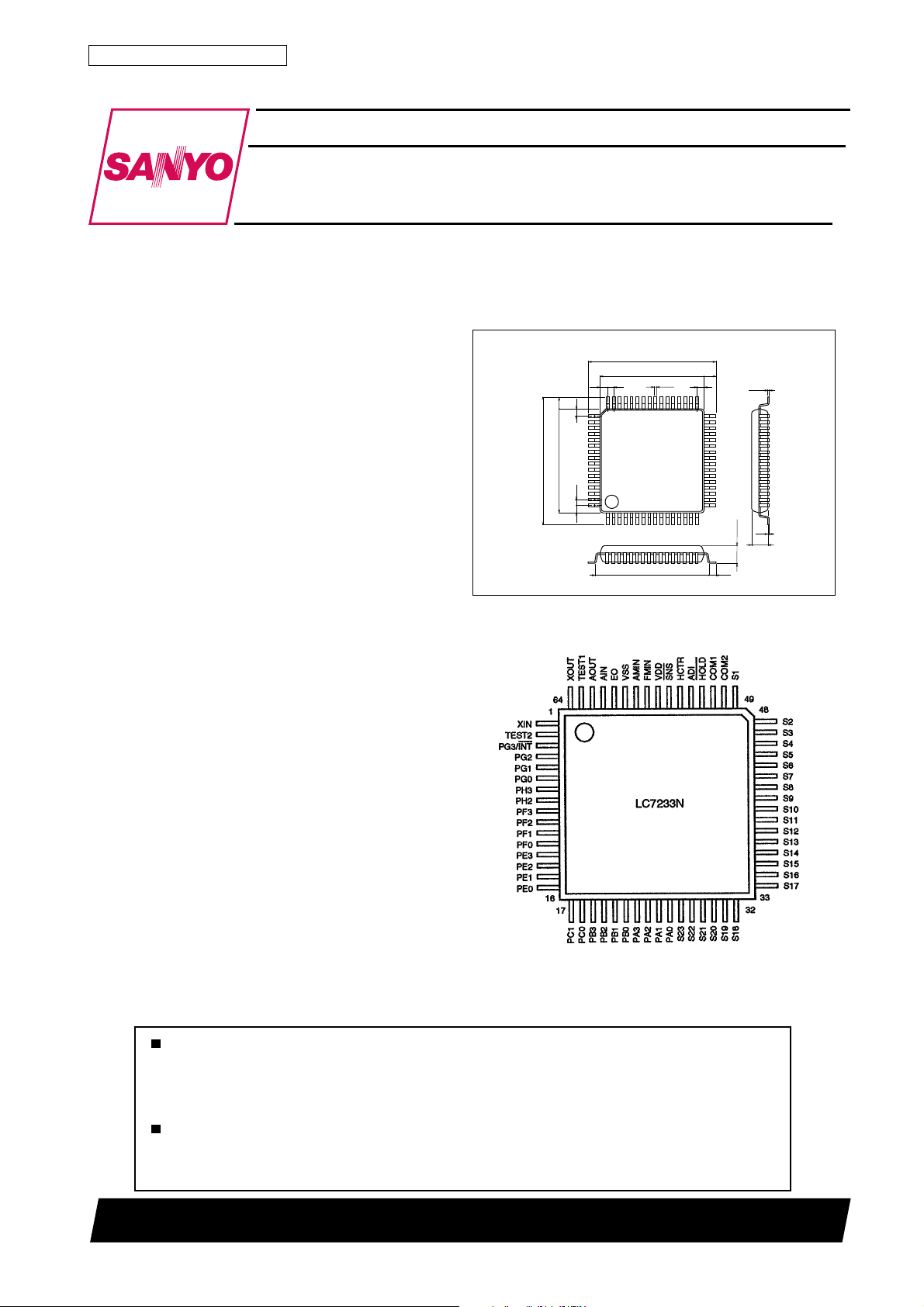
Package Dimensions
unit:mm
3159-QIP64E
[LC7233N]
17.2
14.0
0.8
0.35
15.6
17.2
1.6
14.0
1.0
48
1.0
49
0.8
64
1.0
1
Pin Assignment
Top view
1.6
1.0
33
32
17
16
0.8
SANYO : QIP64E
3.0max
0.15
0.1
2.7
80101TN (KT)/3062JIN No.4117–1/12
Page 2
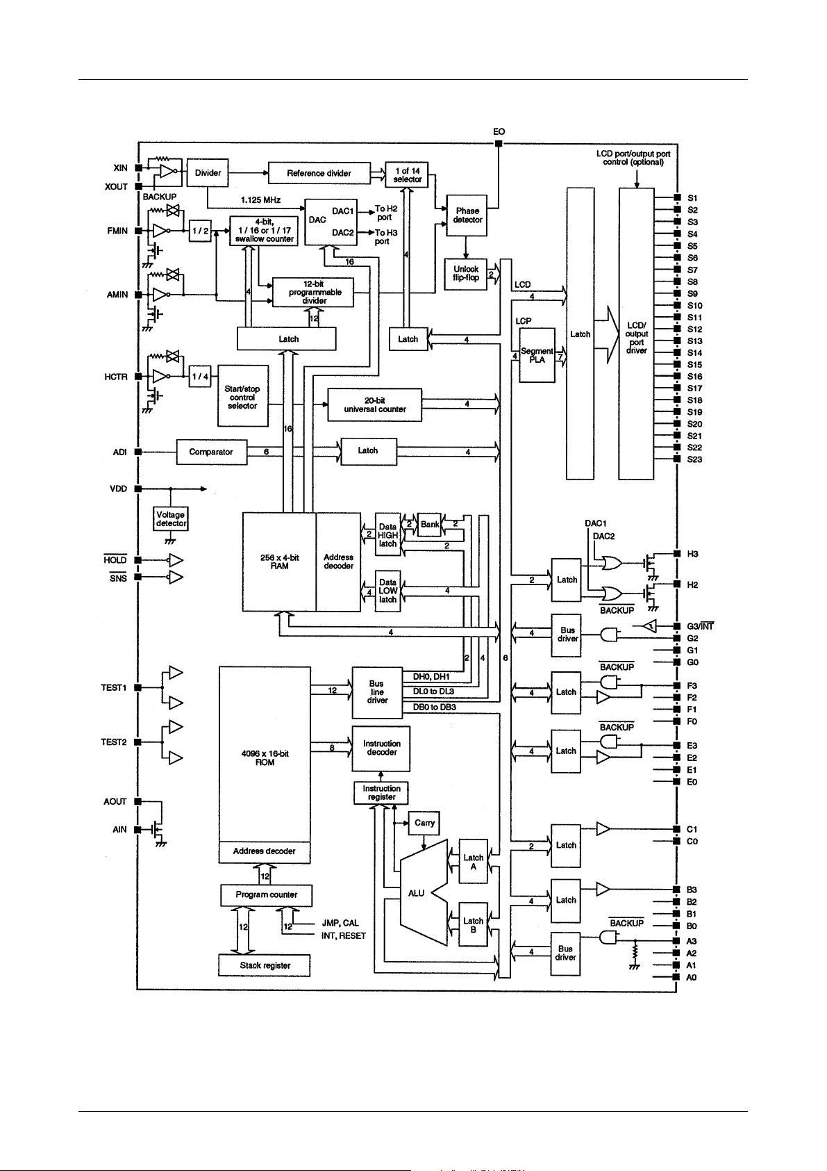
Block Diagram
LC7233N
No.4117–2/12
Page 3
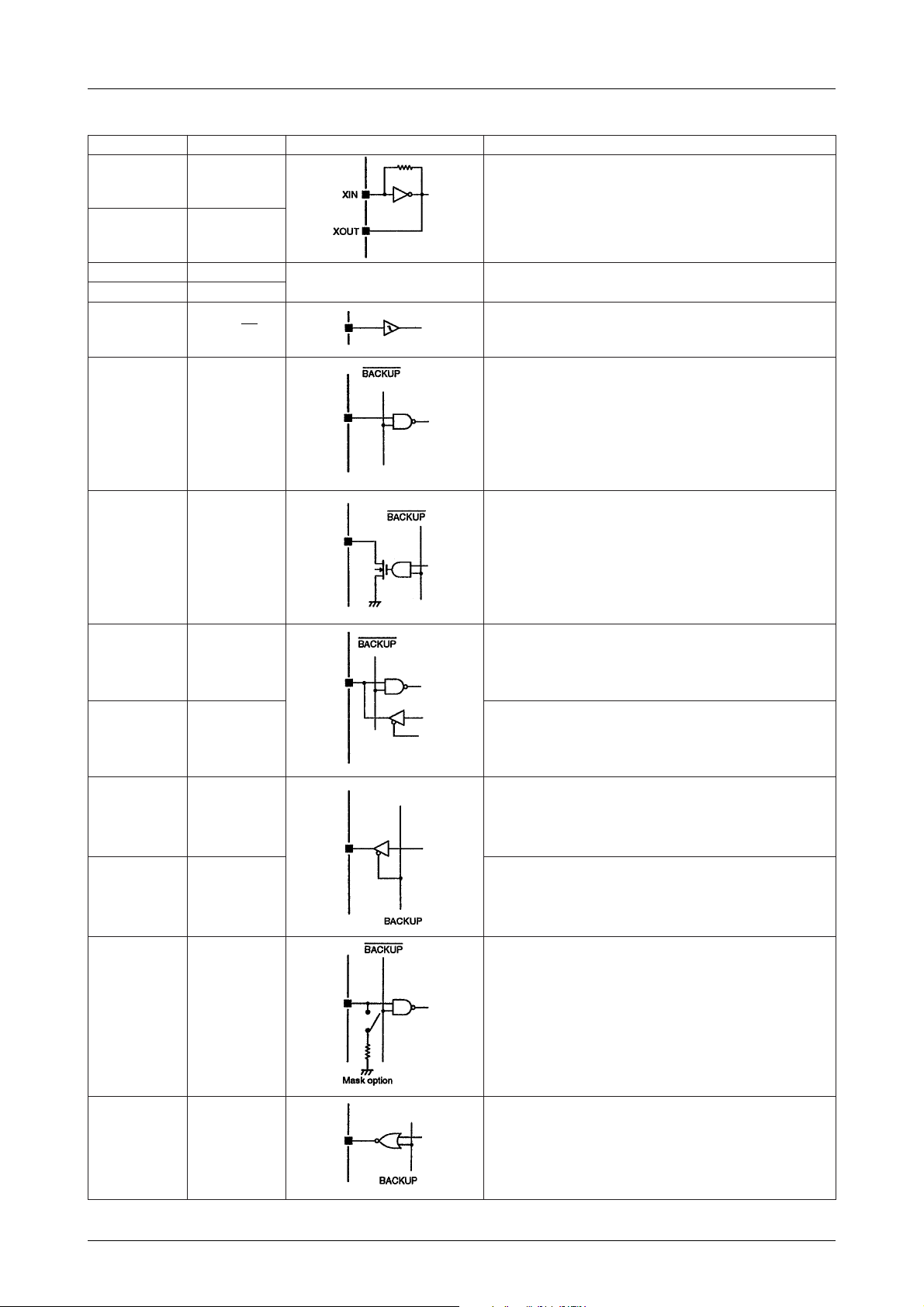
Pin Description
rebmuNemaNtiucrictnelaviuqEnoitpircseD
1NIX
46TUOX
LC7233N
snoitcennocrotallicsolatsyrC
22TSET
361TSET
3TNI/3GP tupnitseuqertpurretnidnatibGtroptupnidexelpitluM
6ot40GPot2GPGtroptupnI
8,70HP,1HPHtroptuptuO
21ot90FPot3FP Ftroptuptuo/tupnI
sniptseT
61ot310EPot3EP Etroptuptuo/tupnI
81,710CP,1CPCtroptuptuO
22ot910BPot3BPBtroptuptuO
62ot320APot3APAtroptupnI
94ot721Sot32S stuptuotnemgesDCL
Continued on next page.
No.4117–3/12
Page 4
Continued from preceding page.
rebmuNemaNtiucrictnelaviuqEnoitpircseD
15,051MOC,2MOC stuptuorevirdnommocDCL
25DLOH tupnilortnocedom-dloH
55SNStcetedliaf-rewoP
35IDAtupniretrevnocD/A
LC7233N
45RTCH tupniretnuoclasravinU
65V
75NIMFtupniOCVMF
85NIMAtupniOCVMA
95V
06OE tuptuorotarapmocesahP
16NIAtupnigolanA
DD
SS
ylppusV5
dnuorG
26TUOAtuptuogolanA
No.4117–4/12
Page 5

LC7233N
Specifications
Absolute Maximum Ratings
retemaraPlobmySsnoitidnoCsgnitaRtinU
egatlovylppuSV
egatlovtupniSNSdnaIDA,DLOH,GtroPV
)stupnirehto(egatlovtupnIV
egatlovtuptuoTUOAdnaHtroPV
)stuptuorehtolla(egatlovtuptuOV
tnerructuptuoHtroPI
tnerructuptuoFdnaEstroPI
tnerructuptuoCdnaBstroPI
tnerructuptuoTUOAI
noitapissidrewopelbawollAxamdP 004Wm
erutarepmetgnitarepOrpoT –58+ot04
erutarepmetegarotSgtsT –521+ot54
Recommended Operating Conditions at Ta = 25˚C
retemaraPlobmySsnoitidnoCsgnitaRtinU
egatlovylppuSV
)UPCdnaLLP(egnaregatlovylppuSV
)UPC(egnaregatlovylppuSV
noitneteratadrofegnaregatlovylppuSV
DD
1I
2I
1O
2O
1O
2O
3O
4O
DD
1DD
2DD
3DD
–5.6+ot3.0V
–0.31+ot3.0V
–Vot3.0
–0.51+ot3.0V
–Vot3.0
3.0+
DD
DD
V
3.0+
V
5ot0
Am
3ot0
Am
1ot0
Am
2ot0
Am
˚C
˚C
5V
5.5ot5.4V
5.5ot5.3V
5.5ot3.1V
Electrical Characteristics at Ta = –40 to +85˚C, VDD = 3.5 to 5.5V, unless otherwise noted
retemaraPlobmySsnoitidnoC
tnerrucylppuSI
tnerrucylppusedom-dloHI
tnerrucylppusedom-ybdnatSI
egatlovtupnilevel-wolTNI/3GPdnaAtroPV
egatlovtupnilevel-wolFdnaEstroPV
egatlovtupnilevel-wol2GPot0GPV
egatlovtupnilevel-wolDLOHV
egatlovtupnilevel-wolSNSV
egatlovtupnilevel-hgihAtroPV
egatlovtupnilevel-hgihFdnaEstroPV
egatlovtupnilevel-hgih2GPot0GPV
egatlovtupnilevel-hgihTNI/3GPdnaDLOHV
egatlovtupnilevel-hgihSNSV
edutilpmatupnismrNIXV
edutilpmatupnismrNIMFV
edutilpmatupnismrNIMAV
edutilpmatupnismrRTCHV
htdiwsiseretsyhtupniTNI/3GPV
egatlovtupniIDAV
egatlovtupniAtroPV
egatlovdlohserhtybdnatSV
ycneuqerftupniNIXf
ycneuqerftupniNIMFf
)egnarwol(ycneuqerftupniNIMAf
)egnarhgih(ycneuqerftupniNIMAf
ycneuqerftupniRTCHf
htdiwesluptcejerSNSP
tnerructupnilevel-wolFdnaE,AstroPI
tnerructupnilevel-wolNIAI
tnerructupnilevel-wolRTCHdnaNIMA,NIMFI
f
1DD
I
2DD
VDD=5.5V, oscillator halted, Ta=25˚C
3DD
V
DD
1LI
2LI
3LI
4LI
5LI
1HI
2HI
3HI
4HI
5HI
1I
2I
3I
4I
SYH
5I
FI
TED
VI=V5.1ot5.00.45.40.5zHM
1I
VI=,V5.1ot1.0V
2I
VI=,V5.1ot51.0V
VI=,V5.1ot1.0V
3I
VI=,V5.1ot1.0V
4I
VI=,V5.1ot1.0V
5I
jer
1LI
VIV=
2LI
VIV=
3LI
V,zHM031=
DD
t,detlahLLP
cyc
cyc
t,detlahLLP
cyc
=2.5V, oscillator halted, Ta=25˚C
Ron
DPV.IV=SS
SS
SS
V5.5ot5.4=5102Am
V,sµ76.2=
DD
V,sµ33.31=
DD
V,sµ00.04=
DD
=V5.5ot5.401031
DD
=V5.5ot5.401051
DD
=V5.5ot5.45.00.01zHM
DD
=V5.5ot5.4204zHM
DD
=V5.5ot5.44.00.21zHM
DD
RsahAtroP.ecnadepmihgihsiAtroP
V5.5ot5.3=5.1
V5.5ot5.3=0.1
V5.5ot5.3=7.0
.
DP
nimpytxam
V6.0
V7.0
V7.0
V8.0
V1.0
sahAtroP.ecnadepmihgiheraFdnaEstroP
sgnitaR
0V2.0
0V3.0
0V3.0
0V4.0
03.1V
DD
DD
DD
DD
7.20.8V
5.05.1V
1.05.1V
1.05.1V
1.05.1V
DD
0V
7.20.33.3V
40103Aµ
V
V
V50.0
10.00.01An
tinU
Amt,detlahLLP
5
Aµ
1
V
DD
V
DD
V
DD
V
DD
V
DD
V
DD
0.8V
0.8V
V
V
DD
V
DD
zHM
05sµ
3Aµ
Continued on next page.
No.4117–5/12
Page 6

Continued from preceding page.
retemaraPlobmySsnoitidnoC
tnerruc
tnerructupnilevel-wolNIXI
tnerructupnilevel-hgihAtroPI
tnerructupnilevel-hgihNIAI
tnerruc
tnerructupnilevel-hgihNIXI
egatlovtuptuolevel-wolHtroPV
egatlovtuptuolevel-wolTUOAV
egatlovtuptuolevel-wolOEV
egatlovtuptuolevel-wolTUOXV
egatlovtuptuolevel-hgihOEV
tnerruc
tnerruc
rorreretrevnocD/A
ecnatsisernwod-llupAtroPR
LC7233N
tupnilevel-wolGtropdnaSNS,IDA,DLOH
tnerructupnilevel-hgihFdnaE,AstroPI
tupnilevel-hgihGtropdnaSNS,IDA,DLOH
egatlovtuptuolevel-wolCdnaBstroPV
egatlovtuptuolevel-wolFdnaEstroPV
egatlovtuptuolevel-wol2MOCdna1MOCV
egatlovtuptuolevel-wol32Sot1SV
egatlovtuptuolevel-dim2MOCdna1MOCV
egatlovtuptuolevel-hgihCdnaBstroPV
egatlovtuptuolevel-hgihFdnaEstroPV
egatlovtuptuolevel-hgih2MOCdna1MOCV
egatlovtuptuolevel-hgih32Sot1SV
egatlovtuptuolevel-hgihTUOXV
egakaeltuptuolevel-wolFdnaE,C,BstroP
tnerrucegakaeltuptuolevel-wolOEI
egakaeltuptuolevel-hgihFdnaE,C,BstroP
tnerrucegakaeltuptuolevel-hgihHtroPI
tnerrucegakaeltuptuolevel-hgihTUOAI
tnerrucegakaeltuptuolevel-hgihOEI
I
VIV=
4LI
5LI
1HI
2HI
tnerructupnilevel-hgihRTCHdnaNIMA,NIMFI
3HI
4HI
I
5HI
6HI
1LO
2LO
3LO
4LO
5LO
6LO
7LO
8LO
1M
1HO
2HO
3HO
4HO
5HO
6HO
I
1LFFO
2LFFO
I
1HFFO
2HFFO
3HFFO
4HFFO
ε
DP
SS
VIV=
SS
Ron
DPV.IV=DD
VIV=
DD
VIV=
DD
VIV=
VIV5.5= 3Aµ
VIV=
I
O
I
O
I
O
I
O
I
O
I
O
I
O
I
O
V
IO1=Am
IO=Am1
I
O
I
O
IO=– Am1.0
I
O
VOV=
VOV=
VOV=
VOV31= 5Aµ
VOV31= 1Aµ
VOV=
V
VDDV5=57001002kΩ
V0.5=40103Aµ
DD
V0.5= 2551Aµ
DD
Aµ05=5.00.10.2V
Am1= 1V
Am5=
V,Am5=
NIA
Aµ52=3.05.057.0V
Aµ005= 1V
Am1.0= 1V
Aµ002= 1V
I,V5=
DD
O
Aµ52=
Aµ005=
Aµ002=
SS
SS
DD
DD
DD
V5.5ot5.4=–2/12/1bsl
RsahAtroP,V0.5=
.05Aµ
DP
V3.1=5.0V
Aµ02=0.25.20.3V
sgnitaR
nimpytxam
2551Aµ
sahAtroP.ecnadepmihgiheraFdnaEstroP
57.0
051( Ω)
VDD–0.2VDD–0.1VDD–5.0
VDD–0.1
VDD–57.0
VDD–0.1
VDD–0.1
VDD–0.1
VDD–5.0VDD–3.0
3Aµ
3Aµ
10.00.01An
0.2
004( Ω)
3Aµ
10.00.01Aµ
3Aµ
10.00.01An
tinU
V
V
V
V
V
V
V
Test Circuits
Hold mode
Notes
1. Ports E and F are selected as output ports.
2. Ports A to H, S1 to S23, COM1 and COM2 are open.
No.4117–6/12
Page 7

LC7233N
Standby mode
Note
Ports A to H, S1 to S23, COM1 and COM2 are open.
Functional Description
LCD Driver
The LC7233N can drive LCD segments. The LCP and
LCD instructions transfer data to the LCD outputs. The
LCD instruction transfers data directly to the LCD
outputs. The LCP instruction converts data to 7-segment
format before transfer to the outputs.
S1 to S23 are the driver outputs. The LCD frame rate is
100 Hz with a 50% duty cycle. After reset or power-up, a
blank signal is present on all outputs. In standby mode,
all outputs are LOW. They can be used as generalpurpose outputs if the appropriate mask option is selected.
COM1 and COM2 are the LCD common driver outputs.
Output drive is 50% duty with 50% bias. Upon reset or
after power-up, the normal drive signals are present on
these outputs. In standby mode, all outputs are LOW.
Frequency Counter
Frequency measurement is performed at the HCTR input
by the 20-bit universal counter. The input frequency
range is 0.4 to 12 MHz, which is used for measuring AM
and FM IF frequencies. Capacitive coupling should be
used.
Input/Output Ports
Port A
This input port has a low switching threshold, which is
used for keypad matrix inputs. Pull-down resistors for all
pins are available as a mask option. Note that either all or
none of the pins should have pull-down resistors. In
standby mode, inputs are ignored.
Ports B and C
These output ports have unbalanced CMOS outputs
which are used as keypad matrix scan outputs. Upon
reset, outputs are set LOW, and in standby mode, outputs
are high impedance. The outputs can be short-circuited.
Port E
The transfer direction of this input/output port is selected
automatically under software control. When an input
instruction (IN, TPT, or TPF) is executed, port E is
configured for input operation, and an output instruction
(OUT, SPB or RPB), for output operation. Upon reset, all
pins become inputs. In standby mode, the output drivers
are high impedance and the input signals are ignored. All
bits should either be inputs or outputs.
Phase-locked Loop
The FMIN or AMIN input signal is divided down by a
programmable divider, and then compared with the
crystal frequency, which is also divided down using 14
selectable ratios. The phase difference between the two
signals is measured using a phase detector and output on
EO.
FMIN is the input pin for the FM VCO input signal. The
input frequency range is 10 to 130 MHz. Capacitive
coupling should be used.
AMIN is the AM VCO input. The bandwidth is adjustable in two ranges by using the PLL instruction-HIGH (2
to 40 MHz) for the SW band, and LOW (0.5 to 10 MHz),
for the LW and MW bands. Capacitive coupling should
be used.
Port F
The transfer direction of this input/output port is selected
by the FPC instruction. Each pin of this port can be set
independently to be an input or output. Upon reset, all
pins become inputs. In standby mode, the output drivers
are high impedance and the input signals are ignored.
Port G
PG0 to PG2 are inputs only. PG3/INT can be used as a
standard input or as the interrupt request input. In
standby mode, inputs are ignored.
No.4117–7/12
Page 8

LC7233N
Port H
These output ports are high-voltage, n-channel opendrain drivers, which are used for switching power
supplies. Upon reset and in standby mode, outputs are
high impedance. Port H can also be configured as the
output of DAC1 and DAC2.
A/D Converter
The A/D converter is a 6-bit successive approximation
type. The conversion cycle time is 1.28 ms. Full-scale
output data is 3FH for an input of (63/96) × VDD.
Power-fail Detection
When connected to the supply, SNS is used as a powerfail detector. SNS can also be used as a standard input
port.
Crystal Oscillator
The master crystal oscillator, which has a feedback
resistor on-chip, requires only the connection of a 4.5
MHz crystal.
Low-power Modes
Hold mode
When the hold-mode control pin, HOLD, is driven LOW
and the HOLDEN (hold enable) flip-flop has previously
been set by an SS instruction, the LC7233N enters hold
mode.
HOLD has a high-voltage input (VIH(max) = 8.0 V)
which can be connected directly to the power supply.
Standby mode
When the LC7233N is in hold mode and HOLD is LOW,
standby mode can be set by the CKSTP instruction.
Test Pins
Two device test pins are provided-TEST1 and TEST2.
These should either be tied to VSS or left open.
Instruction Set
ADDR Program memory address [12 bits]
b Borrow
B Bank number [2 bits]
C Carry
DH Data memory address high-order bits (row address) [2 bits]
DL Data memory address low-order bits (column address) [4 bits]
I Immediate data [4 bits]
M Data memory address
N Bit position [4 bits]
Pn Port number [4 bits]
r General register (Bank 0 addresses 00H to 0FH)
Rn Register number [4 bits]
( ) Contents of register or memory
( )n Contents of bit N of register or memory
No.4117–8/12
Page 9

LC7233N
cinomenM
dnarepO
noitarepO
tamrofnoitcurtsnI
noitatoNnoitpircseD
pikS
noitidnoc
ts1dn2
51D41D31D21D11D01D9D8D7D6D5D4D3D2D1D0D
ddA
DArM
.rotMddA
010000 HDLDnRr← )M(+)r(
ehtserotsdnarfostnetnocehtotMfostnetnocehtsddA
.rnitluser
SDArM
fipiksdnarotMddA
.yrrac
010001 HDLDnR
r ← ,)M(+)r(
yrracfipiks
ehtserotsdnarfostnetnocehtotMfostnetnocehtsddA
.detarenegsiyrracafispikS.rnitluser
yrraC
CArM
.yrrachtiwrotMddA
010010 HDLDnRr← C+)M(+)r(
dnaCdnarfostnetnocehtotMfostnetnocehtsddA
.rnitluserehtserots
SCArM
yrrachtiwrotMddA
.yrracfipiksdna
010011 HDLDnR
r ← ,C+)M(+)r(
yrracfipiks
dnaCdnarfostnetnocehtotMfostnetnocehtsddA
.detarenegsiyrracafispikS.rnitluserehtserots
yrraC
IAMI
.MotIddA
010100 HDLDIM← I+)M(
serotsdnaMfostnetnocehtotatadetaidemmiehtsddA
.Mnitlusereht
SIAMI
fipiksdnaMotIddA
.yrrac
010101 HDLDI
M ← ,I+)M(
yrracfipiks
serotsdnaMfostnetnocehtotatadetaidemmiehtsddA
.detarenegsiyrracafispikS.Mnitlusereht
yrraC
CIAMI
.yrrachtiwMotIddA
010110 HDLDIM← C+I+)M(
dnaCdnaMfostnetnocehtotatadetaidemmiehtsddA
.Mnitluserehtserots
SCIAMI
yrrachtiwMotIddA
.yrracfipiksdna
010111 HDLDI
M ← ,C+I+)M(
yrracfipiks
dnaCdnaMfostnetnocehtotatadetaidemmiehtsddA
.detarenegsiyrracafispikS.Mnitluserehtserots
yrraC
tcartbuS
USrM
.rmorfMtcartbuS
011000 HDLDnR
r ← ,)M(–)r(
yrracfipiks
dnarfostnetnocehtmorfMfostnetnocehtstcartbuS
.rnitluserehtserots
SUSrM
dnarmorfMtcartbuS
.worrobfipiks
011001 HDLDnR
r ← ,)M(–)r(
worrobfipiks
dnarfostnetnocehtmorfMfostnetnocehtstcartbuS
.detarenegsiworrobafispikS.rnitluserehtserots
worroB
BSrM
htiwrmorfMtcartbuS
.worrob
011010 HDLDnRr← b–)M(–)r(
htiwrfostnetnocehtmorfMfostnetnocehtstcartbuS
.rnitluserehtserotsdnaworrob
SBSrM
htiwrmorfMtcartbuS
fipiksdnaworrob
.worrob
011011 HDLDnR
r ← ,b–)M(–)r(
worrobfipiks
htiwrfostnetnocehtmorfMfostnetnocehtstcartbuS
siworrobafispikS.rnitluserehtserotsdnaworrob
.detareneg
worroB
ISMI
.MmorfItcartbuS
011100 HDLDIM← I–)M(
dnaMfostnetnocehtmorfatadetaidemmiehtstcartbuS
.Mnitluserehtserots
SISMI
dnaMmorfItcartbuS
.worrobfipiks
011101 HDLDI
M ← ,I–)M(
worrobfipiks
dnaMfostnetnocehtmorfatadetaidemmiehtstcartbuS
.detarenegsiworrobafispikS.Mnitluserehtserots
worroB
BISMI
htiwMmorfItcartbuS
.worrob
011110 HDLDIM← b–I–)M(
htiwMfostnetnocehtmorfatadetaidemmiehtstcartbuS
.Mnitluserehtserotsdnaworrob
SBISMI
htiwMmorfItcartbuS
fipiksdnaworrob
.worrob
011111 HDLDI
M ← ,b–I–)M(
worrobfipiks
htiwMfostnetnocehtmorfatadetaidemmiehtstcartbuS
siworrobafispikS.Mnitluserehtserotsdnaworrob
.detareneg
worroB
erapmoC
QESrM
.MslauqerfipikS
000001 HDLDnRorezfipiks,)M(–)r(
erayehtfispiksdnaMdnarfostnetnocehtserapmoC
.lauqe
)M(=)r(
EGSrM
nahtretaergsirfipikS
.Motlauqero
000011 HDLDnR
,)M(–)r(
)r(fipiks ≥ )M(
retaergsirfispiksdnaMdnarfostnetnocehtserapmoC
.Motlauqeronaht
)M()r(
IQESMI
.IslauqeMfipikS
001101 HDLDI orezfipiks,I–)M(
dnaMfostnetnocehtotatadetaidemmiehtserapmoC
.lauqeerayehtfispiks
0=I–)M(
IEGSMI
retaergsiMfipikS
.Iotlauqeronaht
001111 HDLDI
,I–)M(
)M(fipiks ≥ I
dnaatadetaidemmiehthtiwMfostnetnocehtserapmoC
.IotlauqeronahtretaergsiMfispiks
I)M(
Continued on next page.
No.4117–9/12
Page 10
LC7233N
cinomenM
dnarepO
noitarepO
tamrofnoitcurtsnI
noitatoNnoitpircseD
pikS
noitidnoc
ts1dn2
51D41D31D21D11D01D9D8D7D6D5D4D3D2D1D0D
citemhtiracigoL
DNAMI
.MhtiwIDNA
001100 HDLDIM← )M(I
ehtdnaatadetaidemmiehtfoDNA-cigolehtsetaluclaC
.MnitluserehtserotsdnaMfostnetnoc
ROMI
.MhtiwIRO
001110 HDLDIM← I)M(
ehtdnaatadetaidemmiehtfoRO-cigolehtsetaluclaC
.MnitluserehtserotsdnaMfostnetnoc
LXErM
.rhtiwMRO-evisulcxE
001000 HDLDnRr← )r( ⊕ )M(
dna,MdnarfostnetnocehtfoROX-cigolehtsetaluclaC
.rnitluserehtserots
erotsdnadaoL
DLrM
.rotniMdaoL
100000 HDLDnRr← )M(
.rotMfostnetnocehtsevoM
TSMr
.MnirerotS
100001 HDLDnRM← )r(
.MotrfostnetnocehtsevoM
DRVMrM
MotMevoM
.nRybdesserdda
100010 HDLDnR]nR,HD[ ← )M(
HDybdecnerefersserddaehtotMfostnetnocehtsevoM
.nRdna
SRVMMr
ybdesserddaMevoM
.MotnR
100011 HDLDnRM← ]nR,HD[
ybdecnerefernoitacolyromemehtfostnetnocehtsevoM
.MotnRdnaHD
RSVMM
1
M
2
.MotMevoM
100100 HDLD
1
LD
2
LD.HD[
1
] ← LD.HD[
2
]
yromemot2noitacolyromemehtfostnetnocehtsevoM
.1noitacol
IVMMI
.MotIevoM
100101 HDLDIM← I
.MotatadetaidemmiehtsevoM
LLPMr
LLPotMdaoL
.sretsiger
100110 HDLDnRrLLP ← )M(
.sretsigerLLPehtotMfostnetnocehtsevoM
tsettiB
TMTMN
piksdnaMfostibtseT
eurtfi
101001 HDLDN 1lla=)N(Mfipiks
fispikS.NybdeificepsMnoitacolyromemfostibehtstseT
.1cigolerastiblla
stibllA
1=deificeps
FMTMN
piksdnaMfostibtseT
eslaffi
101011 HDLDN 0lla=)N(Mfipiks
fispikS.NybdeificepsMnoitacolyromemfostibehtstseT
.0cigolerastiblla
stibllA
0=deificeps
enituorbusdnapmuJ
PMJRDDA
sserddaotpmuJ
1011 )stib21(RDDACP ← RDDA
.RDDAybdeificepssserddaehtotspmuJ
LACRDDA
enituorbusllaC
1100 )stib21(RDDA
kcatS ← ,1+)CP(
CP ← RDDA
.RDDAybdeificepsenituorbusehtotspmuJ
TR
enituorbusmorfnruteR
1101010000000000CP ← kcats
.enituorbusamorfsnruteR
ITR
tpurretnimorfnruteR
1101010100000000CP ← kcats
.tpurretniamorfsnruteR
tsetgalF
MTTN
polf-pilfremittseT
110101100000 N 0=F/FremitfipikS
.orezfispiksdnapolf-pilfremitehtstseT 0=F/FremiT
LUTN
polf-pilfLLPtseT
110101110000 N 0=F/FLLPfipikS
.orezfispiksdnapolf-pilfdekcolnu-LLPehtstseT0=F/FLLP
tesdnatsetretsigersutatS
SSN
stibretsigersutatsteS
110111000000 N
N)1retsigersutatS( ← 1
.Nybdeificeps1retsigersutatsfostibehtsteS
SRN
retsigersutatsteseR
stib
110111010000 N
N)1retsigersutatS( ← 0
.Nybdeificeps1retsigersutatsfostibehtsteseR
TSTN
retsigersutatstseT
eurtfipiksdnastib
110111100000 N
)2retsigersutats(fipikS
1lla=N
llafispikS.Nybdeificeps2retsigersutatsfostibehtstseT
.1erastib
stibllA
1=deificeps
FSTN
retsigersutatstseT
eslaffipiksdnastib
110111110000 N
)2retsigersutats(fipikS
0lla=N
llafispikS.Nybdeificeps2retsigersutatsfostibehtstseT
.0erastib
stibllA
0=deificeps
tcelesknaB
KNABB
knabtceleS
110100 B 00000000
KNAB ← B
.sknabyromemruoffoenostceleS
Continued on next page.
Continued from preceding page.
No.4117–10/12
Page 11

LC7233N
cinomenM
dnarepO
noitarepO
tamrofnoitcurtsnI
noitatoNnoitpircseD
pikS
noitidnoc
ts1dn2
51D41D31D21D11D01D9D8D7D6D5D4D3D2D1D0D
tuptuo/tupnI
DCLMI
DCLotatadevoM
.stnemges
111000 HDLDTIGID
)TIGID(DCL ← M.revirdDCLehtotyltceridatadetaidemmiehtsdaoL
PCLMI
atadtnemges-7evoM
.DCLot
111001 HDLDTIGID
)TIGID(DCL ← ALP ←
M
agnisutamroftnemges-7otatadetaidemmiehtstrevnoC
.revirdDCLehtottisrefsnartnehtALP
NIMnP
.MotatadtropevoM
111010 HDLDP
M ← ))P(trop(.MotnPtroptupnimorfatadehtsevoM
TUOMnP
.tropotatadevoM
111011 HDLDP
))P(trop( ← M.nPtropotMnoitacolyromemfostnetnocehtsevoM
BPSnPN
.stibtropteS
11110000 P N
N))P(trop( ← 1.1cigolotNybdeificepsnPtropfostibehtsteS
BPRnPN
.stibtropteseR
11110101 P N
N))P(trop( ← 0.0cigolotNybdeificepsnPtropfostibehtsteS
TPTnPN
dnatropfostibtseT
.eurtfipiks
11111010 P N
1lla=N))P(trop(fipikS
erastibllafispikS.NybdeificepsnPtropfostibehtstseT
.1cigol
stibllA
1=deificeps
FPTnPN
dnatropfostibtseT
.eslaffipiks
11111111 P N
0lla=N))P(trop(fipikS
erastibllafispikS.NybdeificepsnPtropfostibehtstseT
.0cigol
stibllA
0=deificeps
retnuoclasrevinU
SCUI
.1WCCUteS
000000010000 I
1WCCU ← I.1galfretnuoclasrevinuehtsteS
CCUI
.2WCCUteS
000000110000 I
2WCCU ← I.2galfretnuoclasrevinuehtsteS
suoenallecsiM
CPFN
.lortnocnoitceridFtroP
000100000000 N
hctalCPF ← N
nitibafI.FtropfosniplaudividnifonoitceridehtsenifeD
eht,CPFybtessiretsigernoitceridFtropeht
.tuptuonasemocebFtropfonipgnidnopserroc
PTSKC
.kcolcpotS
0001000100000000
0=DLOHfikcolcpotS0=DLOHfikcolcrossecorpehtspotS
PON
noitarepooN
000000000000
noitarepooN
Continued from preceding page.
No.4117–11/12
Page 12
LC7233N
Mask Option
retemaraPsnoitpO
)TDW(remitgodhctaW
eht(Atropnosrotsisernwod-lluP
)troptupnixirtamdapyek
emitelcycnoitcurtsnIsµ76.2
Development System
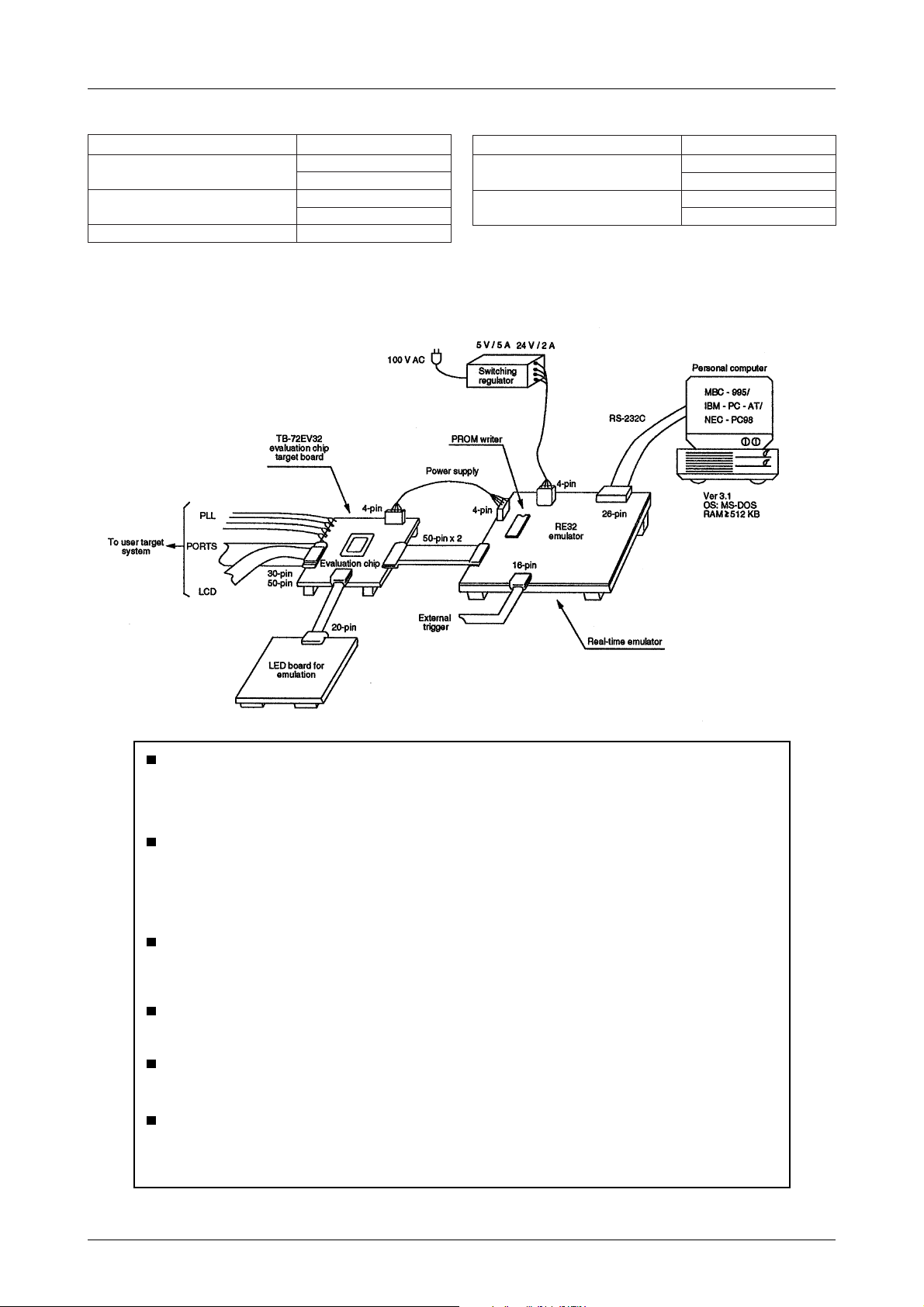
The LC7223N development environment is shown in the
following figure. It uses an LC72EV32 evaluation chip
mounted on a TB-72EV32 target board and a multifunc-
seY
oN
seY
oN
retemaraPsnoitpO
emitelcycnoitcurtsnI
noitarugifnoc32Sot1S
sµ33.31
sµ00.04
troptuptuorevirdDCL
troptuptuoesoprup-lareneG
tional emulator (RE32), which is controlled by a personal
computer, to provide full debugging facilities.
Specifications of any and all SANYO products described or contained herein stipulate the performance,
characteristics, and functions of the described products in the independent state, and are not guarantees
of the performance, characteristics, and functions of the described products as mounted in the customer's
products or equipment. To verify symptoms and states that cannot be evaluated in an independent device,
the customer should always evaluate and test devices mounted in the customer's products or equipment.
SANYO Electric Co., Ltd. strives to supply high-quality high-reliability products. However, any and all
semiconductor products fail with some probability. It is possible that these probabilistic failures could
give rise to accidents or events that could endanger human lives, that could give rise to smoke or fire,
or that could cause damage to other property. When designing equipment, adopt safety measures so
that these kinds of accidents or events cannot occur. Such measures include but are not limited to protective
circuits and error prevention circuits for safe design, redundant design, and structural design.
In the event that any or all SANYO products(including technical data,services) described or
contained herein are controlled under any of applicable local export control laws and regulations,
such products must not be exported without obtaining the export license from the authorities
concerned in accordance with the above law.
No part of this publication may be reproduced or transmitted in any form or by any means, electronic or
mechanical, including photocopying and recording, or any information storage or retrieval system,
or otherwise, without the prior written permission of SANYO Electric Co. , Ltd.
Any and all information described or contained herein are subject to change without notice due to
product/technology improvement, etc. When designing equipment, refer to the "Delivery Specification"
for the SANYO product that you intend to use.
Information (including circuit diagrams and circuit parameters) herein is for example only ; it is not
guaranteed for volume production. SANYO believes information herein is accurate and reliable, but
no guarantees are made or implied regarding its use or any infringements of intellectual property rights
or other rights of third parties.
This catalog provides information as of August, 2001. Specifications and information herein are subject to
change without notice.
PS No.4117–12/12
 Loading...