

Page 1

Ordering number : ENN∗7143
CMOS IC
LC72311W, 72312W, 72313W
Low-Voltage ETR-Controller
Preliminary
Overview
The LC72311W, LC72312W, and LC72313W are
low-voltage single-chip FM/AM electronic tuning
microcontrollers that include a built-in PLL circuit for
frequencies up to 230 MHz, a 1/4 duty 1/2 bias LCD
controller, and a small EEPROM. These microcontroller
also provide a low-power standby mode that reduces power
consumption by switching the system clock frequency.
Furthermore, since these devices include a low-pass filter
amplifier required for the electronic tuning system and a
tuning voltage generator circuit, they can contribute to
reduced end product costs through lower parts counts.
These ICs are optimal for use in low-voltage portable audio
equipment that includes a radio receiver.
Functions
•
Program memory (ROM):
8192 × 16 bits (16 KB) LC72311W
16,384 × 16 bits (32 KB) LC72312W
24,576 × 16 bits (48 KB) LC72313W
•
Data memory (RAM):
512 × 4 bits (RAM)
512 × 4 bits (EEPROM)
•
Cycle time:
0.71 µs (at 4.2336 MHz) (All 1-word instructions)
40 µs (at 75 kHz) (All 1-word instructions)
•
Stack: 8 levels
•
LCD driver:
48 to 96 segments (1/4 duty 1/2 bias drive)
•
Interrupts:
Two external interrupt systems
Internal timer interrupts: two systems (1, 5, 10, and 50 ms)
Serial I/O interrupt (SIO0 only)
■ Any and all SANYO products described or contained herein do not have specifications that can handle
applications that require extremely high levels of reliability, such as life-support systems, aircraft’s control
systems, or other applications whose failure can be reasonably expected to result in serious physical and/or
material damage. Consult with your SANYO representative nearest you before using any SANYO products
described or contained herein in such applications.
■ SANYO assumes no responsibility for equipment failures that result from using products at values that exceed,
even momentarily, rated values (such as maximum ratings, operating condition ranges, or other parameters)
listed in products specifications of any and all SANYO products described or contained herein.
•
A/D converter:
Four-input 8-bit converter
•
Input ports:
9 or 10 ports (Ports PA, PF, and HCTR)
The PF port is shared with the A/D converter, and HCTR
is shared with the IF counter.
•
Output ports:
8 ports (Ports PB and PE)
PE3 is shared with the BEEP pin, PE0 to PE2 are
open-drain ports, and the PB port can be switched to
function as an open-drain port.
Continued on next page.
Package Dimensions
unit: mm
3220-SQFP80
[LC72311W, 72312W , 72313W]
14.0
12.0
1.25 1.25
0.5
0.2
0.5
14.0
60
61
1.25
0.5
12.0
1.25
80
120
0.135
41
40
21
1.4
1.6max
0.1
0.5
SANYO: SQFP80
N3001RM(OT)No.7143-1/9
Page 2

LC72311W, 72312W, 72313W
Continued from preceding page.
•
I/O ports:
22 ports (Ports PC, PD, PL, PI, PG, and PH)
Port PD is shared with the interrupt function, ports PC and
PK are shared with th e ser ial I /O funct ion, and p ort s PI, P G,
and PH are shared with the LCD segment driver function.
•
PLL:
Provides dead band control (4 settings)
Reference frequencies: 1, 3, 3.125, 5, 6.25, 12.5, and 25
kHz
•
Input frequencies:
FM band: 10 to 230 MHz
AM band: 0.5 to 10 MHz
•
Input sensitivity:
FM band: 35 mVrms (130 MHz to 50 mVrms)
AM band: 35 mVrms
•
HCTR:
IF counter (0.4 to 15 MHz)
•
External reset pin:
Starts the PC from address 0 during CPU and PLL
operation.
•
Built-in power-on reset circuit:
Starts the PC from address 0 at power on.
•
Halt mode:
Temporarily slows the microcontroller operating clock
and reduces power consumption.
•
Backup mode:
Stops the crystal oscillator circuit.
•
Static power on:
Backup mode can be cleared with the PF port.
•
BEEP:
Seven alarm tones: 0.75, 1.25, 1.5, 2.08, 2.5, 3.125, and
6.25 kHz.
•
Serial I/O:
Two channels (These functions use the PC and PK port
pins.)
The internal serial transfer clock provides three
frequencies: 12.5, 25, and 75 kHz.
•
On-chip low-pass filter amplifier:
Reduces end product parts counts and costs.
•
Tuning voltage generator circuit:
Obviates the need for an external tuning power supply
circuit for reduced end product parts counts and costs.
•
Memory retention voltage:
Over 0.9 V.
•
VDD voltage:
PLL circuit: 1.8 to 3.6 V
CPU and A/D converter:
1.6 to 3.6 V (For a 40 µs instruction cycle)
2.4 to 3.6 V (For a 0.71 µs instruction cycle)
•
Option selections:
PH0 to PH3/S13 to S16
PG0 to PG3/S17 to S20
PI0 to PI3/S21 to S24
Vsense circuit present/absent
•
Package:
SQFP80 (0.5 mm lead pitch)
No.7143-2/9
Page 3
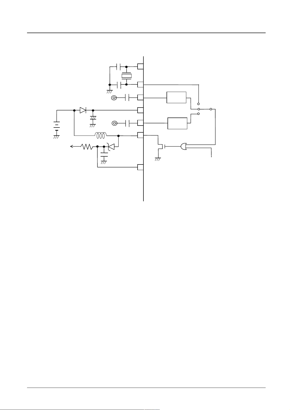
Tuning Voltage Generator Circuit
LC72311W, 72312W, 72313W
XIN
80
XOUT
1
1/256
1/2
FM
AM
PLL instruction
100 µH
72
VDD
71
AMIN
73
TU
67
14 V
VDDP
68
No.7143-3/9
Page 4

Specifications
LC72311W, 72312W, 72313W
Absolute Maximum Ratings at Ta = 25°°°°C, V
= 0 V
SS
Parameter Symbol Conditions Ratings Unit
V
max −0.3 to +4.0 V
Maximum supply voltage
Input voltage V
Output voltage
Output current
DD
VDDPmax −0.3 to +16.0 V
All input pins −0.3 to V
IN
V
1 AOUT, PE0 to 2, TU −0.3 to +15 V
OUT
2 All output pins other than V
V
OUT
I
1 PC, PD, PE3, PG, PH, PI, PK, PL, EO 0 to 3 mA
OUT
I
2 PB 0 to 1 mA
OUT
I
3 AOUT, PE0 to 2, TU 0 to 2 mA
OUT
I
4 S1 to S24 300 µA
OUT
5 COM1 to COM4 3 mA
I
OUT
1 −0.3 to V
OUT
+ 0.3 V
DD
+ 0.3 V
DD
Allowable power dissipation Pdmax Ta = −20 to +70°C 300 mW
Operating temperature Topr −20 to +70 °C
Storage temperature Tstg −45 to +125 °C
Allowable Operating Ranges at Ta = −−−−20 to ++++70°°°°C, V
Parameter Symbol Conditions
VDD1 PLL operating voltage 1.8 3.0 3.6
VDD2 Memory retention voltage 1.0
Supply voltage
High-level input voltage
Low-level input voltage
Input amplitude
Input voltage range VIN6 ADI0, ADI1, ADI2, ADI3 0 VDD V
Input frequency
VDD3 CPU operating voltage 1.6 3.0 3.6
VDD4 A/D converter operating voltage 1.6 3.0 3.6
VDDP1 Voltage applied to the VDDP pin 13 14 15
VIH1
Input ports other than V
and DIN (with amplifier circuit)
IH
VIH2 BRES 0.8 VDD V
3 The PF port 0.6 VDD V
V
IH
VIL1
Input ports other than V
and DIN (with amplifier circuit)
IL
VIL2 BRES 0 0.2 VDD V
3 The PF port 0 0.2 VDD V
V
IL
VIN1 XIN 0.5 0.6 Vrms
VIN2 FMIN,AMIN 0.035 0.35 Vrms
VIN3 FMIN 0.05 0.35 Vrms
V
4 HCTR and DIN (with amplifier circuit) 0.035 0.35 Vrms
IN
F
1 XIN CI ≤ 35 kΩ 70 75 80 kHz
IN
FIN2 FMIN: VIN2, VDD1 10 130 MHz
FIN3 FMIN: VIN3, VDD1 130 230 MHz
FIN4 AMIN (H): VIN2, VDD1 2 40 MHz
FIN5 AMIN (L): VIN2, VDD1 0.5 10 MHz
FIN6 HCTR: VIN4, VDD1 0.4 12 MHz
FIN7 DIN (with amplifier circuit): VIN4, VDD1 2 18 MHz
F
8 DIN (without amplifier circuit): VIH1, VDD1 2 18 MHz
IN
==== 1.8 to 3.6 V
DD
2, VIH3, AMIN, FMIN, HCTR, XIN,
2, VIL3, AMIN, FMIN, HCTR, XIN,
Ratings
min typ max
0.7 V
V
DD
0 0.3 V
Unit
V
V
DD
V
DD
V
DD
V
DD
No.7143-4/9
Page 5

LC72311W, 72312W, 72313W
Electrical Characteristics in the Allowable Operating Ranges
Parameter Symbol Conditions
High-level input current
Low-level input current
I
1 XIN: VI = VDD = 3.0 V 3 µA
IH
FMIN, AMIN, HCTR, DIN (with amplifier circuit):
IIH2
VI = V
= 3.0 V
DD
The PA/PF (without pull-down resistors), PC, PD, PG, PH,
3
PI, PK, and PL ports, BRES, and DIN (without amplifier
I
IH
circuit): VI = V
I
1 XIN: VI = VDD = VSS −3 µA
IL
IIL12
FMIN, AMIN, HCTR, DIN (with amplifier circuit):
VI = V
DD
= V
SS
= 3.0 V
DD
The PA/PF (without pull-down resistors), PC, PD, PG, PH,
13
I
PI, PK, and PL ports, BRES, and DIN (without amplifier
IL
circuit): VI = V
= 3.0 V
DD
min typ max
3 8 20 µA
3 µA
−3 -8 −20 µA
−3 µA
Input floating voltage VIF The PA and PF ports with pull-down resistors 0.05 VDD V
Pull-down resistors
RPD1
R
The PA and PF ports with pull-down resistors:
= 3.0 V
V
DD
2 The TEST1 and TEST2 resistor 10 kΩ
PD
75 100 200 kΩ
Hysteresis VH BRES 0.1 VDD 0.2 VDD V
Voltage doubler reference
voltage
Voltage doubler step-up
voltage
High-level output voltage
Low-level output voltage
Output off leakage current
DBR4 V
DBR1, 2, 3
V
1 PB:IO = −1 mA
OH
V
2 PC, PD, PG, PH,PI, PK, PL:IO = −1 mA
OH
V
3 EO: IO = −500 µA
OH
V
4 XOUT: IO = −200 µA
OH
V
5 S1 to S24: IO = −20 µA ∗1 2.0 V
OH
V
6 COM1, COM2, COM3, COM4: IO = −100 µA ∗1 2.0 V
OH
V
1 PB: IO = −50 µA 0.3 V
OL
V
2 PC, PD, PE3, PG, PH, PI, PK, PL:IO = −1 mA 0.3 V
OL
V
3 EO: IO = −500 µA 0.3 V
OL
V
4 XOUT: IO = −200 µA 0.3 V
OL
V
5 S1 to S24: IO = −20 µA ∗1 1.0 V
OL
V
6 COM1, COM2, COM3, COM4: IO = −100 µA ∗1 1.0 V
OL
V
7 PE0 to 2: IO = 2 mA 1.0 V
OL
V
8 AOUT, TU: IO = 1 mA AIN = 1.3 V VDD = 3 V 0.5 V
OL
I
1 Ports PB, PC, PD, PE3, PG, PH, PI, PK, PL, and EO −3 +3 µA
OFF
I
2 AOUT, TU, and PE0 to PE2 −100 +100 nA
OFF
reference C (3) = 0.47 µF, Ta = 25°C (Note 1) 1.3 1.5 1.7 V
DD
C (1) = 0.47µF
C (2) = 0.47µF No output load, Ta = 25°C (Note 1)
2.7 3.0 3.3 V
V
DD
0.7 V
V
DD
0.3 V
V
DD
0.3 V
V
DD
0.3 V
A/D converter error ADI0, ADI1, ADI2, ADI3 −3/2 +3/2 LSB
Voltage drop detection voltage V
Voltage rise detection voltage V
Current drain
1 Ta = 25°C ∗2 1.6 1.75 1.9 V
SENSE
2 Ta = 25°C ∗2
SENSE
IDD1 V
IDD2 V
IDD3 V
I
4 V
DD
1: FIN (2) 130 MHz Ta = 25°C 10 mA
DD
2: Halt mode, Ta = 25°C ∗3 0.1 mA
DD
= 3.6 V, with the oscillator stopped,Ta = 25°C ∗4 1 µA
DD
= 2.4 V, with the oscillator stopped,Ta = 25°C ∗4 0.5 µA
DD
(1) min
+0.1
With the halt mode current, this IC can execute 20 instruction steps every 125 ms.
Ratings
−
DD
−
DD
−
DD
−
DD
0.7 VDD V
DD
V
V
V
V
DD
0.3 V
(1) max
+0.2
Unit
−
DD
DD
DD
DD
V
V
V
V
V
No.7143-5/9
Page 6

Pin Assignment
XOUT
TEST2
DIN
PA3
PA2
PA1
PA0
PB3
PB2
PB1
PB0
PC3/SI0
PC2/SO0
PC1/SCK0
PC0
INT1/PD1
INT0/PD0
BEEP/PE3
PE2
PE1
TEST1
XIN
79
80
1
2
3
4
5
General-purpose inputs
6
7
8
9
General-purpose unbalanced
outputs, OD outputs
10
11
12
13
General-purpose I/O and serial I/O
14
15
16
Generalpurpose I/O
17
18
19
20
General-purpose inputs,
A/D converter inputs
AGND
78
AOUT
AINEOVSS
77
76
OD outputs
LC72311W, 72312W, 72313W
AMIN
FMIN
VDD
75
73
74
General-purpose output
General-purpose I/O
HCTR
72
71
70
General-purpose I/O
VDDP
BRES
69
68
and serial I/O
TU
DBR1
66
67
General-purpose I/O
and segment outputs
DBR2
DBR3
DBR4
64
65
General-purpose I/O
and segment outputs
General-purpose I/O
and segment outputs
COM1
COM2
61
62
63
COM3
60
COM4
59
S1
58
S2
57
S3
56
S4
55
S5
54
S6
53
S7
52
S8
51
S9
50
S10
49
S11
48
S12
47
S13/PH0
46
S14/PH1
45
S15/PH2
44
S16/PH3
43
S17/PG0
42
S18/PG1
41
21
PE0
22
ADI3/PF3
23
ADI2/PF2
24
ADI1/PF1
25
ADI0/PF0
26
VSS
27
PL3
28
PL2
29
PL1
30
PL0
31
SI1/PK3
32
SO1/PK2
SCK1/PK1
PK0
353436
PI3/S24
PI2/S23
37
PI1/S22
38
PI0/S21
40
39
PG3/S20
PG2/S19
33
No.7143-6/9
Page 7

LC72311W, 72312W, 72313W
Pin Functions
Pin No. Pin I/O Function
80
1
79
2
4
5
6
7
8
9
10
11
12
13
14
15
16
17
18
19
20
21
22
23
24
25
27
28
29
30
31
32
33
34
35
36
37
38
39
40
41
42
43
44
45
46
XIN
XOUT
TEST1
TEST2
PA3
PA2
PA1
PA0
PB3
PB2
PB1
PB0
PC3/SI0
PC2/SO0
PC1/SCK0
PC0
INT1/PD1
INT0/PD0
BEEP/PE3 O
PE2
PE1
PE0
ADI3/PF3
ADI2/PF2
ADI1/PF1
ADI0/PF0
PL3
PL2
PL1
PL0
SI1/PK3
SO1/PK2
SCK1/PK1
PK0
PI3/S24
PI2/S23
PI1/S22
PI0/S21
PG3/S20
PG2/S19
PG1/S18
PG0/S17
PH3/S16
PH2/S15
PH1/S14
PH0/S13
O
O
I/O
I/O
I/O
O N-channel open-drain port. These port pins require pull-up resistors.
I/O
I/O
I/O
I
Connections for a 75 kHz crystal oscillator
I
IC testing.
I
These pins must be tied to ground.
General-purpose inputs with built-in pull-down resistors. The pull-down resistors are selected using the
IOS instruction (IOS 2, b1). Note that the pull-down resistors cannot be selected individually for each pin.
I
When these inputs are used in conjunction with port PB (unbalanced outputs) to form a key matrix circuit,
multiple key presses of up to up to 3 keys can be detected.
The IOS instruction (IOS 2, b0, b2, b3) is used to select between the unbalanced output and open drain
output circuit types. When the unbalanced type output circuit is selected, these outputs can be used in
conjunction with port PA to form a key matrix circuit that can detect multiple key presses. If the
general-purpose output function is selected, care is required to prevent problems related to impedance. If
the open-drain output circuit is selected, the maximum output voltage will be VDD, and pull-up resistors
will be required.
General-purpose I/O ports and serial I/O ports.
The I/O direction of these general-purpose ports can be selected in 1-bit units with the IOS instruction (IOS
4, b0 to b3).
The IOS instruction (IOS 3, b2) is used to switch between the general-purpose input and the serial I/O
functions.
The I/O directions of the PD port pins can be selected in 1-bit units with the IOS instruction (IOS 5, b1, b2).
The PD port pins can be used as interrupt input pins. For this use, the pin I/O direction must be set to input.
BEEP output and general-purpose output. The BEEP instruction is used to switch the pin function. The
output circuit is a CMOS push-pull circuit.
General-purpose input/A/D converter input shared function port. The IOS instruction (IOS F, b0 to b3) is
used to switch between the general-purpose input and A/D converter input functions. All of these ports can
I
be used to recover from backup mode. The IOS instruction (IOS 0, b0 to b3) is used to select which ports
are used for recovery from backup mode. The A/D converter is an 8-bit successive approximation A/D
converter and VDD is the full-scale voltage.
PL0 is a general-purpose I/O port.
The I/O direction of these general-purpose port pins can be selected in 1-bit units with the IOS instruction
(IOS B, b0 to b3).
General-purpose I/O ports.
The I/O direction of these general-purpose port pins can be selected in 1-bit units with the IOS instruction
(IOS C, b0 to b3).
PK1 to PK3 are general-purpose input or serial I/O ports. The IOS instruction (IOS 3, b3) is used to switch
between the general-purpose input and serial I/O port functions.
LCD driver segment output and general-purpose I/O shared function ports. The IOS instruction is used to
set the I/O direction for these pins used as general-purpose I/O pins.
Port PI: IOS 8, b0 to b3
Port PH: IOS 7, b0 to b3
Port PG: IOS 6, b0 to b3
A combination of mask options and the IOS instruction are used to select the segment output and
general-purpose port functions. The function can be selected in 1-bit units.
Port PI: IOS D, b0 to b3
Port PH: IOS C, b0 to b3
Port PG: IOS B, b0 to b3
Continued on next page.
No.7143-7/9
Page 8

LC72311W, 72312W, 72313W
Continued from preceding page.
Pin No. Pin I/O Function
LCD driver segment outputs.
47 to 58 S12 to S1 O
59
60
61
62
63
64
65
66
69 BRES I
67 TU −
72 FMIN I
73 AMIN I
70 HCTR I
75 EO O
3 DIN I
68 VDDP
76
77
78
71
26
74
COM4
COM3
COM2
COM1
DBR4
DBR3
DBR2
DBR1
AIN
AOUT
AGND
V
DD
V
SS
V
SS
This circuit implements a 1/4 duty 1/2 bias LCD drive technique.
The frame frequency is 75 Hz.
An output voltage of 3 V is maintained for VDD in the range 1.8 to 3.6 V.
LCD driver segment outputs.
This circuit implements a 1/4 duty 1/2 bias LCD drive technique.
O
The frame frequency is 75 Hz.
An output voltage of 3 V is maintained for VDD in the range 1.8 to 3.6 V.
LCD power supply step-up voltage outputs
System reset.
A system reset is applied if a low level is applied to this pin for at least 1 machine cycle in either CPU
operating mode or halt mode. The PC is set to 0 and program execution is started.
In backup mode, applying a low level to this pin clears backup mode.
Tuning voltage generation circuit. This IC provides an internal transistor, and a circuit that generates the
tuning voltage (12 to 14 V) can be formed on this pin with external coil, Zener diode, and capacitor
components.
FM VCO (local oscillator) input.
This pin is selected with CW 1 in the PLL instruction.
The input must be capacitor coupled. The input frequency is 10 to 230 MHz.
AM VCO (local oscillator) input.
This pin is selected with CW 1 in the PLL instruction.
The input must be capacitor coupled. The input frequency is 0.5 to 10 MHz.
IF counter input and general-purpose input shared function pin. The IOS instruction (IOS 1, b3) is used to
switch between these functions. If the IF counter is used, use a capacitor-coupled input, and use the UCC
instruction to start and stop the counter. The input frequency range is 0.4 to 12 MHz. If the
general-purpose input function is used, use the INR instruction to acquire the input data.
Main charge pump output. If the frequency created by dividing the local oscillator frequency by N is higher
than the reference frequency, a high level is output. If that frequency is lower than the reference, a low
level is output. If the frequencies match, this pin goes to the high-impedance state.
Clock input from a CD DSP or other IC.
The input frequency can be switched between 1/1, 1/2, and 1/4. A frequency range of from 4 to 4.5 MHz is
used for the internal clock frequency.
This pin can be used to form a self-oscillating circuit by connecting a capacitor. These functions are all
switched with the DIN instruction.
The internal EEPROM power supply. If the EEPROM is used, apply a 14 V level to this pin. The TU pin
output can be used for this 14 V level.
Connections for the low-pass filter amplifier transistor.
−
Connect AGND to ground.
− Power supply.
No.7143-8/9
Page 9

LC72311W, 72312W, 72313W
Specifications of any and all SANYO products described or contained herein stipulate the performance,
■
characteristics, and functions of the described products in the independent state, and are not guarantees of
the performance, characteristics, and functions of the described products as mounted in the customer's
products or equipment. To verify symptoms and states that cannot be evaluated in an independent device,
the customer should always evaluate and test devices mounted in the customer's products or equipment.
SANYO Electric Co., Ltd. strives to supply high-quality high-reliability products. However, any and all
■
semiconductor products fail with some probability. It is possible that these probabilistic failures could give
rise to accidents or events that could endanger human lives, that could give rise to smoke or fire, or that
could cause damage to other property. When designing equipment, adopt safety measures so that these
kinds of accidents or events cannot occur. Such measures include but are not limited to protective circuits
and error prevention circuits for safe design, redundant design, and structural design.
In the event that any or all SANYO products (including technical data, services) described or contained
■
herein are controlled under any of applicable local export control laws and regulations, such products must
not be exported without obtaining the export license from the authorities concerned in accordance with the
above law.
No part of this publication may be reproduced or transmitted in any form or by any means, electronic or
■
mechanical, including photocopying and recording, or any information storage or retrieval system, of
otherwise, without the prior written permission of SANYO Electric Co., Ltd.
Any and all information described or contained herein are subject to change without notice due to
■
product/technology improvement, etc. When designing equipment, refer to the "Delivery Specification" for
the SANYO product that you intend to use.
Information (including circuit diagrams and circuit parameters) herein is for example only; it is not
■
guaranteed for volume production. SANYO believes information herein is accurate and reliable, but no
guarantees are made or implied regarding its use or any infringements of intellectual property rights or other
rights of third parties.
This catalog provides information as of November, 2001. Specifications and information herein are subject to
change without notice.
No.7143-9/9
 Loading...