

Page 1
Any and all SANYO products described or contained herein do not have specifications that can handle
applications that require extremely high levels of reliability, such as life-support systems, aircraft’s
control systems, or other applications whose failure can be reasonably expected to result in serious
physical and/or material damage. Consult with your SANYO representative nearest you before using
any SANYO products described or contained herein in such applications.
SANYO assumes no responsibility for equipment failures that result from using products at values that
exceed, even momentarily, rated values (such as maximum ratings, operating condition ranges,or other
parameters) listed in products specifications of any and all SANYO products described or contained
herein.
CMOS IC
Single-Chip PLL Controller
Ordering number:ENN3100A
LC7230-8272
SANYO Electric Co.,Ltd. Semiconductor Company
TOKYO OFFICE Tokyo Bldg., 1-10, 1 Chome, Ueno, Taito-ku, TOKYO, 110-8534 JAPAN
Overview
The LC7230-8272 is a PLL, LCD driver-contained electronic tuning-use single-chip microcontroller designed for
reception of LW/MW/SW/FM bands in the U.S.A.,
Europe, Japan, and South Africa.
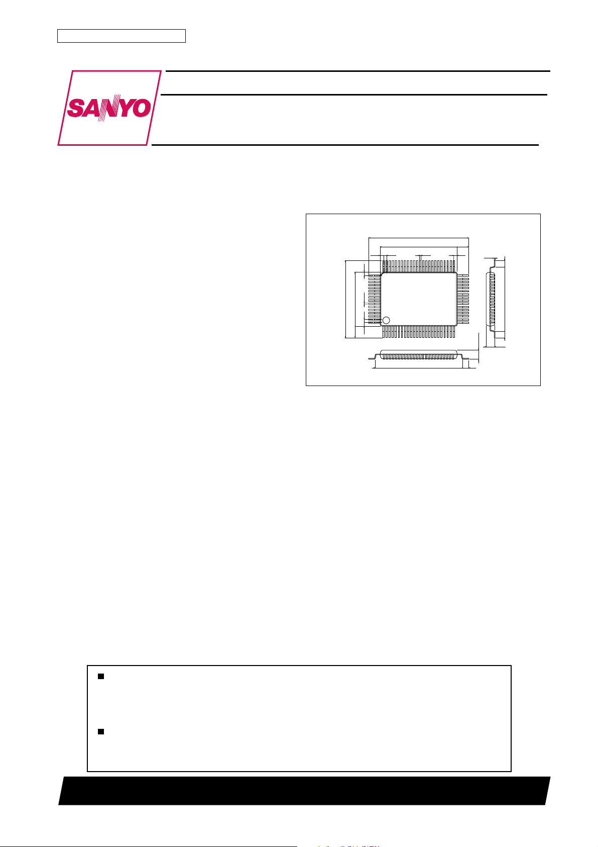
Package Dimensions
unit:mm
3044B-QIP80A
[LC7230-8272]
26.0
20.0
20.0
14.0
3.0
1.0
0.35
0.8
1.0
0.8
0.8
64
65
80
1
0.35
22.6
3.0
0.8
0.15
41
40
25
24
2.45max
1.7
SANYO : QIP80A
1.7
16.6
1.7
2.15
O2501TN (KT)/7251JK/6270TA, (GTPS) No.3100–1/22
Page 2
Functions and Features
• Receiving frequency
Area Band
Japan
USA
EUROPE
S.AFRICA
Receiving Frequency FM (MHz)
Range Others (kHz)
FM
MW
FM
MW
FM
MW
FM
MW
LW
FM
MW
LW
SW
FM
MW
LW
SW
FM
MW
LW
FM
MW
LW
SW
76.0 to 90.0
531 to 1611
(531 to 1629)
87.9 to 107.9
530 to 1610
(530 to 1720)
87.9 to 107.9
522 to 1611
(522 to 1719)
87.50 to 108.00
531 to 1602
(522 to 1611)
153 to 281
(146 to 290)
87.50 to 108.00
531 to 1602
(522 to 1611)
153 to 281
(146 to 290)
SW1 5800 to 7300
SW2 9500 to 18000
87.50 to 108.00
531 to 1602
(522 to 1611)
153 to 281
(146 to 290)
SW1 3200 to 7300
SW2 9500 to 18000
87.50 to 108.00
531 to 1602
(522 to 1611)
153 to 281
(146 to 290)
87.50 to 108.00
531 to 1602
(522 to 1611)
153 to 281
(146 to 290)
SW1 5800 to 7300
SW2 9500 to 18000
LC7230-8272
Reference
Frequency
(kHz)
50
9
(9)
50
10
(10)
50
9
(9)
25
9
(9)
1
(1)
25
9
(9)
1
(1)
5
25
9
(9)
1
(1)
5
5
25
9
(9)
1
(1)
25
9
(9)
1
(1)
5
Step
(kHz)
100
9
(9)
200/100
10
(10)
200/100
9
(9)
50
9
(9)
1
(1)
50
9
(9)
1
(1)
5
50
9
(9)
1
(1)
5
5
50
9
(9)
1
(1)
50
9
(9)
1
(1)
5
FM (MHz)
IF
Others (kHz)
–10.7
450/468
10.7
450
10.7
450/468
10.7
450/468
450/468
10.7
450/468
450/468
450
10.7
450/468
450/468
450
–10.7
450/468
450/468
–10.7
450/468
450/468
450
(↑)
(↑)
(↑)
(↑)
(↑)
(↑)
(↑)
(↑)
(↑)
(↑)
(↑)
(↑)
(↑)
Diode
Matrix
B2B1B
0
1 0 0
0 0 0
1 1 1
0 0 1
0 1 0
0 1 1
↑
1 1 0
1 0 1
Note) 1. A frequency in ( ) is selected by using diode matrix “SHIFT”.
2. The presence or absence of LW and U.S.A. 200/100 are selected by using diode matrix “LW200”.
3. AM IF450/468 is selected by using diode matrix.
• Tuning method (Sawtooth wave mode : )
· Manual up/down
· Auto up/down
· Preset call by 8-button method
• Preset memory
FM: Mode 1 ....... 8 channels
Mode 2 ....... 8 channels 24 channels in all
AM : (MW+LW+SW)
No distinction between mode 1 and mode 2 ......8 channels
• Auto preset scan
• Timer function
· Timer.................. Causes turn-ON mode only. Sleep timer (Set to the nearest 10 minutes).
· Clock.................. 12/24hr mode 12hr : Japan, USA
24hr : Europe, South Africa
• Usable with remote control
The LC7461M-8103 is used.
• Usable with electronic volume control : 7-dot LED (using the LB1417) display available.
The LC7535 is used.
• Usable with the function switch : LCD display and LED (using the MLC74HC375) display available.
The LC7821 (N) is used.
Continued on next page.
No.3100–2/22
Page 3
LC7230-8272
Continued from preceding page.
• On-chip LCD driver : 1/2 duty 1/2 bias frame frequency 100Hz
• Single 5V supply
• Package : QIP80A
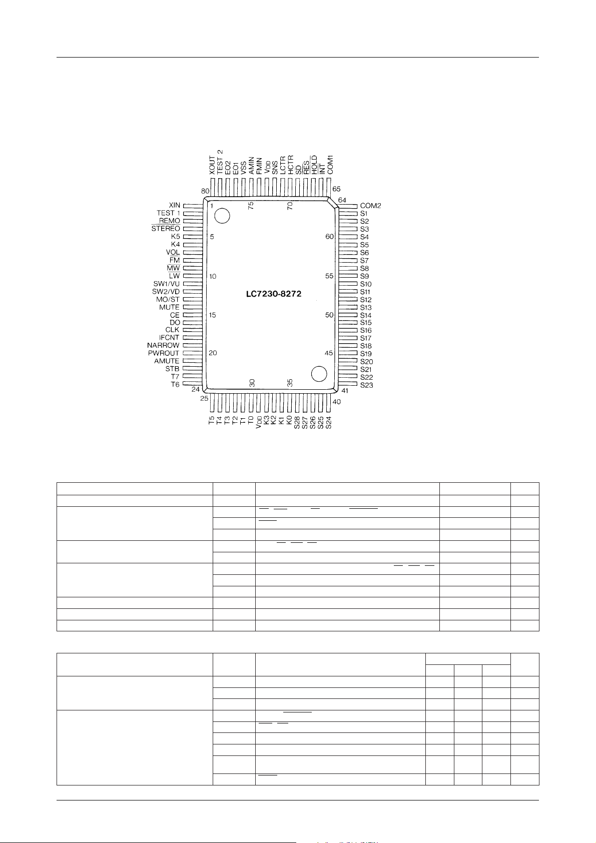
Pin Assignment
Top view
Specifications
Absolute Maximum Ratings at Ta = 25˚C, VSS=0V
retemaraPlobmySsnoitidnoCsgnitaRtinU
egatlovylppusmumixaMV
egatlovtupnI
egatlovtuptuO
tnerructuptuO
noitapissidrewopelbawollAxamdP 004Wm
erutarepmetgnitarepOrpoT 58+ot04–
erutarepmetegarotSgtsT 521+ot54–
Recommended Operating Conditions at Ta = –40 to +85˚C, VDD=3.5 to 5.5V
retemaraPlobmySsnoitidnoC
egatlovylppuS
egatlovlevel-hgihtupnI
xam 5.6+ot3.0–V
DD
VNI14K,5K,OERETS,OMER,DS,SNS,SER,TNI 5.6+ot3.0–V
VNI2DLOH 31+ot3.0–V
VNI3VnahtrehtostupnI
V
1WL,WM,MF,LOV 51+ot3.0–V
TUO
V
2VnahtrehtostuptuO
TUO
I
1WL,WM,MF,LOV,BTS,ETUMA,TUORWP,WORRAN 5ot0Am
TUO
I
2ETUM,TS/OM,DV/2WS,UV/1WS,TNCFI,KLC,OD,EC 3ot0Am
TUO
I
37Tot0T 1ot0Am
TUO
Ta=–40 to +85˚C
VDD1edomgnitarepoLLP
VDD2deppotsLLP,edomgnitarepoKCOLC
VDD3dlohyromeM
V
1HI
V
2HI
V
3HI
V
4HI
V
5HI
V
6HI
TNI,SER
SNS5.25.5V
3K,2K,1K,0K
ETUM
DLOH
V,1NI2Vot3.0–
NI
1Vot3.0–
TUO
1*
2*
3*
4K,5K,OERETS,OMER
,TS/OM,DV/2WS,UV/1WS,TNCFI,KLC,OD,EC
3.0+V
DD
3.0+V
DD
˚C
˚C
sgnitaR
nimpytxam
5.45.5V
5.35.5V
3.15.5V
V7.0
DD
V8.0
DD
V6.0
DD
V7.0
DD
V8.0
DD
5.5V
5.5V
V
DD
V
DD
0.8V
V
V
Continued on next page.
tinU
No.3100–3/22
Page 4
LC7230-8272
Continued from preceding page.
retemaraPlobmySsnoitidnoC
V
1LI
V
2LI
egatlovlevel-woltupnI
ycneuqerftupnI
edutilpmatupnI
egnaregatlovtupnIV
V
V
V
fNI1NIX0.45.40.5zHM
fNI2V,NIMF
fNI3V,)edomWL,WM(NIMA
fNI4V,)edomWS(NIMA
fNI5V,)FIMF(RTCH
fNI6V,)FIMA(RTCL
VNI1NIX05.05.1smrV
VNI2NIMF01.05.1smrV
VNI4,3)edomWL,WM(NIMA01.05.1smrV
VNI6,5RTCL,RTCH01.05.1smrV
NI
SNS03.1V
3LI
4LI
5LI
7DS0V
3K,2K,1K,0K0
ETUM
V,2DD101031zHM
NI
Refer to the item “Relationship of set type, power source and current” for *1, *2, and *3.
Electrical Characteristics / under the allowable operating conditions
retemaraPlobmySsnoitidnoC
htdiwsiseretsyHV
htdiwesluptcejeRP
tnerruclevel-hgihtupnI
tnerruclevel-woltupnI
egatlovgnitaolftupnIV
ecnatsisernwod-lluPR
)hgih(tnerrucegakaeletats-FFOtuptuO
)wol(tnerrucegakaeletats-FFOtuptuO
egatlovlevel-hgihtuptuO
egatlovlevel-woltuptuO
H
JER
IHI1
IHI2V,NIX
IHI3V,RTCL,RTCH,NIMA,NIMF
IHI4V,3K,2K,1K,0K
ILI1VIV=
ILI2VIV=
ILI3VIV=
FI
DP
I
1V,2OE,1OE
HFFO
I
2
HFFO
I
3V
HFFO
I
1V,2OE,1OE
LFFO
I
2
LFFO
VHO1I,7Tot0T
VHO2
VHO3I:2OE,1OE
VHO4I:TUOX
VHO5I:82Sot1S
VHO6I:BTS,ETUMA,TUORWP,WORRAN
VHO7I:2MOC,1MOC
VLO1I,7Tot0T
VLO2
VLO3I:2OE,1OE
VLO4I:TUOX
VLO5I:82Sot1S
VLO6I:BTS,ETUMA,TUORWP,WORRAN
VLO7I:2MOC,1MOC
VLO8I:WL,WM,MF,LOV
SNS 05sµ
V,4K,5K
I
IV=DD
SS
SS
SS
3K,2K,1K,0K
3K,2K,1K,0K57001002kΩ
OV=DD
LO
OV=SS
O
I:DV/2WS
O
O
O
O
O
I:DV/2WS
O
O
O
O
4K,5K,OERETS,OMER0
DLOH,TNI,SER0
V,4DD15.001zHM
NI
V,5DD10.204zHM
NI
V,6DD14.021zHM
NI
V,7DD1001005zHk
NI
TNI,DLOH,SERV1.0
V5.5=
V0.5=0.20.551Aµ
IV=DD
IV=DD
DV/2WS,UV/1WS
Am1=
Am1=
Aµ002=
O
Am1=5.00.10.2V
Am1=
Aµ002=0.1V
O
V0.5=05Aµ
V:DV/2WS,UV/1WS
OV=DD
V,WL,WM,MF,
V31=0.5Aµ
O
Aµ005=
Am1.0–=
Aµ02=
Aµ005=0.1V
Am1.0=0.1V
Aµ02=53.05.07.0V
Am5=
O
,OERETS,OMER,SNS,DS,SER,DLOH,TNI
V0.5=0.40103Aµ
,WORRAN,TUORWP,ETUMA,BTS,7Tot0T
,TS/OM,ETUM,EC,OD,KLC,TNCFI
,WORRAN,TUORWP,ETUMA,DTS,7Tot0T
,TS/OM,ETUM,EC,OD,KLC,TNCFI
,UV/1WS,TS/OM,ETUM,EC,OD,KLC
Am5=
O
,UV/1WS,TS/OM,ETUM,EC,OD,KLC
Am5=0.1V
O
sgnitaR
nimpytxam
,TS/OM,DV/2WS,UV/1WS,TNCFI,KLC,OD,EC
VDD0.2–VDD0.1–VDD5.0–
VDD0.1–
VDD0.1–
VDD0.1–
VDD0.1–
VDD0.1–
VDD7.0–VDD5.0–
0
sgnitaR
nimpytxam
DD
0.20.551Aµ
0.40103Aµ
10.001An
10.001An
VDD53.0–
57.0
051( Ω)
Continued on next page.
V3.0
DD
V2.0
DD
V2.0
DD
V3.0
DD
DD
03Aµ
0.3Aµ
V50.0
DD
0.3Aµ
0.3Aµ
0.1V
0.2
004( Ω)
tinU
V
V
V
V
V
tinU
V
V
V
V
V
V
V
V
V
V
No.3100–4/22
Page 5
LC7230-8272
Continued from preceding page.
retemaraPlobmySsnoitidnoC
egatlovlevel-dimtuptuOV
tnerrucylppuS
Refer to the item “Relationship of set type, power source and current” for *4, *5, and *6.
1V,2MOC,1MOC
M
IDD1VDDf,1
IDD2
IDD3
NI
V
DD
V
DD
V
DD
)2.giF,edom
Fig. 1 IDD2 at HOLD Mode
I,V0.5=
DD
5*)1.giF,edomDLOH
)2.giF,edompukcaB(
Aµ02=0.25.20.3V
O
52=aT,deppotsCSO,V5.5=°6*,C
52=aT,deppotsCSO,V5.2=°pukcaB(,C
4*edomgnitarepoLLP,zHM031=25152Am
,deppotsLLP(edomgnitarepoKCOLC,2
Note) Pins 7 to 30, PH, S1 to S28,
sgnitaR
nimpytxam
23Am
COM1, 2 : Open
tinU
5Aµ
1Aµ
Fig. 2 IDD3 at Backup Mode
Set function grouping
noitcnuF
rellortnocetomeR
kcolcdnaremiT
emulovcinortcelE
hctiwsnoitcnuF
egasuhctiwstcaTegasuhctiwslacinahceM
°
°
°
°
WSREWOP
×
×
°
°
Relationship of set type, power source and current
sutatS
teS
kcolchtiW
tcathctiwsrewoP
kcolctuohtiW
lacinahcemhctiwsrewoPkcolctuohtiW
edomoidaR
nosi
VDD1
IDD1
VDD1
IDD1
VDD1
IDD1
nosirewopnehW
VDD2
IDD2
VDD2
IDD2
VDD2
IDD2
nahtrehtO
edomoidar
VDD2
IDD2
VDD2
IDD2
VDD3
IDD3
Note) Refer to the Electrical characteristic reference for VDD1–3
............ Availiable
°
............ Not available
×
rewopnehW
ffosi
CAnehW
VDD3
IDD3
VDD3
IDD3
VDD3
IDD3
Note) K0 to K3, pins 7 to 30, S1 to
S28, COM1, 2 : Open
ffosirewop
No.3100–5/22
Page 6
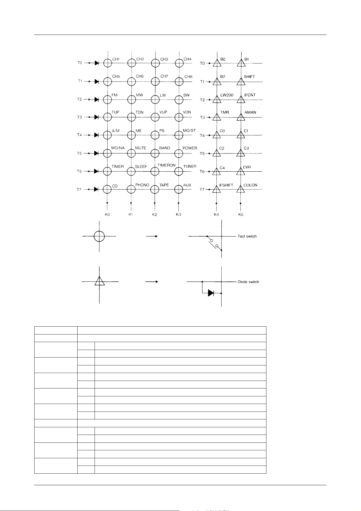
Key Matrix
LC7230-8272
Description of diode matrix (DIMRX) 0 : Without diode 1 : With diode
emaNnoitpircseD
2Bot0B.ycneuqerfgniviecerfotsilehteeS
TFIHS
002WL
TNCFI
RMT
NAMA
4Cot0C)*(=)4C,3C,2C,1C,0C(fognitteS
TFIHSFI
NOLOC
RVE
0)(tuohtiwWS,WL,WMfonoitceleS
1)(niWS,WL,WMfonoitceleS
0srehtorofWLfoecnesba,MFASUrofzH001fonoitceleS
1srehtorofWLfoecneserp,MFASUrofzH002fonoitceleS
0)WLotelbacilppaton(tnuocFItuohtiwgninutotuA
1tnuocFIhtiwgninutotuA
0noitcnufKCOLCremittuohtiW
1noitcnufKCOLCremithtiW
0ylnonoitarepogninutlaunaM
1noitarepogninutlaunam/otuA
0snoitanitsedllarofzHk054ottessiFI)WS,WL,WM(MA
1zHk864ottessi,WM-zHk01dnaWStpecxe,FI)WL,WM(MA
0dethgilsyawlA
1etarzH1atagnihsalF
0elbaliava:edomnoitcerrocremitemulovcinortcelE
1elbaliavaton:edomnoitcerrocremitemulovcinortcelE
* See “Note” in Sample Application Circuit 4 (page 20).
No.3100–6/22
Page 7
LC7230-8272
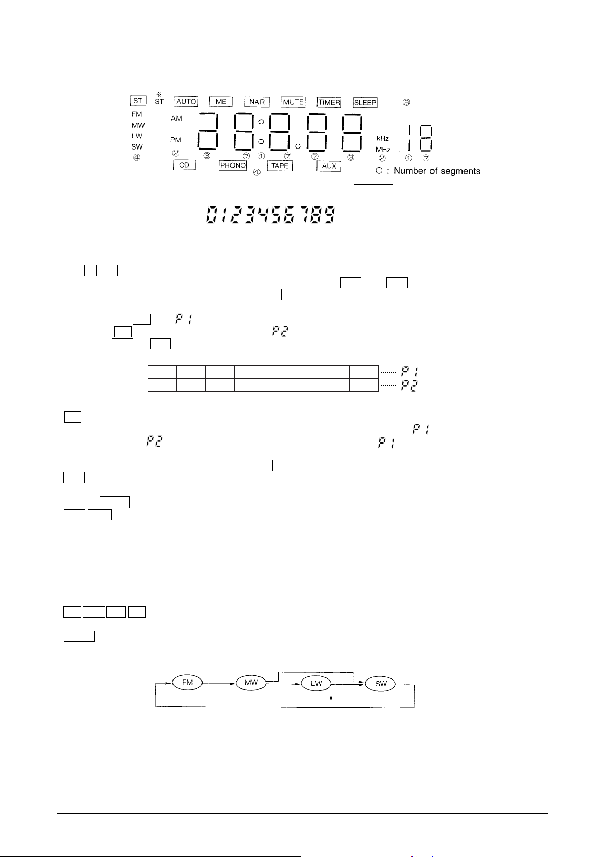
Display
* ST displays when tuned to an FM station and STEREO is held LOW.
Display font
Key Description
• CH1 to CH8
Key for writing/calling preset channels 1 to 16 (FM), 1 to 8 (AM). CH1 key, CH2 key correspond to channel 1/9, 2/
10, respectively. For example, when you push CH1 key and release it within 0.5 second, CH1 is called ; and when
released in 0.5 second or more, CH9 is called.
When you push ME key, is displayed on the frequency display area and CH1 to 8 may be written for 5 seconds.
If you push ME key once again within 5 seconds, is displayed and CH9 to 16 may be written. When you push an y
one key of CH1 to CH8 , your desired channel is written in a specified memory.
CH2 CH3 CH4 CH5 CH6 CH7 CH8
CH1
1
2
3
4
5
6
7
8 channels
(Mode 1)
(Mode 2)
9
10
11
12
13
14
15
8
16
•ME
¡ Used to write a new channel in the preset memory. When you push this key once, (mode 1) is specified. When
you push twice, (mode 2) is specified. When you push once again, returns.
The write enable mode is released automatically 5 seconds after this key pushed.
™ When you push this key together with TIMER key, the timer setting mode (time setting mode) is entered.
• A/M (AMAN DIMRX=1)
Key for selecting the auto/manual tuning mode. Each time you push this ke y, the mode is switched as auto → manual →
auto ..... AUTO display flashes at the auto mode.
• TUP TDN
¡ Manual mode
Each time you push these keys, the channel No. goes up/down by one. When you hold these keys pushed for 500ms
or more, the channel No. goes up/down at a 60ms/step rate.
™ Auto mode (AMAN DIMRX=1)
A broadcasting station is searched automatically in an up/down direction and a receiving frequency is held. If you
hold this key pushed when the receiving frequency is reached, no auto stop occurs but a temporary stop (500ms)
occues. The searching rate is 60ms/step.
• FM MW LW SW
Key for band selection.
• BAND
Key for band selection. Each time you push this key, band switching occurs.
Continued on next page.
No.3100–7/22
Page 8

LC7230-8272
Continued from preceding page.
•PS
Key for preset scanning. When you push this key, the channel No. is changed in the order of increasing channel No.
beginning with a channel No. currently displayed. If no channel No. is displayed, the channel No. is changed from
CH1. If there is a channel that can be received during preset scanning (SD=“L”), a sound is generated for 5 seconds and
if there is no channel that can be received, the channal No. is displayed for 1 second with no sound generated and the
channel No. is changed to the next one. The channel No. flashes at a 1Hz rate during preset scanning.
The preset scanning mode is released by pushing this key twice.
• MO/ST , WD/NA , MUTE
yeKnoitpircseDyalpsiDtuptuO
TS/OM
AN/DW
ETUM
ylnoedomMFtaevitceffE
noitcelesoerets/laruanomroF
ylnoedomMFtaevitceffE
noitcelesdnabworran/ediwroF
.NOrewophtiwsedomllanievitceffE
.detavitcasinwodropuemulovnehwdnaetatsdethgil
ehtgnirudNOrewopotdegnahcsiFFOrewopnehw"L"tuptuodnadethgilnU
TS
RAN
ETUM
dethgiLL
dethgilnUH
dethgiLH
dethgilnUL
dethgiLH
dethgilnUL
•POWER
Switch for turning ON/OFF the power supply of LC7230-8272-applied equipment. Each time you push this key, the
level at output pin PWR OUT is switched as H → L → H ...... The volume level at the power-ON mode is the same as
for the previous power-OFF mode.
• TIMER (Causes turn-ON mode only. Not cause turn-OFF mode “ONCE” timer only.)
Key for providing time display at the timer setting mode, time setting mode or frequenc y display mode . When you push
this key together with ME key, the timer setting mode is entered ; and when you release the two keys once and push
them again simultaneously, the time setting mode is entered.
When you push ME key in the timer setting mode, the timer time setting is enabled with the timer time flashing and the
standby mode is entered. TDN key and TUP key are used for hours setting and minutes setting, respectively. These
settings are made in an up direction only. Each time you push TDN key or TUP key, the display contents increment
by one. When you hold TDN key or TUP key pushed for 500ms or more, the display contents advance at a 4 hours/
second rate or 8 minutes/second rate, respectively.
When you push ME key after completion of setting, a volume lev el at the timer tur ned-ON mode can be set. A digitally
displayed volume level at this moment is the same as for the previously set value. The setting range is from –16dB to
–80dB. The volume level at the initial mode is –50dB.
When you push ME key after completion of setting, the time display mode returns. When you wish to check the set
time only at the timer setting mode, push ME key twice to return the mode to the timer display mode.
Next, in the time setting mode the time setting is enabled with the time display flashing. The setting method is the same
as for the timer setting mode. When you push ME key after completion of setting, the second display is cleared to zero
and the time display mode returns.
When power is turned ON at the initial mode, the time setting mode is entered.
When you push a function key during timer setting or time setting, such mode is released.
Continued on next page.
No.3100–8/22
Page 9

LC7230-8272
• SLEEP
Key for sleep time setting. When you push this k e y in the SLEEP display OFF state, the SLEEP display is turned ON
and (minutes) is displayed. Each time you push this key , decrements in units of 10 minutes. When is reached,
SLEEP display is turned OFF and the sleep time setting mode is released. The previous mode returns 5 seconds after
a sleep time is set to a specified value ( SLEEP key is released).
When you push the SLEEP key while in clock display or frequency display, the remaining sleep time is displayed.
5 seconds after releasing the key the previous status will return.
• TIMER ON
Each time you push this key, TIMER display is turned ON/OFF. When turned ON, the timer operation is carried out ;
and when turned OFF, no timer operation is carried out.
• TUNER
When you push this key in the state where the CD, PHONO, TAPE, AUX functions are provided, the function is
switched to TUNER and the frequency display is provided.
•CD
When you push this key in the state where the PHONO, TAPE, AUX, TUNER functions are provided, data is transferred to the LC7821 (N), the function is switched to CD and CD display is provided. You can also use this key for the
CD power supply control signal and LED function display.
• PHONO
When you push this key in the state where the TAPE, AUX, TUNER, CD functions are provided, data is transferred to
the LC7821 (N), MLC74HC375, the function is switched to PHONO display is provided.
• TAPE
When you push this key in the state where the AUX, TUNER, CD PHONO functions are provided, data is transferred
to the LC7821 (N), MLC74HC375, the function is switched to TAPE , and TAPE display is provided.
•AUX
When you push this key in the state where the TUNER, CD PHONO functions provided, data is transferred to the
LC7821 (N), MLC74HC375, the function is switched to AUX and AUX display is provided.
• VUP VDN
Keys for increasing/decreasing the electronic volume control level. Each time you push these keys, the level goes up/
down by 1dB. When you hold theses keys pushed for 500ms or more, the level goes up/down at a 150ms/dB rate.
The level display for the LB1417 is shown below.
leveLtoDts1toDdn2toDdr3toDht4toDht5toDht6toDht7
noitaunettABd08–Bd25–Bd83–Bd62–Bd81–Bd01–Bd4–
For specifications with no SW band, the volume increase/decrease signal is delivered at the SW1, 2 pins.
Remote Control
(1) The keys other than shown below are the same as for LC7230-8272-applied audio equipment.
emaNyeKnoitpircseDniPmrofevaWtuptuO
ESUAP/YALPDCrofyekESUAP/YALPWORRAN
POTSDCrofyekPOTSTNCFI
TXENDCrofyekTXENWM
KCABDCrofyekKCABWL
PUHC
.1HChtiwstrats.oNlennahc
eslupelgniS
eslupsuounitnoC
7.0rofdehsupyeksihtdlohuoynehW.enoybpuseog.oNlennahceht,yeksihthsupuoyemithcaE
eht,tneserP.oNlennahconsierehtfI.dnoces4.0yrevedehctiwssi.oNlennahceht,eromrodnoces
No.3100–9/22
Page 10

LC7230-8272
(2) Remote control reception interdiction period.
¡ After power on, this unit does not reveive the remote control function for the period in which the volume value
returns from – ∞ to the original value. (When DIMRX of TMR is 1.)
™ After turning the power on, unable to receive for 2 seconds. (When DIMRX of TMR is 0)
Timing Description
(1) Auto up/down mode
IF count tolerance
FM 10.7MHz ±10kHz
MW 450/468kHz ±3kHz
SW 450kHz ±3kHz
LW 450kHz ±600Hz
(2) Manual
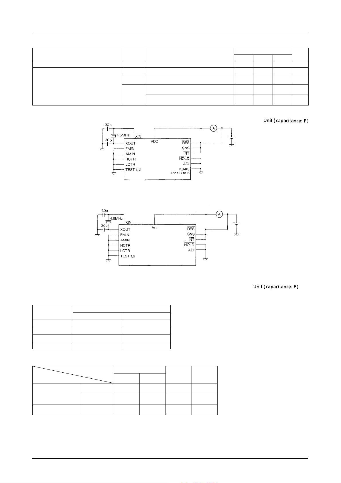
(3) Power ON mode (See Sample Power Supply Connection (1).) (Including the timer, sleep timer modes)
(Note) 1. Data of – ∞ is sent to the LC7535 immediately before power is turned OFF.
2. Data of – ∞ is sent to the LC7535 immediately after power is turned ON.
3. When the SNS pin is brought to H-level after power is turned ON, the original volume level returns at a
38ms/dB rate.
No.3100–10/22
Page 11

LC7230-8272
(4) Audio mute (AMUTE)
¡ Key chattering eliminating time (approximately 40ms)
™ Audio pre-mute time (approximately 50ms)
£ Interstation wait and data transfer to PLL (20ms to 80ms)
¢ Audio post-mute time
§ Processing required for the LC7535, LC7821 (N), MLC74HC375, etc. (approximately 5ms)
a. Band select mode, present channel read mode
b. Manual up/down mode
c. Auto up/down mode
d. PS mode
e. Function select mode (also applicable to FMUTE of the MLC74HC375 (N))
f. Initial power-ON mode
(5) FMUTE (MUTE for Switching Functions)
No.3100–11/22
Page 12

Connection with Peripheral ICs
LC7230-8272
* Note :
CD output and NEXT (MW), BA CK (LW) output when CD function is selected is changed as follo wing. At this time in
order to prevent CD error of point (A), it is necessary to delay CD output.
Pin Description
niP
emaNniP
.oN
NIX1
TUOX08 O
1TSET2
2TSET97
OMER3
OERETS4
LOV7
MF8
WL01tuptuolangisKCABDC
UV/1WS11
DV/2WS21dehsupsiyekNDVnehwylnotuptuo"H"
TS/OM31noitceles"L"oerets/"H"laruanomrofniptuptuOHOB
ETUM41
EC
OD
KLC
TNCFI81
BTS22."LC"otdetcennoC.573CH47CLMehtotatadfoebortsrofniPHOB
51
61
71
.edom
WORRAN91
TUORWP02.niplortnocrewoPHOB
ETUMA12.nipgnitumoiduAHOB
VotdetcennocebtsuM
.–I–
SS
.NOseogthgil
htiW.cepS
dnabWSon
.edomDCehttatuptuo
noitpircseDevitcAO/I
.snipnoitallicsolatsyrczHM5.4–
Votpudellup,esunitonsilortnocetomer
DD
.yalpsidlevellortnocemulov
rewopehttcelesotdesU
.dnabhcaerofylppus
.)N(1287CL,5357CLehtfoenilatadlaireS
onnehW.nipTNIhtiwdesU.niptupnilangislortnocetomeR
cinortceleehtedivorpotnipsihtotdetcennocsi7141BLehT
.tuodeirracsinoitarepoelggot"L"/"H",edomNO-rewopeht
DCehttatuptuolangisPOTS.langisFIehttuptuootlangiS
LI A
.rotsiserahguorht
rotacidniDCL"TS",level-LotthguorbsilangisoeretsehtnehW
LI A
–O C
LO CWM9
tuptuolangisTXENDC
dehsupsiyekPUVnehwylnotuptuo"H"
HO B
tayekETUMhsupuoyemithcaE.edomNO-rewoptalevel-L
HO B
H
HO B
HO B
langisESUAP/YALP."L"dnabediw/"H"dnabworranFIrofniP
HO B
I
O/I
noitarugifnoc
–
Continued on next page.
No.3100–12/22
Page 13

LC7230-8272
Continued from preceding page.
niP
emaNniP
.oN
7T32573CH47LMehtotrefsnartataDEPAT-yalpsidnoitcnuF
6T42573CH47LMehtotrefsnartataDRENUT-yalpsidnoitcnuF
5T52573CH47LMehtotrefsnartataDXUA-yalpsidnoitcnuF
4T62573CH47LMehtotrefsnartataDONOHP-yalpsidnoitcnuF
3T
2T
1T
0T
3K
2K
1K
0K
4K
5K
1S
ot
82S
1MOC
2MOC
DLOH76
DS96.gninutotuagniruddeviecersilennahcatahtmrofniotlangiSLIF
RTCH07.niptupnilangisFIMF–IA
RTCL17.niptupnilangisFIMA–IA
SNS27
NIMF47.OCVMFmorftupniCSOlacoL–IA
NIMA57.OCVMAmorftupniCSOlacoL–IA
TNI66.nipOMERhtiwdesU.niptupnilangislortnocetomeR IA
V
DD
V
SS
SER86VotdetcennocebtsuM
72
82
92
03
23
33
43
53
6
5
36
ot
63
56
46
67
2,1OE
77
13
37
67.DNGotdetcennoC.nipylppusrewoP–––
.langisni-yeKHIA
.langistuptuonacsyeK
.langistupnixirtamedoiDHIA
.sniprevirdtnemgesDCL–OB
.sniprevirdnommocDCL–OD
.detanimilesism02
.–––
DD
noitpircseDevitcAO/I
HO B
.deretnesiedompukcabeht,level-LotthguorbnehW
.detanimilesism02yletamixorppafognirettahcA
,)N(1287CLehtottnessiatad,level-HotthguorbnehW
.langistuptuorotarapmocesahP–OE
.V5+otdetcennoC.nipylppusrewoP–––
LI A
yletamixorppafognirettahcA.7141BL,573CH47CLM,5357CL
HI A
O/I
noitarugifnoc
Pin input/output configuration
Band Power Supply Select Signal
niP
dnaB
MF LH–––
WM HLLLL
WL HLHLL
1WS HLHHL
2WS HLHHH
MFWMWL1WS2WS
No.3100–13/22
Page 14

LC7230-8272
Sample Power Supply Connections
(1) TMR DIMRX “0” “1” function possible.
Use tact switch for power switch (when using the remote control, with timer, etc.)
(2) TMR DIMRX “0” use possible, “1” use not possible.
Use mechanical switch for power switch, (when not using Remote Control, with Timer)
Initial Mode
• Function : TUNER
• Clock 12hr : 12 : 00
24hr : 0 : 00
• Band : FM
• A/M : Manual (AMAN=1)
• Timer, sleep timer : Timer OFF
• Preset channel : None
• ME : OFF
• MO/ST : Stereo MO/ST pin=”L”
• WD/NA : Wide WD/N A pin=”L”
• Volume : –50dB
• Volume level : –50dB
at timer mode
• Muting output : L-level
• PWROUT : L-level
Flashing Timer set value : 10 : 00
No.3100–14/22
Page 15

LC7230-8272
Tracking Point
The following frequencies are loaded in each preset memory at the initial power-ON mode.
aerAdnaB1HC2HC3HC4HC5HC6HC7HC8HC
NAPAJ
ASU
EPORUE
ACIRFA.S
MF0.676.870.386.680.090.670.670.67
WM1353069994041
MF9.781.091.891.6019.7019.789.789.78
WM03500600010041
WM2253069994041
MF5.780.090.890.6010.8015.785.785.78
WL/WM
WS/WM
WS/WM
WS/WL/WM
MF5.780.090.890.6010.8015.785.785.78
WL/WM
WS/WM
WS/WL/WM
135
)225(
↑↑↑↑↑
↑↑↑↑↑
↑↑↑↑↑
135
)225(
↑↑↑↑↑
↑↑↑↑↑
3069994041
3069994041
1161
)9261(
0161
)0271(
1161
)9171(
2061
)1161(
2061
)1161(
135135135
035035035000
225225225111
351
)641(
0085005900531010
0025005900531110
351
)641(
351
)641(
0085005900531
351
)641(
Note 1) ( ) : Value when diode matrix “SHIFT” is selected.
2) CH9 to CH16 are loaded with low band edge at the FM mode.
[FM : MHz, AM : kHz]
072
072
072
072
edoiD
xirtaM
B2B1B
0
001
000
111
100
182
)092(
182
)092(
182
)092(
182
)092(
010
110
010
110
011
101
011
101
No.3100–15/22
Page 16

Waveforms on Segments, Common Pins
LC7230-8272
(1) Connection of Segments on Panel
(2) Connection of Common Pins on Panel
No.3100–16/22
Page 17

LC7230-8272
Sample Application Circuit 1 (With remote controller, timer, function switches and electric volume)
Use tact switch for power switch
No.3100–17/22
Page 18

LC7230-8272
Sample Application Circuit 2 (With remote controller, timer, function switches and electric volume)
Use tact switch for power switch
No.3100–18/22
Page 19

LC7230-8272
Sample Application Circuit 3 (With function switches and electric volume)
Use mechanical switch for power switch
No.3100–19/22
Page 20

Sample Application Circuit 4
LC7230-8272
Note) The above connection of C0-C5 is an experimental
conneciton only.
For mass-production, other specifications authorized
by SANYO Electric Co., Ltd., are required.
.oNYEK.oNYEK.oNYEK.oNYEK
01HC8MF61
12HC9WM71SP52REWOP
23HC01WL81TS/OM62
34HC11WS91PUHC72RENUT
45HC21TXEN02REMIT82DC
56HC31KCAB12PEELS92ONOHP
67HC41PUV22POTS03EPAT
78HC51NDV32ETUM13XUA
YALP
ESUAP
42DNAB
REMIT
NO
No.3100–20/22
Page 21

LC7230-8272
Sample Application Circuit 5 LA1177, LA1266
No.3100–21/22
Page 22

LC7230-8272
Custom Code of the LC7461M-8103
The LC7461M-8103 is a remote control signal transmission IC to be used in conjunction with the LC7230-8272.
The custom code of the LC7461M is such that the 7 bits are fixed by the internal metal mask and the remaining 6 bits are
set using the IC pins.
Custom code 0100H is available for e valuation. When performing evaluation, the code of the LC7461M-8103, LC72308272 must be set to this code value.
When evaluation is acceptable, a custom code to be used must be assigned before mass production of equipment and your
draft on remote control IC should be submitted.
How to set code 0100H for evaluation.
When a custom code for mass production is assigned, C0 to C4 are set to 1 (connected to VDD) or 0 (connected to VSS)
according to the specified code.
Note) A code of the LC7230-8272 is set according to 1 (with diode) and 0 (without diode).
Specifications of any and all SANYO products described or contained herein stipulate the performance,
characteristics, and functions of the described products in the independent state, and are not guarantees
of the performance, characteristics, and functions of the described products as mounted in the customer's
products or equipment. To verify symptoms and states that cannot be evaluated in an independent device,
the customer should always evaluate and test devices mounted in the customer's products or equipment.
SANYO Electric Co., Ltd. strives to supply high-quality high-reliability products. However, any and all
semiconductor products fail with some probability. It is possible that these probabilistic failures could
give rise to accidents or events that could endanger human lives, that could give rise to smoke or fire,
or that could cause damage to other property. When designing equipment, adopt safety measures so
that these kinds of accidents or events cannot occur. Such measures include but are not limited to protective
circuits and error prevention circuits for safe design, redundant design, and structural design.
In the event that any or all SANYO products(including technical data,services) described or
contained herein are controlled under any of applicable local export control laws and regulations,
such products must not be exported without obtaining the export license from the authorities
concerned in accordance with the above law.
No part of this publication may be reproduced or transmitted in any form or by any means, electronic or
mechanical, including photocopying and recording, or any information storage or retrieval system,
or otherwise, without the prior written permission of SANYO Electric Co. , Ltd.
Any and all information described or contained herein are subject to change without notice due to
product/technology improvement, etc. When designing equipment, refer to the "Delivery Specification"
for the SANYO product that you intend to use.
Information (including circuit diagrams and circuit parameters) herein is for example only ; it is not
guaranteed for volume production. SANYO believes information herein is accurate and reliable, but
no guarantees are made or implied regarding its use or any infringements of intellectual property rights
or other rights of third parties.
This catalog provides information as of October, 2001. Specifications and information herein are subject
to change without notice.
PS No.3100–22/22
 Loading...