

Page 1
Ordering number : ENN*6976
83101RM (OT) No. 6976-1/29
Overview
The LC72151V is a PLL frequency synthesizer for car
audio systems. It can implement high-performance
multifunction tuners such as RDS tuners and features a
fast locking circuit.
Functions
• High-speed programmable divider
— FMIN: 10 to 160 MHz: Pulse swallower type
— AMIN: 2 to 40 MHz: Pulse swallower type
0.5 to 10 MHz: Direct division type
• IF counter
— HCTR: 0.4 to 25 MHz: for FM IF count
— LCTR: 10 to 500 kHz: for AM IF count
1.0 to 20 × 103Hz: for frequency
measurement
• Reference frequency
— One of 11 frequencies may be selected (when a
10.25 or 10.35 MHz crystal is used)
50, 30*, 25, 12.5, 10, 9*, 6.25, 5, 3.125, 3*, 1 kHz
Note:
Cannot be used when a 10.25 MHz crystal is
used
• Phase comparator
— Supports dead band control
— Built-in unlock detection circuit
— Built-in deadlock clearing circuit
• Built-in amplifier for forming an active low-pass filter
— Built-in operational amplifier for FM high-speed
locking
— Built-in MOS transistor for AM tuning
• Built-in crystal oscillator output buffer
• I/O ports — General-purpose I/O: 2 pins
— Four input ports (maximum)
— Three output ports (maximum)
• Serial data I/O
— Supports communication with the controller in the
CCB format.
• Operating ranges
— Supply voltage: 4.5 to 5.5 V (VDD)
7.5 to 9.5 V (AVDD)
— Operating temperature: –40 to +85°C
• Package
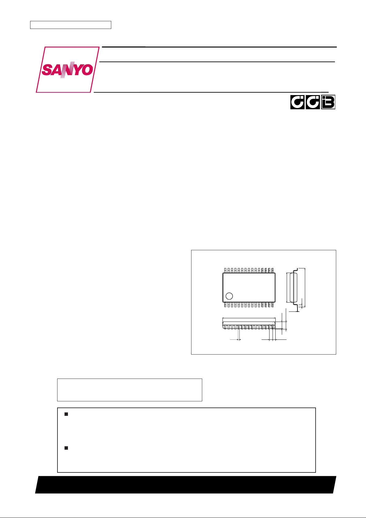
— SSOP30
Package Dimensions
unit: mm
3191A-SSOP30
151
1630
9.75
0.5
7.6
5.6
0.1
(1.3)
1.5max
0.65 (0.43)
0.22
0.15
Preliminary
SANYO: SSOP30
[LC72151V]
LC72151V
SANYO Electric Co.,Ltd. Semiconductor Company
TOKYO OFFICE Tokyo Bldg., 1-10, 1 Chome, Ueno, Taito-ku, TOKYO, 110-8534 JAPAN
PLL Frequency Synthesizer for Electronic Tuning
in Car Audio Systems
CMOS IC
Any and all SANYO products described or contained herein do not have specifications that can handle
applications that require extremely high levels of reliability, such as life-support systems, aircraft’s
control systems, or other applications whose failure can be reasonably expected to result in serious
physical and/or material damage. Consult with your SANYO representative nearest you before using
any SANYO products described or contained herein in such applications.
SANYO assumes no responsibility for equipment failures that result from using products at values that
exceed, even momentarily, rated values (such as maximum ratings, operating condition ranges, or other
parameters) listed in products specifications of any and all SANYO products described or contained
herein.
• CCB is a trademark of SANYO ELECTRIC CO., LTD.
• CCB is SANYO’s original bus format and all the bus
addresses are controlled by SANYO.
Page 2
No. 6976-2/29
LC72151V
Pin Assignment
LC72151
(Top view)
V
XIN
DO
XOUT
I/O-1
I/O-2
S
1 30
2
3
4
5
6
7
8
9
10
11
12
29
28
27
26
25
24
23
22
21
20
XBUF
O-3
V
DD
V
SS
FMIN
AMIN
AV
DD
AV
SS
AOUT1
CL
AOUT2
PDM2
PDF
PDM1
AIN2
PDS
TGI1
TGO
TGI2
AIN1
13
14
+
–
15
19
18
17
16
HCTR/I-3
LCTR/I-4
DI
CE
AREF
S
S
AV
SS
Page 3
No. 6976-3/29
LC72151V
Block Diagram
PDS
PDF
AV
DD
AV
SS
AOUT1
AIN1
AREF
PDM1
AMIN
HCTR/I-3
V
DD
V
SS
TGI2
FMIN
XOUT
XIN
UNIVERSA L
COUNTER
FAST LOCK UP
CONTROL
UNLOCK
DETECTOR
REFERENCE
DIVIDER
PHASE DETECTOR
CHARGE PUMP
DATA SHIFT REGISTER
LATCH
12bits PROGRAM MABL E
DIVIDER
SWALLOW COUNTER
1/16,1/17 4bits
POWER
ON
RESET
CCB
I/F
PDS
TGI1
CL DO I/O-1 I/O-2
CHARGE PUMP
for FAST LOCK
TGO
CE DI O-3
PDM2
AOUT2
AIN2
LCTR/I-4
XBUF
Page 4
No. 6976-4/29
LC72151V
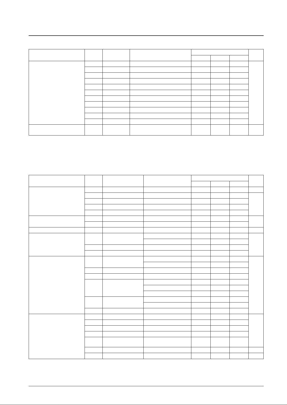
Parameter Symbol Pin Ratings Unit
Supply voltage V
DD
max
V
DD
* –0.3 to +7.0
V
AV
DD
* –0.3 to +11.0
V
IN
1 max CE, CL, DI –0.3 to +7.0
V
IN
2 max
XIN, FMIN, AMIN, HCTR/I-3, LCTR/I-4,
–0.3 to VDD+ 0.3
Maximum input voltage
AIN2, TGI1, TGI2, TGO
V
V
IN
3 max I/O-1, I/O-2 –0.3 to +15.0
V
IN
4 max AIN1, AREF –0.3 to +6.5
V
O
1 max DO –0.3 to +7.0
V
O
2 max
XOUT, PDM1, PDM2, PDS, PDF, XBUF, TGI1,
–0.3 to VDD+ 0.3
Maximum output voltage
TGI2, TGO
V
V
O
3 max I/O-1, I/O-2, O-3, AOUT2 –0.3 to +15.0
V
O
4 max AOUT1 –0.3 to +11.0
I
O
1 max I/O-1, I/O-2, O-3 0 to 10.0
Maximum output current I
O
2 max DO, TGI1, TGI2, TGO, AOUT1, AOUT2 0 to 5.0 mA
I
O
3 max XBUF 0 to 3.0
Allowable power dissipation Pd max (Ta ≤ 85°C) SSOP30 :160 mW
Operating temperature Topr –40 to +85 °C
Storage temperature Tstg –55 to +125 °C
Specifications
Absolute Maximum Ratings at Ta = 25°C, VSS= AVSS= 0 V
Note: Power must be applied to AVDDbefore applying to VDDand AVDDmust be higher than or equal to VDD.
Parameter Symbol Pin Conditions
Ratings
Unit
min typ max
VDD1 V
DD
VDD≤ AV
DD
4.5 5.5
Supply voltage V
DD
2 AV
DD
VDD≤ AV
DD
7.5 8.5 9.5 V
V
DD
3 V
DD
Serial data retention voltage 2.0
V
IH
1 CE, CL, DI 0.7V
DD
6.5
High-level input voltage
V
IH
2 I/O-1, I/O-2 0.7V
DD
13
V
V
IH
3
HCTR/I-3,
0.7V
DD
V
DD
LCTR/I-4
CE, CL, DI,
Low-level input voltage V
IL
I/O-1, I/O-2,
0 0.3V
DD
V
HCTR/I-3,
LCTR/I-4
V
O
1 DO 0 6.5
Output voltage
V
O
2 AOUT1 0 9.5
V
V
O
3
I/O-1, I/O-2, O-3,
0 13
AOUT2
f
IN
1 XIN VIN1 *
1
7 11
f
IN
2 FMIN VIN2 *
1
10 160
f
IN
3 AMIN (SNS=1) VIN3 *
1
2 40 MHz
Input frequency f
IN
4 AMIN (SNS=0) VIN4 *
1
0.5 10
f
IN
5 HCTR/I-3 VIN5 *
1
0.4 25
f
IN
6 LCTR/I-4 VIN6 *
1
10 500 kHz
f
IN
7 LCTR/I-4 VIN7 *
2
1.0 20 × 10
3
Hz
Allowable Operating Ranges at Ta = –40 to 85°C, VSS= AVSS= 0 V
Continued on next page.
Page 5
No. 6976-5/29
LC72151V
Parameter Symbol Pin Conditions
Ratings
Unit
min typ max
V
IN
1 XIN fIN1 200 1500
V
IN
2-1 FMIN f = 10 to 50 MHz 40 1500
V
IN
2-2 FMIN f = 50 to 130 MHz 20 1500
V
IN
2-3 FMIN f = 130 to 160 MHz 40 1500
V
IN
3 AMIN (SNS=1) fIN3 40 1500
Input amplitude V
IN
4 AMIN (SNS=0) fIN4 40 1500 mVrms
V
IN
5-1 HCTR/I-3 f = 0.4 to 25 MHz *
3
40 1500
V
IN
5-2 HCTR/I-3 f = 8 to 12 MHz *
4
70 1500
V
IN
6-1 LCTR/I-4 f = 10 to 400 kHz *
3
40 1500
V
IN
6-2 LCTR/I-4 f = 400 to 500 kHz *
3
20 1500
V
IN
6-3 LCTR/I-4 f = 400 to 500 kHz *
4
70 1500
Guaranteed crystal oscillator
X’tal XIN, XOUT *
5
10.25 10.35 MHz
frequency ranges
Notes: 1. Sine wave with capacitor coupled.
2. Pulse wave with DC coupled.
3. Serial data: CTC = 0
4. Serial data: CTC = 1
5. Recomended CI value for the crystal oscillator: CI ≤ 70 Ω
Continued from preceding page.
Parameter Symbol Pin Conditions
Ratings
Unit
min typ max
Rf1 XIN 1 MΩ
Rf2 FMIN 500
Internal feedback resistance Rf3 AMIN 500
kΩ
Rf4 HCTR/I-3 500
Rf5 LCTR/I-4 500
Internal pull-down resistance
Rpd1 FMIN 80 200 600
kΩ
Rpd2 AMIN 80 200 600
Hysteresis V
HIS
CE, CL, DI, LCTR/I-4 0.1 V
DD
V
V
OH
1 PDM1, PDM2, PDS, PDF
I
O
= – 1 mA VDD– 1.0
High-level output voltage
I
O
= – 2 mA VDD– 2.0
V
V
OH
2 AOUT1 IO= – 1 mA AVDD– 1.0
V
OH
3 XBUF IO= – 0.5 mA VDD– 1.5
V
OL
1 PDM1, PDM2, PDS, PDF
I
O
= 1 mA 1.0
I
O
= 2 mA 2.0
V
OL
2 AOUT1 IO= 1 mA 1.0
V
OL
3 XBUF IO= 0.5 mA 1.5
Low-level output voltage
I
O
= 1 mA 0.2
V
V
OL
4 I/O-1, I/O-2, O-3 IO= 5 mA 1.0
I
O
= 8 mA 1.6
V
OL
5 DO
I
O
=1 mA 0.2
I
O
= 5 mA 1.0
V
OL
6 AOUT2 IO= 1 mA, AIN2 = 1.3 V 0.5
I
IH
1 CE, CL, DI VI= 6.5 V 5.0
I
IH
2 I/O-1, I/O-2 VI= 13 V 5.0
I
IH
3 HCTR/I-3, LCTR/I-4 VI= V
DD
5.0
µA
High-level input current
I
IH
4 XIN VI= V
DD
0.11 0.9
I
IH
5
FMIN, AMIN, HCTR/I-3,
VI= V
DD
1.8 15
LCTR/I-4
I
IH
6 AIN1, AREF VI= 5.5 V 0.01 100 nA
I
IH
7 TGI1, TGI2, TGO VI= V
DD
3.0 µA
Electrical Characteristics in the Allowable Operating Ranges
Continued on next page.
Page 6
No. 6976-6/29
LC72151V
Parameter Symbol Pin Conditions
Ratings
Unit
min typ max
I
IL
1 CE, CL, DI VI= 0 V 5.0
I
IL
2 I/O-1, I/O-2 VI= 0 V 5.0
I
IL
3 HCTR/I-3, LCTR/I-4 VI= 0 V 5.0
µA
Low-level input current
I
IL
4 XIN VI= 0 V 0.11 0.9
I
IL
5
FMIN, AMIN, HCTR/I-3,
VI= 0 V 1.8 15
LCTR/I-4
I
IL
6 AIN1, AREF VI= 0 V 0.01 100 nA
I
IL
7 TGI1, TGI2, TGO VI= 0 V 3.0 µA
V
IN
= 8.5 V, I = ±3 mA,
70 140
AV
DD
= 8.5 V
Analog switch on resistance R
ON
TGI1, TGI2, TGO
V
IN
= 4.5 V, I = ±3 mA,
50 100 Ω
AV
DD
= 8.5 V
V
IN
= 0.5 V, I = ±3 mA,
70 140
AV
DD
= 8.5 V
I
OFF
1 AOUT1 VO= 6.5 V 5.0
Output off leakage current I
OFF
2 I/O-1, I/O-2, O-3, AOUT2 VO= 13 V 5.0 µA
I
OFF
3 DO VO= 6.5 V 5.0
High-level 3-state off leakage current
I
OFFH
PDM1, PDM2, PDS, PDF VO= V
DD
0.01 200 nA
Low-level 3-state off leakage current
I
OFFL
PDM1, PDM2, PDS, PDF VO= 0 V 0.01 200 nA
Input capacitance C
IN
FMIN 6 pF
X’tal = 10.35 MHz
IDD1 V
DD
fIN2 = 160 MHz 10 18
V
IN
2 = 40 mVrms
PLL block stopped
I
DD
2 V
DD
(PLL INHIBIT)
0.5 1.5
X’tal OSC operating mA
Supply current
(X’tal = 10.35 MHz)
PLL block stopped
I
DD
3 AV
DD
(PLL INHIBIT)
1.5
X’tal OSC stopped
On-chip op-amp stopped
PLL block stopped
I
DD
4 V
DD
(PLL INHIBIT)
10 µA
X’tal OSC stopped
On-chip op-amp stopped
Continued from preceding page.
Page 7
No. 6976-7/29
LC72151V
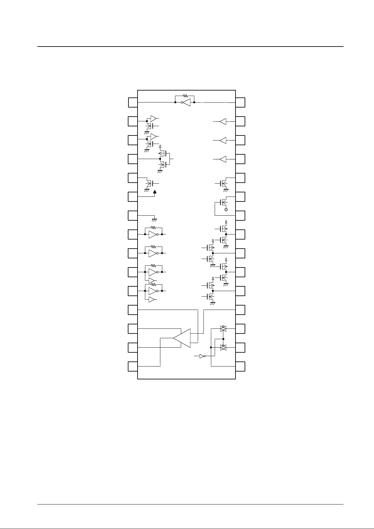
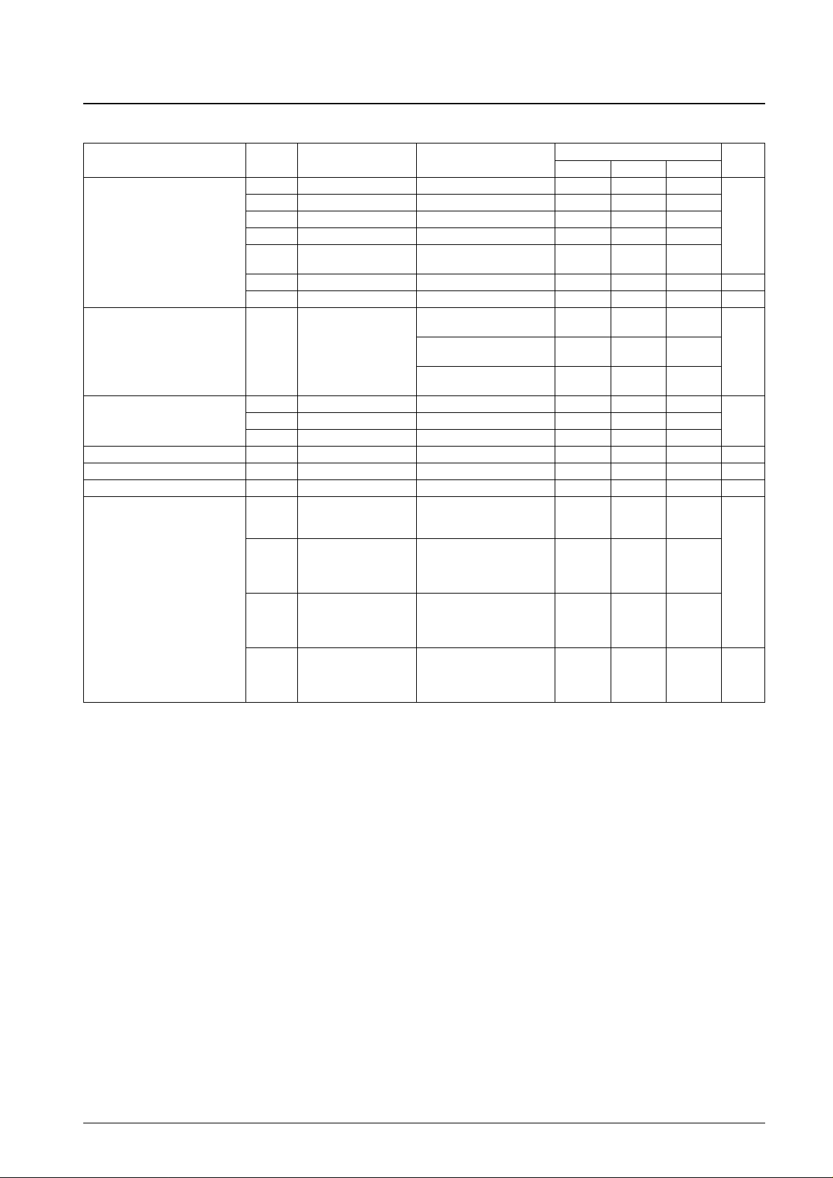
Pin Functions
Pin No. Symbol Usage Function Pin circuit
• Crystal oscillator connection.
(10.25 or 10.35 MHz)
30
1
XIN
XOUT
X’tal OSC
• FMIN is selected by setting DVS in the control data to 1.
• Enters high-speed locking mode by setting SNS in the control data
to 1.
• Enters normal mode by setting SNS in the control data to 0.
• Input frequency: 10 to 160 MHz
• The signal is transmitted to the swallow counter.
• The divisor can be set to a value in the range 272 to 65,535.
8 FMIN Local oscillator signal input
• AMIN is selected by setting DVS in the control data to 0.
• When SNS in the control data is set to 1:
Input frequency: 2 to 40 MHz
The signal is directly transmitted to the swallow counter.
• When SNS in the control data is set to 0:
Input frequency: 0.5 to 10 MHz
The signal is directly transmitted to the 12-bit programmable divider.
The divisor can be set to a value in the range 5 to 4,095.
9 AMIN Local oscillator signal input
• This pin must be set to the high level when inputting serial data to the
LC72151V DI pin and when outputting serial data from the DO pin.
29 CE Chip enable
S
• Serial data input for transferring data from the controller to the
LC72151V.
28 DI Input data
S
• Data synchronization clock signal used when inputting serial data to
the LC72151V DI pin and when outputting serial data from the DO pin.
27 CL Clock
S
• Serial data output for transferring data from the LC72151V to the
controller.
26 DO Output data
• LC72151V power supply. A voltage in the range 4.5 to 5.5 V must be
provided when the PLL circuit is operating.
• The power-on reset circuit operates when power is first applied.
Note: Power must be applied to AV
DD
before applied to VDDand
AV
DD
must be higher than or equal to VDD.
———
———
6
V
DD
Power
• LC72151V ground.7
V
SS
Ground
• Input/output dual function pins
• The function will be selected according to IOC1 and IOC2 in the
control data.
Data = 0: Input port
1: Output port
• When specified as an input port:
The input pin state is transmitted to the system microcontroller from
DO pin.
Input state = Low: data is 0
= High: data is 1.
• When specified as an output port:
The output state will be determined according to I/O-1 and I/O-2 in
the control data.
Data = 0: Low
= 1: Open
• These pin function as an input port at a power-on reset.
2
3
I/O-1
I/O-2
I/O ports
Continued on next page.
Page 8
No. 6976-8/29
LC72151V
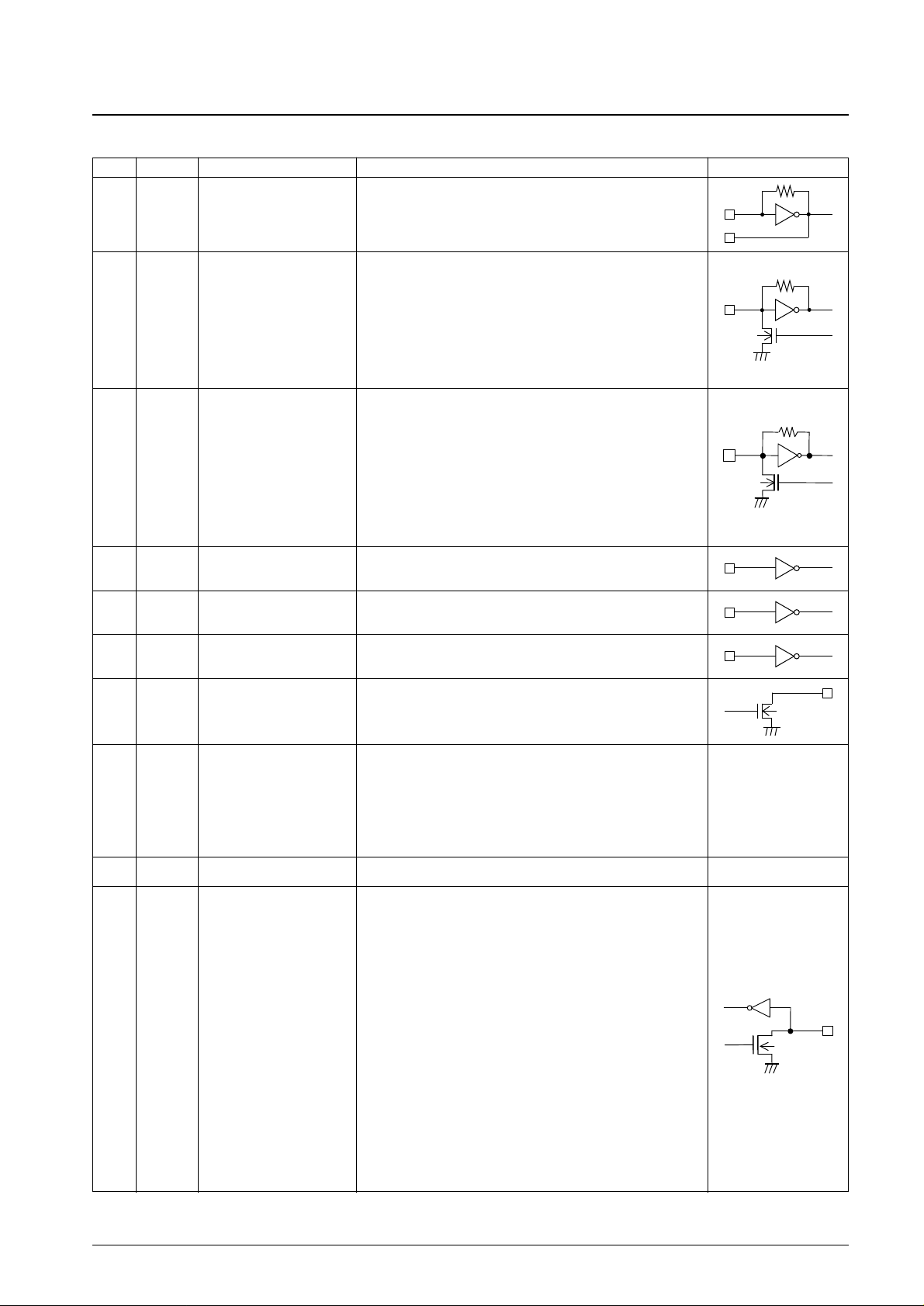
Continued from preceding page.
Pin No. Symbol Usage Function Pin circuit
• Dedicated output pin
• Latches OUT3 in the control data and outputs data from O-3 pin.
• This pin goes open state at a power-on reset.
5 O-3 Output port
• Op-amp for PLL active low-pass filter
• AV
SS
is the analog system ground pin shared with low-pass filter Nch
MOS transistor.
• Voltage applied to AREF pin must be 1/2 that to VDDpin.
Note: Power must be applied to AV
DD
before applied to VDD, and AV
DD
must be higher than or equal to VDD.
19
12
13
14
15
AIN1
AREF
AV
DD
AV
SS
AOUT1
Op-amp for low-pass filter amp
AREF
AIN1
+
–
AOUT1
AV
SS
AV
DD
• PLL active low-pass filter Nch MOS transistor
• Source of the transistor is connected to AV
SS
pin.
Note: Connect AV
SS
pin to ground in use.
24
25
AIN2
AOUT2
Transistor for low-pass
filter amp
AV
SS
• PLL charge pump output
When the frequency created by dividing the local oscillator signal
frequency by N is higher than the reference frequency, a high level is
output from the PD pin. When lower, a low level is output. The PD pin
goes to the high-impedance state when the frequencies match.
21
23
20
PDM1
PDM2
PDS
Charge pump output
• PLL high-speed locking charge pump output
When the high-speed locking mode is selected, signal pulses is
output according to the frequency variation. This pin enters highimpedance state when the local oscillation frequency enters the set
frequency range.
22 PDF
PLL high-speed locking charge
pump output
• PLL high-speed locking active low-pass filter transmission gate
input/output dual function pins
Note: Connect AVSSpin to ground in use.
18
17
16
TGI1
TGI2
TGO
PLL high-speed locking TG
TGO
TGI2
TGI1
• HCTR is selected by setting CTS1 in the control data to 1.
Input frequency: 0.4 to 25 MHz
The signal is input to a divide-by-2 circuit and the result is input to a
general-purpose counter. This counter can also be used as an
integrating counter.
The counter value is output as the result of the count, MSB first, from
the DO pin.
There are four measurement periods: 4, 8, 32, and 64 ms.
• When H/I-3 in the control data is set, this pin functions as an input
port, and the value is output from the output pin DO.
10 HCTR/I-3 General-purpose counter
• LCTR is selected by setting CTS1 in the control data to 1.
• When the LCTR is selected as described above and CTS0 is set to 1:
This pin enters the frequency measurement mode.
Input frequency: 10 to 500 kHz
The signal is directly transmitted to the general-purpose counter.
• When CTS0 is set to 0
This pin enters period measurement mode.
Input frequency: 1 Hz to 20 kHz
Period can be measured either in single period or in double period. If
double period measurement is selected, the frequency is 2 Hz to
40 kHz.
The counter value is output as the result of the count, MSB first, from
the DO pin.
• When L/I-4 in the control data is set:
This pin functions as an input port, the value is output from the output
pin DO.
11 LCTR/I-4 General-purpose counter
Continued on next page.
Page 9
Serial Data I/O Methods
Data is input to and output from the LC72151V using the Sanyo CCB (Computer Control Bus) format, which is the serial
bus format used by SANYO audio ICs. This IC adopts a CCB format with an 8-bit address.
No. 6976-9/29
LC72151V
I/O mode
Address
Content
B0 B1 B2 B3 A0 A1 A2 A3
• Control data input (serial input) mode.
[1] IN1 (82) 0 0 0 1 0 1 0 0
• 32 bits of data are input.
• See the “DI Control Data (Serial Data Input) Structure” item for details on the content of
the input data.
• Control data input (serial input) mode.
[2] IN2 (92) 1 0 0 1 0 1 0 0
• 32 bits of data are input.
• See the “DI Control Data (Serial Data Input) Structure” item for details on the content of
the input data.
• Data output (serial data output) mode.
[3] OUT (A2) 0 1 0 1 0 1 0 0
• The number of bits output is equal to the number of clock cycles.
• See the “DO Output Data (Serial Data Output) Structure” item for details on the content
of the output data.
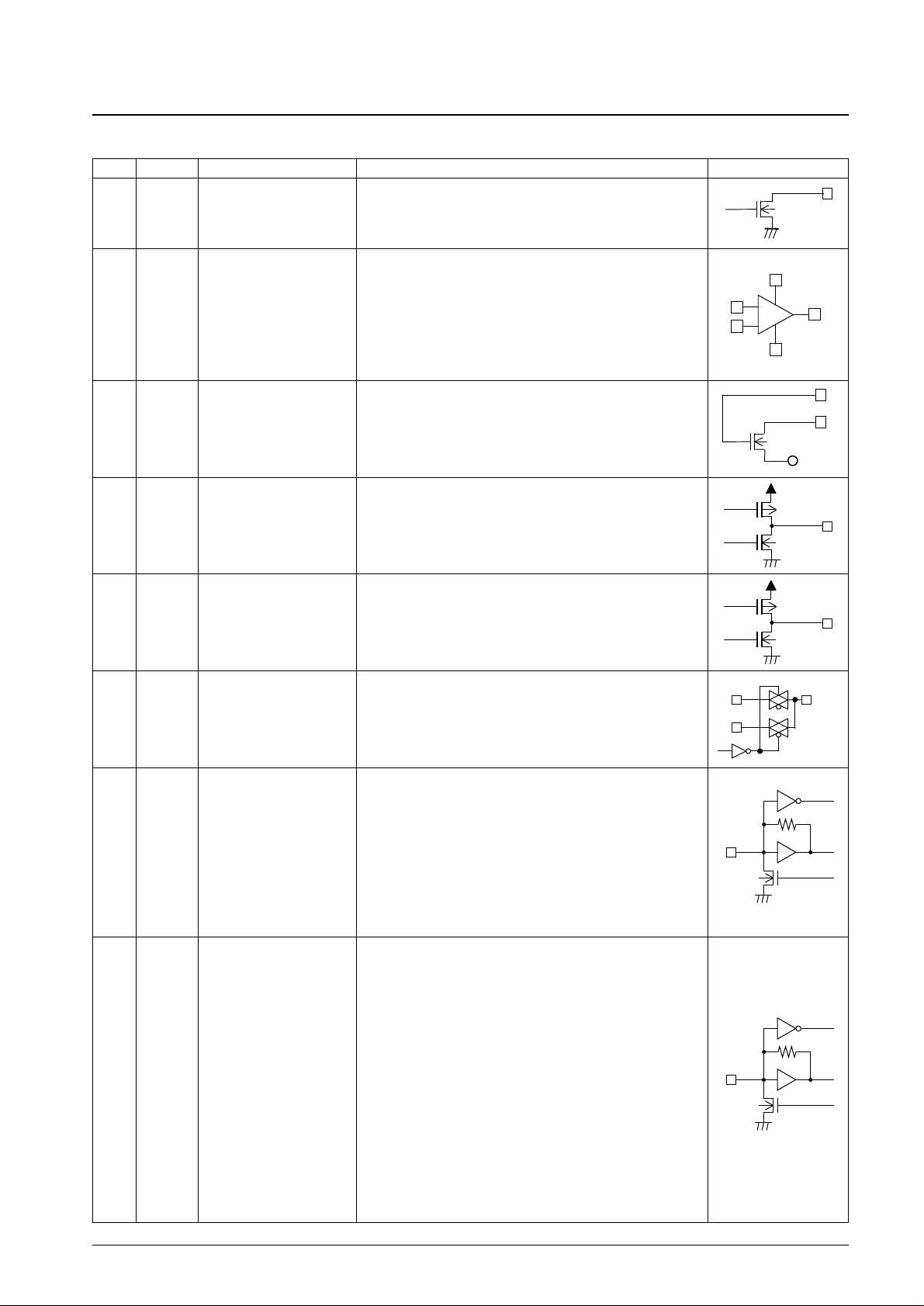
Continued from preceding page.
Pin No. Symbol Usage Function Pin circuit
• Output buffer for the crystal oscillator circuit
• When XB in the serial data is set to 1, the output buffer operates and
the crystal oscillator signal (a pulse signal) is output.
When XB is 0, XBUF outputs a low level.
After the power-on reset, the output buffer is fixed at the low level.
4 XBUF Crystal oscillator buffer
XOUT
CE
1
CL
2
I/O mode determined
DO
A3A2A1A0B3B2B1B0DI
Fir
st Data IN1/2
1
First Data OUT
2
First Data OUT
CL: Normally Hi
1
2
CL: Normally Low
Page 10

DI control data (serial data input) structure
(1) IN1 mode
No. 6976-10/29
LC72151V
R2
R1
R0
PDC1
PDC0
DVS
SNS
P15
P14
P13
P12
P11
P10
(16) Reset
(5) U-CTR
(4) DO-C
(3) R-CTR
(2) PD-C
(1) P-CTR
P9
P8
P7
P6
P5
P4
P3
P2
P1
P0
R3
0010100DI
Address
Address
* : Don’t care
0
GT0
CTS1
CTS0
CTE
RST
DT1
DT0
GT1
UL1
UL0
ULD
IL1
IL0
L/I-4
H/I-3
HSE1
HSE0
CWS1
CWS0
TLR1
TLR0
XS
XB
OUT3
OUT2
OUT1
I/O
*
*
*
-2
I/O-1
0010100DI 1
TEST2
TEST1
TEST0
DZ1
DZ0
DLC
TEST3
(18) XTAL
(17) Don't Care
(15) TEST
(11) DZ-C
(10) PD-L
(9) Unlock
(4) DO-C
(8) U/I-C
(5) U-CTR
(14) HSTMR
(13) CWS-D
(12) TLR-D
(7) O-PORT
(6) I/O-C
CTC
CTP
(17) Don't Care
(2) IN2 mode
Page 11

No. 6976-11/29
LC72151V
DI control data description
No. Control block/data Content Related data
• This data sets the divisor for the programmable divider and P15 is the MSB of this binary
value. LSB will change according to the DVS and SNS.
*: When the LSB is P4, P0 to P3 are invalid.
• Used to select programmable divider signal input pins (FMIN, AMIN) and to switch the
input frequency range.
*: When the DVS and SNS are set to 1, the high-speed locking mode is selected, the high-
speed control data becomes valid.
By setting DVS to 1 and SNS to 0 this pin enters FMIN mode, the sub-charge pump
control data is valid, the high-speed locking control data becomes invalid.
(1)
Programmable divider data
P0 to P15
DVS, SNS
• This data controls the sub-charge pump.
(* : don’t care)
• The sub-charge pump can be used in conjunction with the PDM1 or the PDM2 pin (main
charge pump pin) to form a high-speed locking circuit.
*: FMIN(High-speed mode): Setting DVS and SNS to 1 forces the sub-charge pump to
operate for the time set due to the high-speed locking end flag output wait time, and
allows the locking time to be reduced after switching to the normal PLL mode.
See the “Charge Pump Structure” item for details.
HSE0
HSE1
(2)
Sub-charge pump control data
PDC0, PDC1
• Reference frequency selection data
Note: PLL inhibit (backup mode)
The programmable divider block is stopped, the FMIN and AMIN pins are pulled down
to ground, and the charge pump output is set to the floating state.
(3)
Reference divider data
R0 to R3
PDC1 PDC0 Sub-charge pump state
0 * High impedance
1 1 Charge pump operating (at all times)
1 0 Charge pump operating (when PLL unlocked)
DVS SNS LSB Set divisor (N)
1 1 P0 272 to 65535
1 0 P0 272 to 65535
0 1 P0 272 to 65535
0 0 P4 4 to 4095
DVS SNS Input pin Input pin frequency range
1 1 FMIN 10 to 160 MHz (High-speed mode)
1 0 FMIN 10 to 160 MHz (Normal mode)
0 1 AMIN 2 to 40 MHz
0 0 AMIN 0.5 to 10 MHz
R3 R2 R1 R0 Reference frequency (kHz)
0 0 0 0 50
0 0 0 1 50
0 0 1 0 25
0 0 1 1 25
0 1 0 0 12.5
0 1 0 1 6.25
0 1 1 0 3.125
0 1 1 1 3.125
1 0 0 0 10
1 0 0 1 9
1 0 1 0 5
1 0 1 1 1
1 1 0 0 3
1 1 0 1 30
1 1 1 0 PLL inhibit + X’tal OSC stop
1 1 1 1 PLL inhibit
Continued on next page.
Page 12

No. 6976-12/29
LC72151V
Continued from preceding page.
No. Control block/data Content Related data
• Data that determines the output of the DO pin
*Note: Open state will be selected at the power-on reset.
Note: *1. end-UC: General-purpose counter operation completion check
However, if I/O-1 and I/O-2 are set to output mode, they change from IN to the open
state.
*: DO pin state during data input (IN1, IN2 modes, CE = high) keeps open regardless of the
DO pin control data.
In addition, Do pin during data input (OUT mode, CE = high) outputs the value for the
internal DO serial data synchronized with the CL regardless of the DO pin control data.
Caution: Cannot be used in crystal oscillator stop mode: R0 = 0, R1 = R2 = R3 = 1 (The DO
pin will not change state.)
(1) When the count operation starts by setting end-UC with CTE set to 1 from 0, DO pin
automatically goes to open state.
(2) When the general-purpose counter operation ends, the DO pin goes low, it is allowed to
check the count end.
(3) DO pin goes to open state according to the serial data input/output state: CE pin = high.
(4)
DO pin control data
ULD
DT0, DT1
IL0, IL1
CTE
I/O-1
I/O-2
ULD DT1 DT0 DO pin
0 0 0 Low when unlocked
0 0 1 Open
0 1 0 end-UC *
1
0 1 1 IN *
2
1 0 0 Open
1 0 1 Open
1 1 0 end-UC *
1
1 1 1 IN *
2
IL1 IL0 IN
0 0 Open
0 1 I-1 (pin state)
1 0 I-2 (pin state)
1 1 DO goes low when I-1 changes.
Continued on next page.
Note: *2.
DO
(1) Start (2) Completion (3) CE: HI
Page 13

No. 6976-13/29
LC72151V
No. Control block/data Content Related data
• Selects the general-purpose counter input pins (HCTR, LCTR).
• General-purpose counter measurement start data
CTE = 1: Starts the counter.
CTE = 0: Resets the counter.
• Determines the measurement time (frequency mode) and number of periods (period
mode).
• When CTE = 0, input pull-down is disabied by setting CTP to 1
Note: Wait time: 1 to 2ms.
However, CTP must be set to 1 4ms before CTE is set to 1.
• The input sensitivity is reduced when CTC is set to 1. (Sensitivity: 10 to 30 mV rms)
*: Refer to the General-purpose counter stracture on page 22 for details.
(5)
General-purpose counter
control data
CTS0, CTS1
CTE
GT0, GT1
CTP
CTC
• Data that specifies the I/O direction of the I/O ports (I/O-1, I/O-2).
[Data] = 0: Input port
1: Output port
*: After the power-on reset, the I/O-1 and I/O-2 are set up as input ports.
OUT1, OUT2(6)
I/O port control data
IO-1, I/O-2
• Data that determines the output from output ports O-1 to O-3.
[Data] = 0: Open
1: Low
*: Invalid when the corresponding port is set up as an input port.
*: At a power-on reset, open state is selected by selling the data to 0
I/O-1, I/O-2(7)
Output port data
OUT1 to OUT3
• Data that switch the function between general-purpose counter and input port.
H/I-3 = 0: I-3 (input port)
1: HCTR (gereal-purpose counter)
L/I-4 = 0: I-4 (input port)
1: LCTR (gereal-purpose counter)
CTS0, CTS1
(8)
General-purpose counter
control data
H/I-3, L/I-4
Continued from preceding page.
Frequency measurement
Period measurement
GT1 GT0
Measurement time
Wait time
mode
CTP = 0 CTP = 1
0 0 4 ms 3 to 4 ms 1 to 2 ms One period
0 1 8 3 to 4 ms 1 to 2 ms One period
1 0 32 7 to 8 ms 1 to 2 ms Two periods
1 1 64 7 to 8 ms 1 to 2 ms Two periods
Continued on next page.
CTS1 CTS0 Input pin Measurement mode
1 * HCTR Frequency
0 1 LCTR Frequency
0 0 LCTR Period
Page 14

No. 6976-14/29
LC72151V
Continued from preceding page.
No. Control block/data Content Related data
• Width selection for the phase error (øE) detection function used to determine the PLL
locked/unlocked state. When a phase error greater than the øE detection width from the
table occurs, the PLL circuit is seen as in the unlocked state.
*: When unlocked, the DO pin goes low and the serial data output is UL = 0.
ULD
DT0, DT1
DVS
SNS
(9)
Unlock state detection data
UL0, UL1
• Controls the phase comparator dead band.
*: The phase comparator operates in DZA mode after the power-on reset. (Recomended
modes: DZD, DZC)
(11)
Phase comparator control data
DZ0, DZ1
• Bit that forcible sets the charge pump output to the low level.
DLC = 1: Low level
DLC = 0: Normal operation
*: If a deadlock occurs due to the VCO control voltage (Vtune) going to zero and stopping
the VCO oscillator, set the charge pump output to the low level and set Vtune to V
CC
to
escape from the deadlocked state (deadlock clearing circuit). Normal operation is
selected after the power-on reset.
(10)
Charge pump control data
DLC
• Data to control the frequency in the convergence range to judge the high-speed locking
control completion. This data is valid when FMIN (high-speed mode) is selected by
setting DVS and SNS to 1.
*:The convergence range is 200 kHz at a power-on reset.
Refer to Description of the High-Speed Locking Control System (P.19) for details.
(12)
High-speed locking convergence
range control data
TLR0, TLR1
UL1 UL0 øE detection width Detection output X’tal
0 0 Stopped Open 10.25 M/10.35 MHz
0 1 0 Directly outputs øE 10.25 M/10.35 MHz
±0.49 µs
øE is extended by
10.25 MHz
0.1 to 0.2 ms.
1 0
±0.49 µs
øE is extended by 10.35 MHz
0.11 to 0.22 ms. (fr = 30/9/3 k)
±0.43 µs
øE is extended by 10.35 MHz (Other
0.1 to 0.2 ms. than fr = 30/9/3 k)
±0.98 µs
øE is extended by
10.25 MHz
0.1 to 0.2 ms.
1 1
±0.97 µs
øE is extended by 10.35 MHz
0.11 to 0.22 ms. (fr = 30/9/3 k)
±0.87 µs
øE is extended by 10.35 MHz (Other
0.1 to 0.2 ms. than fr = 30/9/3 k)
DZ1 DZ0 Dead band mode
0 0 DZA
0 1 DZB
1 0 DZC
1 1 DZD
TLR1 TLR0 Convergence range [kHz]
0 0 50
0 1 100
1 0 150
1 1 200
Continued on next page.
øE
DO
0.1 to 0.22ms
Extended
Unlock state output
Page 15

No. 6976-15/29
LC72151V
Continued from preceding page.
No. Control block/data Content Related data
• Data to control the wait time in the high-speed locking. This data is valid when the FMIN
(high-speed mode) is selected by setting DVS and SNS to 1.
*:The wait time is 20 µs at a power on reset.
Refer to Description of the High-Speed Locking Control System (P.19) for details.
DVS
SNS
(13)
High-speed locking charge wait
time control data
CWS0, CWS1
• Crystal oscillator selection data
XS = 0: 10.25 MHz
= 1: 10.35 MHz
• Crystal oscillator buffer (XBUF)
XB = 0: Buffer output is turned off.
XB = 1: Buffer output is turned on.
*: XB = 0: Buffer output is turned off at a power-on reset.
R0 to R3
(18)
Crystal oscillator circuit
XS
XB
• IC test control data
These bits must be set as follows during normal operation.
TEST0 = 0
TEST1 = 0
TEST2 = 0
TEST3 = 0
*: After the power-on reset, the test data is all set to zero.†
(15)
IC test data
TEST0
TEST1
TEST2
TEST3
CWS1 CWS0 Wait time [µs]
0 0 2.5
01 5
10 10
11 20
• Data to control the wait time after the high-speed locking control completes till the
operation is switched to the normal PLL operation. This data is valid when the FMIN
(high-speed mode) is selected by setting DVS and SNS to 1.
During the wait time, the unlock signal is forcibly output, the sub-charge pump allows to
be operated. Thereby, reduces the locking time after switching to the normal PLL
operation.
*:The wait time is 400 µs at a power on reset.
Refer to Description of the High-Speed Locking Control System (P.19) for details.
DVS
SNS
PDC0
PDC1
(14)
High-speed locking completion
flag output wait time control data
HSE0, HSE1
HSE1 HSE0 Wait time [µs]
00 0
0 1 200
1 0 400
1 1 800
(16)
Reset
RST
• This data resets the LC72151V.
*: After the power is first applied, the power-on reset circuit initializes the IC. However,
the data must be set to 1 to ensure the initialization.
(17)
DNC • Set data to 0
†Note: After power is first applied, the power-on reset circuit initializes the IC. However, the CCB data (RST) must be input to the IC to ensure the
initialization.
Page 16

Structure of the DO Output Data (serial output data)
(3) OUT mode
No. 6976-16/29
LC72151V
C1
C2
C3
(2) UNLOCK
(1) IN-PORT
C4
C5
C6
C7
C8
C9
C10
C11
C12
C13
(3) IF-CTR
C14
C15
C16
C17
C18
C19
UL
C0
0
* * * *
010
Address
101
DO
*: Bits that are set to 0.
DI 0
I1
*
*
*
I2
I3
I4
No. Control block/data Content Related data
• The bits I1 to I4 are set to the latched states of the I/O pins I/O-1 and I/O-2 and the input
pins HCTR/I-3 and LCTR/I-4. These states are latched at the point the IC enters data
output mode.
The pin states are latched regardless of the pin mode (input or output).
I1, I2 ← I/O-1 and I/O-2 pin states
I3, I4 ← HCTR/I-3 and LCTR/I-4 pin states
I/O-1
I/O-2
H/I-3
L/I-4
(1)
I/O port data
I4 to I1
• Data created by latching the value for the unlock detection circuit
UL ← 0: Unlocked
1: Locked or in detection halt mode
UL0
UL1
(2)
PLL unlock data
UL
• Data created by latching the value for the IF counter (20-bit binary counter)
C19 ← MSB of the binary counter
C0 ← LSB of the binary counter
CTE
GT0
GT1
(3)
IF counter binary counter
C19 to C0
Pin state = high: 1
low: 0
Page 17

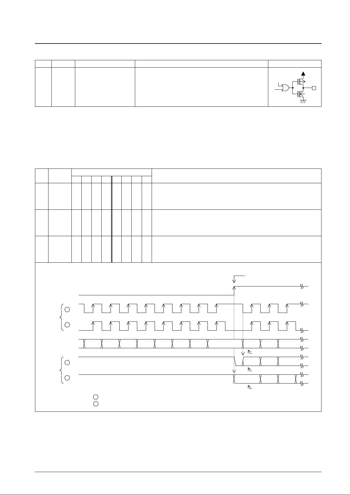
Serial data input (IN1/IN2) tSU, tHD, tEL, tES, tEH, > 0.45 µs tLC< 0.45 µs
No. 6976-17/29
LC72151V
t
LC
t
EH
t
ES
t
EL
t
HD
t
SU
R3R2R1P3P2P1P0A3A2A1A0B3B2B1B0 R0DI
Internal data
Internal data
CE
CL
t
LC
t
EH
t
ES
t
EL
t
HD
t
SU
R3R2R1P3P2P1P0A3A2A1A0B3B2B1B0 R0DI
CE
CL
DO
t
DC
t
DC
t
DH
t
EH
t
ES
t
EL
t
HD
t
SU
I1I3 I2I4
A3A2A1A0B3B2B1B0
C0C1C2C3
DI
CE
CL
DO
t
DC
t
DC
t
DH
t
EH
t
ES
t
EL
t
HD
t
SU
I2I3I4 I1
A3A2A1A0B3B2B1B0
C0C1C2C3
DI
CE
CL
Serial data output (OUT) tSU, tHD, tEL, tES, tEH> 0.45 µs tDC, tDH< 0.2 µs
Note: The DO pin is an n-channel open drain output, and thus the data switching time will differ depending on the value of the pull-up resistor used and the
printed circuit board capacitance.
(1) CL: Normally high
(2) CL: Normally low
(1) CL: Normally high
(2) CL: Normally low
Page 18

No. 6976-18/29
LC72151V
Serial data timing
t
CL
t
EH
t
ES
t
HD
t
SU
t
LC
t
DH
t
DC
t
DC
t
EL
t
CH
V
IL
V
IL
V
IL
V
IH
V
IH
V
IH
V
IH
V
IH
V
IH
V
IL
V
IL
V
IL
DO
Internal
data latch
operation
Old New
Internal
data latch
operation
Old New
CL
DI
CE
t
CH
t
EH
t
ES
t
HD
t
SU
t
LC
t
DH
t
DC
t
EL
t
CL
V
IL
V
IL
V
IH
V
IH
V
IH
V
IH
V
IH
V
IH
V
IL
V
IL
V
IL
DO
CL
DI
CE
<When CL is stopped at the low level>
<When CL is stopped at the high level>
Parameter Symbol Pin Conditions
Ratings
Unit
min typ max
Data setup time t
SU
DI, CL 0.45 µs
Data hold time t
HD
DI, CL 0.45 µs
Clock low-level period t
CL
CL 0.45 µs
Clock high-level period t
CH
CL 0.45 µs
CE wait time t
EL
CE, CL 0.45 µs
CE setup time t
ES
CE, CL 0.45 µs
CE hold time t
EH
CE, CL 0.45 µs
Data latch change time t
LC
0.45 µs
Data output time
t
DC
DO, CL
Depends on the value of the pull-up
0.2 µs
t
DH
DO, CE
resistor used.
Allowable Operating Ranges at Ta = –40 to 85°C, VSS= 0 V
Note: See the timing chart for serial data transfers.
Page 19

Description of the High-Speed Locking Control System
The LC72151V realizes the maximum inter-band edge high-speed locking time 500 µs by optimizing the filter constants
and internal status setting when the FMIN (high-speed mode) by setting DVS and SNS to 1. The following describes the
high-speed locking control system.
Procedure
The LC72151V operates as shown below when selecting FMIN (high-speed mode) and setting sub-charge pump
operation during unlocked.
Control Data
Setting data (CCB) necessary for the new high-speed locking control is described below.
This data is valid when the FMIN (high-speed mode) is selected by setting DVS and SNS to 1.
*: The recommended values are for reference purpose only, not the guarantee values for the fastest locking time.
No. 6976-19/29
LC72151V
Change value N
PDF/PDM1/PDM2/PDS/TGI1/TGI2 pin states
PDF PDM1
*: : operating; : stopped (high-impedance)
PDM2 PDS TGI1 TGI2
→ → →
New high-speed locking control
(When the value N variation is under 16,
only operates the normal PLL.)
Stops the sub-charge pump and only the main-charge
pump operates. (Normal locking state)
Operates normal PLL when the local oscillation frequency
enters the high-speed locking frequency range.
(The sub-charge pump operates for the time set by the
high-speed locking completion flag output wait time.)
CCB data Name (Selectable set value) Description Recommended value
The new high-speed locking control controls the convergence of the
target frequency into the set frequency range.
This data can be used to set the frequency range for convergence
judgement.
*: As the convergence range narrower, the locking time tends to be
shorter.
TLR0 = 0
TLR1 = 0
(±50 kHz)
TLR0/TLR1
High-speed locking convergence range
(±50/100/150/200 kHz)
During the new high-speed locking control, charge application from
the PDF pin and local oscillation frequency measurement for the
FMIN pin are repeatedly implemented.
This data can be used to set the Vt voltage stable time after the
charge is applied until the local oscillator frequency is measured.
*: Voltage stable time Vt changes according to the peripheral
circuit.
CWS0 = 1
CWS1 = 0
(5 µs)
CWS0/CWS1
High-speed locking charge wait time
(0/2.5/5/10 µs)
After the new high-speed locking control ends, since the phase
remains in convergence state in the internal unlock detection circuit
until the locking judgement is implemented, the sub-charge pump
will not operate by the sub-charge pump operation setting during
unlocked.
This data can be used to set the time to force the sub-charge pump
to operate for after the new high-speed locking control completes.
*: After the new high-speed locking control completes, the locking
time tends to be shortened by operating the sub-charge pump for
an adequate time.
HSE0 = 0
HSE1 = 1
(400 µs)
HSE0/HSE1
High-speed locking completion flag output
wait time
(0/100/200/400 µs)
Page 20

Block Diagram
No. 6976-20/29
LC72151V
PDM1
PDM2
Phase
Detector
Unlock
Detector
and
Subcharge
Pump Cont
Unlock
PDS
PDF
Fast Lock Up
Control
Reference Divider
Programmable Divider
Register <value N (New)>
Register <value N (Old)>
Register <Count value>
Frequency Counter
XIN
FMIN
CCB
(CE,DI,CL)
Gate Time
System Clock for Fast Lock Up Control
TGI1
TGI2
TGO
+
–
AV
SS
AREF AIN1 AV
DD
AOUT
VCO
Page 21

Charge Pump Structure
Note: If the unlock state is detected when the channel changes, the sub-charge pump (PDS) operates. Since the sub-
charge pump operates concurrently with the main-charge pump, decrease the time constants for the low-pass filter
to accelerate the locking.
However, note that when the FMIN (high-speed mode) is selected and when the channel changes (during highspeed locking control), both the main- and the sub-charge pumps do not operate and enter the high impedance
state, and forcibly implement an unlock judgement. When locked at a high-speed locking control completion, the
output is not extended but locking is instantaneously judged. By selecting sub-charge operation (during unlocked)
with FMIN (high-speed mode) selected, the sub-charge pump is forcibly operated to shorten the locking time for
the time set by the high-speed locking completion flag output wait time control data (HSE0, HSE1) after switching
from high-speed locking control to normal PLL operation.
No. 6976-21/29
LC72151V
PDM1
(MAIN)
(MAIN)
PDM2
fvco/N
Phase
Detector
Unlock
Detector
and
Subcharge
Pump Cont
fref
Clock Unlock
DZ0
UL0
UL1
PDC0 PDC1
DO
DLC
DZ1
(SUB)
PDS
PD New high-speed
locking charge pump
Main-charge pump
Main-charge pump
Conventional high-speed
locking sub-charge pump
F
(High Speed)
Fast Lock Up
Control
TLR0,TLR1
CWS0,CWS1
HSE0,HSE1
PDC1 PDC0 PDS(Sub-charge pump state)
0 * High impedance
1 1 Charge pump operating (at all times)
1 0 Charge pump operating (when PLL unlocked)
DLC PDM1, PDM2, PDS
0 Normal operation
1 Forced low
Page 22

General-purpose counter structure
No. 6976-22/29
LC72151V
4–7 8–11 12–15 16–190–3
S1
S2
S3
CTS0CTS1
(T)
(FIF)
GT
GT1,GT0
M
S
B
L
S
B
CT
C = FIF × GT
C = (1/T) ÷ 900kHz
E
HCTR
Single period/
double period
extraction circuit
LCTR
1
2
4/8/32/64
ms
DO pin
General-purpose counter
(20-bit binary counter)
I/O signal
switching gate
Check signal
Parameter LCTR period measurement mode check signal frequency
X’tal OSC 10.25 MHz
10.35 MHz
fref = 30, 9, 3 kHz fref = other than 30, 9, 3 kHz
Check signal 1025 kHz 1030 kHz 1150 kHz
CTS1 CTS0 Input pin Measurement mode Frequency range Input sensitivity
S1 1 * HCTR Frequency 0.4 to 25.0 MHz 40 mVrms *
1
S2 0 1 LCTR Frequency 10 to 500 kHz 40 mVrms *
1
S3 0 0 LCTR Period 1.0 to 20 × 103Hz (Pulse)
*1: CTC = 0: 40 mVrms
CTC = 1: 70 mVrms
—: No stipulation ( Not guaranteed)
( ): Actual value (Reference value)
HCTR: Minimum input sensitivity regulation f [MHz]
CTC 0.4 ≤ f < 8 8 ≤ f < 12 12 ≤ f ≤ 25
0 (Normal mode) 40 mVrms
40 mVrms
40 mVrms
(5 to 15 mVrms)
1 (Degrade mode) —
70 mVrms
—
(40 to 60 mVrms)
LCTR: Minimum input sensitivity regulation f [MHz]
CTC 10 ≤ f< 400 400 ≤ f ≤ 500
0 (Normal mode) 40 mVrms
20 mVrms
(1 to 10 mVrms)
1 (Degrade mode) —
70 mVrms
(15 to 30 mVrms)
GT1 GT0
Frequency measurement mode
Period measurement mode
Measurement time Wait time
0 0 4 ms 3 to 4 ms 1 period
0 1 8
1 0 32 7 to 8 ms 2 periods
1 1 64
CTC: Input sensitivity select data. Input sensitivity is degraded by setting CTC to 1.
However, the actual value for HCTR is in the range 40 to 60 mVrms at 10.7 MHz, for LCTR is in the range 15 to
30 mVrms at 450 kHz.
CTP: Input pull-down can be inhibited by setting CTP to 1.
Set CTP to 1 4 ms before setting CTE to 1. Set CTP to 0 when the counter is not used.
Wait time will be reduced to 1 to 2 ms by setting CTP to 1.
Page 23

The LC72151V’s general-purpose counter is a 20-bit binary counter.
The result of the count operation can be read out MSB first from the DO pin.
The measurement time when the general-purpose counter is used for frequency measurement is set to either 4, 8, 32, or
64 ms by the GT0 and GT1 bits. The frequency of the input to the HCTR pin can be measured by determining how many
pulses were input to the general-purpose counter during this measurement time.
When the general-purpose counter is used to measure the frequency, the period of the signal input to LCTR pin can be
measured by counting the number of check signals input to the general-purpose counter for the one or two periods of the
signal input to the LCTR pin.
Reset the general-purpose counter in advance by setting CTE to 0 before starting the counter.
A general-purpose counter count operation is started by setting the CTE bit in the serial data to 1. The serial data takes
effect internally to the LC72151V when the CE pin input level is changed from high to low. The input to the HCTR pin
must be provided before the wait time has elapsed after CE was set low.
Next, the result of the general-purpose counter count after the measurement completes must be read out while CTE is still
set to 1. This is because the general-purpose counter is reset when CTE is set to 1.
Never fail to reset the general-purpose counter before starting the count operation of the general-purpose counter. In
addition, the signal input to LCTR pin is directly transmitted to the general-purpose counter.
Note that the signal input to the HCTR pin is first divided by 2 internally to the IC and then input to the general-purpose
counter. Therefore, the result of the general-purpose counter count is a value that corresponds to 1/2 of the frequency
actually input to the HCTR pin.
No. 6976-23/29
LC72151V
CT
Measurement
time
E=1
CE
GT
end-UC
T : Wait time
WU
t
WU
Start
Completion
Internal data
latch
(CTE)
Generalpurpose
counter
CTE=0
Reset
Start
Res
Integrates
End of the count operation End of the count operation
tart
CTE=1CTE=1
CE
GT
end-UC
(DO)
When used as an integrating counter
In integrating count mode, the count value of the general-purpose counter is accumulated. Care must be taken to handle
counter overflow correctly. The count value will be in the range 0Hto FFFFFH.
• Resets the general-purpose counter
• Starts the general-purpose counter
• Restarts the counter if set to 1 again.
1 →
*CTE: 0 →
Page 24

Other items
(1) Notes on the phase detector dead band
When the charge pump operates in ON/ON mode, the charge pump generates correction pulses even when the PLL is
locked. Here, it is easy for the loop to become unstable, and special care is required in designs that use this mode.
The following problems may occur in ON/ON mode.
• Side bands may be generated due to reference frequency leakage.
• Side bands may be generated due low-frequency leakage due to the envelope of the correction pulses.
No. 6976-24/29
LC72151V
DZ1 DZ0 Dead band mode Charge pump Dead band
0 0 DZA ON/ON – –0 s
0 1 DZB ON/ON –0 s
1 0 DZC OFF/OFF +0 s
1 1 DZD OFF/OFF ++0 s
When a dead band is present (OFF/OFF mode), the loop will be stable, but it will be harder to acquire a good C/N ratio.
On the other hand, with the mode that does not have a dead band (ON/ON mode), it will be easier to acquire a high C/N
ratio, but harder to acquire loop stability.
Therefore, the DZA and DZB modes, in which there is no dead band, can be effective if either a high signal-to-noise ratio
of 90 to 100 dB in FM reception or an increased pilot margin in AM stereo reception is required.
Inversely, if such a high FM signal-to-noise ratio is not required for FM reception, or an adequate pilot margin can be
acquired for AM stereo reception, then the DZC and DZD modes, in which a dead band is present, may be more
effective.
Dead zone (dead band) definition
The phase comparator compares fp with the reference frequency (fr) as shown in figure 1. This circuit outputs a voltage
V (A) that is proportional to the phase difference ø as shown in figure 2. However, due to internal delays and other
factors, the actual IC is unable to compare small phase differences, and thus a dead zone (B) appears in the output. To
achieve a high signal-to-noise ratio in the end product, the dead zone should be as small as possible.
However, in popularly-priced models, there are cases where a somewhat wider dead zone may be easier to work with.
This is because in some situations, such as when a powerful signal is applied to the RF input, in popularly-priced models
there may be RF leakage from the mixer to the VCC. When the dead zone is narrow, outputs to correct this leakage are
output, that output in turn modulates the VCO, and generates a beat signal with the RF.
Reference divider
Programmable divider
VCO
LPF
Phase
detector
MIX
RF
Leakage
fr
fp
ø (nsec)
(B)
(A)
V
Dead zone
Figure 1
Figure 2
(2) Notes on the FMIN, AMIN, HCTR/I-3, and LCTR/I-4 pins
The coupling capacitor must be located as close as possible to these pins. A capacitance of approximately 100 pF is
desirable.
In particular, if the HCTR/I-3 and LCTR/I-4 pin capacitor is over about 1000 pF, the time required to reach the bias level
may become excessive, and incorrect counting may occur due to the relationship with the wait time.
Page 25

(3) Notes on the IF counting using HCTR/I-3 and LCTR/I-4 pins
When counting the IF frequency, the application microcontroller must test the state of the IF IC SD (station detect)
signal, and only if the SD signal is present, turn on the IF counter buffer output and perform an IF count operation.
Methods in which auto-search operations are implemented only using the IF count may incorrectly stop at frequencies
where no station is present due to leakage from the IF counter buffer.
(4) Using the DO pin
At times other than data output mode, the DO pin can also be used to check for general-purpose counter count operation
completion, to output the unlock state detection signal, and to check for changes in the input pins.
Note that the states of the input pins (I/O-1 and I/O-2) can be directly input to the system microcontroller through the DO
pin.
(5) Power supply pins
Capacitors must be inserted between the VDDand VSSpower supply pins and between AVDDand AVSSto reduce noise.
These capacitors must be located as close to the VDDand VSS, AVDDand AVSSpins as possible.
Additionally, power must be applied to AVDDbefore applying to VDD, and AVDDmust be higher than or equal to VDD.
(6) Note on power application
After power is first applied, the power-on reset circuit initializes the IC. However, the CCB data RST must be set to 1 to
ensure the initialization.
(7) Notes on VCO design
The VCO must be designed so that the VCO oscillation does not stop if the control voltage (Vtune) becomes 0 V. If it is
possible for this oscillator to stop, use the charge pump control data (DLC) to forcible set Vtune to VCC temporarily to
prevent the PLL circuit from deadlocking. (This function is called a deadlock clear circuit.)
Pin states during a power-on reset
No. 6976-25/29
LC72151V
LC72151V
XO
State Power-on state
F I-1
F
O
I-2
O: Open L: Low F: Floating
StatePower-on state
UT
I/O-1
I/O-2
XBUF
O-3
V
DD
V
SS
FMIN
AMIN
HCTR/I-3
LCTR/I-4
AREF
AV
DD
AV
SS
AOUT1
XIN
CE
DI
CL
DO
AOUT2
AIN2
PDM2
PDF
PDM1
PDS
AIN1
TGI1
TGI2
TGO
Page 26

No. 6976-26/29
LC72151V
Sample Application Circuit
XIN
DO
XOUT
I/O-1
I/O-2
S
1 30
2
3
4
5
6
7
8
9
10
11
12
29
28
27
26
25
24
23
22
21
20
XBUF
O-3
V
DD
V
SS
AMIN
FMIN
AV
DD
AV
SS
AOUT1
CL
AOUT2
PDM2
PDF
PDM1
AIN2
PDS
TGI1
TGO
TGI2
AIN1
13
14
15
19
18
17
16
LCTR/I-4
HCTR/I-3
DI
CE
AREF
S
S
AMVCO
FMVCO
SD
Tuner-System
ST-Indicate
FM/AM-IF
IF-Request
FM/AM
µ-COM
CE
DI
CL
Unlock
SD
end-UC
U-Count
ST-Indic
DO
2nd Mixer
VCC=8V
V
CC
=8V
VCC=8V
10.25M/10.35MHz
200Ω
8.2kΩ
100Ω
4700pF
2kΩ
0.033µF
10kΩ
22kΩ
100pF
100pF
100pF
330Ω
33pF
100Ω
1000pF
4.3kΩ
5.6kΩ
0.068µF
0.01µF
3.3kΩ
3.9kΩ
AV
SS
*: The constants shown are for reference purpose only, but do not guarantee the operation.
Notes: 1. Power must be applied to AV
DD
before applying to VDD, and AVDDmust be higher than or equal to VDD.
2. AREF is an op-amp reference input voltage pin and must be applied a voltage 1/2 V
DD
. The applied voltage requires to be applied
from another power supply from V
DD
to prevent affections due to logic system noise or other factors.
Page 27

LC72151V State Setting Examples
1. In the case of FMRF 87.5 MHz reception (X’tal = 10.35 MHz/IF = +10.8 MHz)
FM VCO = 98.3 MHz
X’tal = 10.35 MHz, fref = 50 kHz : XS = 1, R0 = R1 = R2 = R3 = 0
FMIN (high-speed mode) selected : DVS = 1, SNS = 1
Dead-zone mode = DZD : DZ0 = DZ1 = 1
Programmable divider divisor
98.3 MHz ÷ 50 kHz = 1966 → 07AE (Hex)
High-speed locking control conditions
High-speed locking convergence range = ±50 kHz : TLR0 = TLR1 = 0
High-speed locking charge wait time = 5 µs : CWS0 = 1, CWS1 = 0
High-speed locking completion flag output wait time = 400 µs : HSE0 = 0, HSE1 = 1
Unlock detection width = ±0.43 µs : UL0 = 0, UL1 = 1
No. 6976-27/29
LC72151V
P0
LSB
First Data IN1
Transmitted data
Transmitted data
10
11DI
8
0
00 000
101101111000001101000000000000
2
P1P2P3P4P5P6P7P8P9
P10
P11
P12
P13
P14
P15
SNS
DVS
PDC0
PDC1
R0R1R2
R3
DT0
DT1
RST
CTE
CTS0
CTS1
GT0
GT1
EA70B000
MSB
I/O-1
LSB
First Data IN2
11
DI
Address
Address
9
1
00 000
0
** ***
*
0 0100010010000000010110000
2
I/O
*
*
*
-2
OUT1
OUT2
OUT3
XB
XS
TLR0
TLR1
CWS0
CWS1
HSE0
HSE1
H/I-3
L/I-4
CTP
CTC
IL0
IL1
ULD
UL0
UL1
DLC
DZ0
DZ1
TEST0
TEST1
TEST2
TEST3
01900D0
MSB
[IN1]
[IN2]
Page 28

No. 6976-28/29
LC72151V
2. In the case of AMRF 530 kHz reception (X’tal = 10.35 MHz/IF = 10.8 MHz)
AM VCO = 11.330 MHz
X’tal = 10.35 MHz, fref = 10 kHz : XS = 1, R0 = R1 = R2 = 0, R3 = 1
X’tal Buffer ON : XB = 1
AMIN selected : DVS = 0, SNS = 1
Dead-zone mode = DZD : DZ0 = DZ1 = 1
Programmable divider divisor
11.330 MHz ÷ 10 kHz = 1133 → 046D (Hex)
P0
LSB
First Data IN1
01
11
DI
8
0
00 000
101110001000001000000100000000
2
P1P2P3P4P5P6P7P8P9
P10
P11
P12
P13
P14
P15
SNS
DVS
PDC0
PDC1
R0R1R2
R3
DT0
DT1
RST
CTE
CTS0
CTS1
GT0
GT1
D 6 4 0 1800
MSB
I/O-1
LSB
First Data IN2
11DI
9
1
00 000
00 1100000000000000010110000
2
I/O-2
OUT1
OUT2
OUT3
XB
XS
TLR0
TLR1
CWS0
CWS1
HSE0
HSE1
H/I-3
L/I-4
CTP
CTC
IL0
IL1
ULD
UL0
UL1
DLC
DZ0
DZ1
TEST0
TEST1
TEST2
TEST3
81000D0
MSB
Address
Transmitted data
Transmitted data
Address
*** * * *
*
*
*
[IN1]
[IN2]
Page 29

PS No. 6976-29/29
LC72151V
This catalog provides information as of August, 2001. Specifications and information herein are subject to
change without notice.
Specifications of any and all SANYO products described or contained herein stipulate the performance,
characteristics, and functions of the described products in the independent state, and are not guarantees
of the performance, characteristics, and functions of the described products as mounted in the customer’s
products or equipment. To verify symptoms and states that cannot be evaluated in an independent device,
the customer should always evaluate and test devices mounted in the customer’s products or equipment.
SANYO Electric Co., Ltd. strives to supply high-quality high-reliability products. However, any and all
semiconductor products fail with some probability. It is possible that these probabilistic failures could
give rise to accidents or events that could endanger human lives, that could give rise to smoke or fire,
or that could cause damage to other property. When designing equipment, adopt safety measures so
that these kinds of accidents or events cannot occur. Such measures include but are not limited to protective
circuits and error prevention circuits for safe design, redundant design, and structural design.
In the event that any or all SANYO products (including technical data, services) described or contained
herein are controlled under any of applicable local export control laws and regulations, such products must
not be exported without obtaining the export license from the authorities concerned in accordance with the
above law.
No part of this publication may be reproduced or transmitted in any form or by any means, electronic or
mechanical, including photocopying and recording, or any information storage or retrieval system,
or otherwise, without the prior written permission of SANYO Electric Co., Ltd.
Any and all information described or contained herein are subject to change without notice due to
product/technology improvement, etc. When designing equipment, refer to the “Delivery Specification”
for the SANYO product that you intend to use.
Information (including circuit diagrams and circuit parameters) herein is for example only; it is not
guaranteed for volume production. SANYO believes information herein is accurate and reliable, but
no guarantees are made or implied regarding its use or any infringements of intellectual property rights
or other rights of third parties.
ZOOM
98.2MHz → 118.7MHz
0.41ms
±10kHz
0.39ms
±10kHz
118.7MHz → 98.2MHz
ZOOM
Locking time (Reference data)
*: Data here are measured using a SANYO evaluation board with the peripheral circuits and state setting shown in the
Sample Application Circuit and the LC72151V State Setting Examples.
 Loading...