

Page 1
Ordering number : ENN6974A
41202RM (OT)/70601RM (OT) No. 6974-
Overview
The LC72148V is a 3 V version of the LC72146 PLL
frequency synthesizer that can easily implement a variety
of 3 V power supply tuners, including in-car navigation
system receivers based on the VICS FM multiplex system.
Functions
• High-speed programmable divider
— FMIN: 10 to 180 MHz
...
Pulse swallower technique
— AMIN: 2 to 40 MHz
...
Pulse swallower technique
0.5 to 10 MHz
...
Direct division technique
• IF counters
— HCTR: 0.4 to 25 MHz
...
Frequency measurement
— LCTR: 10 to 500 kHz
...
Frequency measurement
1.0 to 20 × 103Hz
...
Period measurement
• Reference frequency
— One of 12 reference frequencies can be selected
(Crystal resonator: 7.2 or 4.5 MHz)
1, 3, 5, 9, 10, 3.125, 6.25, 12.5, 25, 30, 50, and
100 kHz
• Phase comparator
— Provides dead zone control
— Built-in unlock detection circuit
— Built-in deadlock clear circuit
— Sub-charge pump for high-speed locking
• Built-in MOS transistor for implementing an active lowpass filter
• I/O ports: Five general-purpose I/O ports.
— Input: 7 pins (maximum)
— Output: 7 pins (maximum. N-channel: 4 pins,
CMOS: 3 pins)
— A clock time base signal (8 Hz) can be output.
• Serial data I/O
— Supports communication with a controller in the
CCB format.
— Uses the same serial data as the LC72146.
• Operating ranges
— Supply voltage: 2.7 to 3.6 V
— Operating temperature: –40 to +85°C
• Package
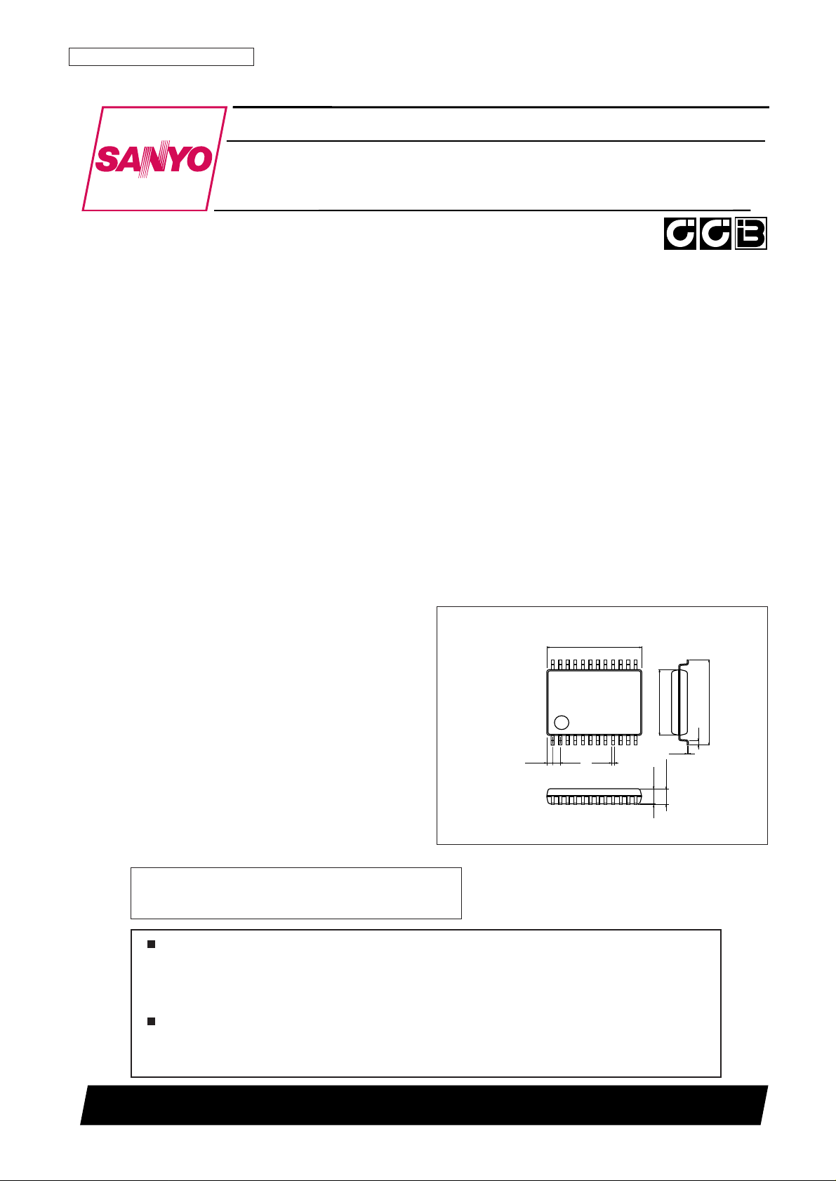
— SSOP24
Package Dimensions
unit: mm
3175B-SSOP24
1
7.6
7.8
0.5
5.6
0.1
1.5max
24
0.65
0.22
(0.33)
0.15
(1.3)
SANYO: SSOP24
[LC72148V]
LC72148V
SANYO Electric Co.,Ltd. Semiconductor Company
TOKYO OFFICE Tokyo Bldg., 1-10, 1 Chome, Ueno, Taito-ku, TOKYO, 110-8534 JAPAN
Electronic Tuning PLL Frequency Synthesizer
for Car Stereo Systems
CMOS IC
Any and all SANYO products described or contained herein do not have specifications that can handle
applications that require extremely high levels of reliability, such as life-support systems, aircraft’s
control systems, or other applications whose failure can be reasonably expected to result in serious
physical and/or material damage. Consult with your SANYO representative nearest you before using
any SANYO products described or contained herein in such applications.
SANYO assumes no responsibility for equipment failures that result from using products at values that
exceed, even momentarily, rated values (such as maximum ratings, operating condition ranges, or other
parameters) listed in products specifications of any and all SANYO products described or contained
herein.
• CCB is a trademark of SANYO ELECTRIC CO., LTD.
• CCB is SANYO’s original bus format and all the bus
addresses are controlled by SANYO.
Page 2
Pin Assignment
No. 6974-2/21
LC72148V
XIN24V
SSa
23
AOUT22AIN21PD020PD119V
SSd
18
FMIN17AMIN16V
DD
15
HCTR/I-614LCTR/I-7
13
XOUT
1CE2DI3CL4DO5
O-76O-6
7
I/O-58I/O-49I/O-310I/O-211I/O-1
12
Block Diagram
XIN
24
XOUT
1
FMIN
17
AMIN
Power on
reset
CCB
I/F
Data shift register latch
12 bits programmable divider
Swallow counter
1/16, 1/17 4 bits
Reference
divider
Phase detector
charge pump
Universal
counter
16
CE
2
DI
3
CL
4
DO
5
V
DD
15
V
SSd
I/O-1
18
V
SSa
23
AOUT
22
AIN
21
LCTR/I-7
13
HCTR/I-6
14
PD0
20
PD1
19
12
I/O-211I/O-310I/O-49I/O-58O-67O-7
6
Page 3
No. 6974-3/21
LC72148V
Parameter Symbol Conditions Ratings Unit
Supply voltage V
DD
max V
DD
–0.3 to +7.0 V
V
IN
1 max CE, CL, DI –0.3 to +7.0 V
Maximum input voltage V
IN
2 max XIN, FMIN, AMIN, HCTR/I-6, LCTR/I-7, AIN, I/O-4, I/O-5 –0.3 to VDD+ 0.3 V
V
IN
3 max I/O-1, I/O-2, I/O-3 –0.3 to +15.0 V
V
O
1 max DO –0.3 to +7.0 V
Maximum output voltage V
O
2 max XOUT, I/O-4, I/O-5, O-6, PD0, PD1, AIN –0.3 to VDD + 0.3 V
V
O
3 max I/O-1, I/O-2, I/O-3, AOUT, O-7 –0.3 to +15.0 V
I
O
1 max I/O-4, I/O-5, O-6, O-7 0 to 3.0 mA
Maximum output current I
O
2 max DO, AOUT 0 to 6.0 mA
I
O
3 max I/O-1, I/O-2, I/O-3 0 to 10 mA
Allowable power dissipation Pd max (Ta ≤ 85°C) SSOP24 140 mW
Operating temperature Topr –40 to +85 °C
Storage temperature Tstg –55 to +125 °C
Specifications
Absolute Maximum Ratings at Ta = 25°C, Vssd = Vssa = 0 V
Parameter Symbol Conditions
Ratings
Unit
min typ max
Supply voltage
V
DD
1 V
DD
2.7 3.6 V
V
DD
2 VDD: Serial data retained 1.5 V
V
IH
1 CE, CL, DI, I/O-1, I/O-2, I/O-3 0.7 V
DD
6.5 V
High-level input voltage V
IH
2 I/O-4, I/O-5, HCTR/I-6, LCTR/I-7 0.7 V
DD
V
DD
V
V
IH
3 LCTR/I-7: Pulse waveform 0.7 V
DD
V
DD
V
Low-level input voltage
V
IL
1
CE, CL, DI, I/O-1 to I/O-5,
0 0.3 V
DD
V
HCTR/I-6, LCTR/I-7
V
IL
2 LCTR/I-7: Pulse waveform 0 0.3 V
DD
V
Output voltage
V
O
1 DO 0 6.5 V
V
O
2 I/O-1, I/O-2, I/O-3, O-7, AOUT 0 13 V
f
IN
1 XIN: VIN1 *
1
1 8 MHz
f
IN
2 FMIN: VIN2 *
1
10 180 MHz
f
IN
3 AMIN (SNS = 1): VIN3 *
1
2 40 MHz
Input frequency f
IN
4 AMIN (SNS = 0): VIN4 *
1
0.5 10 MHz
f
IN
5 HCTR/I-6: VIN5 *
1
0.4 25 MHz
f
IN
6 LCTR/I-7: VIN6 *
1
10 500 kHz
f
IN
7 LCTR/I-7 *
2
1.0 20 × 10
3
Hz
V
IN
1 XIN: fIN1 200 900 mVrms
V
IN
2-1 FMIN: f = 10 to 130 MHz 20 900 mVrms
V
IN
2-2 FMIN: f = 130 to 180 MHz 40 900 mVrms
V
IN
3 AMIN (SNS = 1): fIN3 40 900 mVrms
Input amplitude
V
IN
4 AMIN (SNS = 0): fIN4 40 900 mVrms
V
IN
5-1 HCTR/I-3 (CTC = 0): f = 0.4 to 25 MHz 40 900 mVrms
V
IN
5-2 HCTR/I-3 (CTC = 1): f = 8 to 12 MHz 70 900 mVrms
V
IN
6-1 LCTR/I-4 (CTC = 0): f = 10 to 400 kHz 40 900 mVrms
V
IN
6-2 LCTR/I-4 (CTC = 0): f = 400 to 500 kHz 20 900 mVrms
VIN6-3 LCTR/I-4 (CTC = 1): f = 400 to 500 kHz 70 900 mVrms
Guaranteed operation range for
X’tal XIN, XOUT *
3
4.0 8.0 MHz
crystal resonator
Allowable Operating Conditions at Ta = 25°C, Vssd = Vssa = 0 V
Notes: 1. Sine wave, capacitance coupling
2. Pulse waveform, DC coupling (period measurement)
3. Recommended CI values for the crystal resonator: CI ≤ 120Ω(4.5 MHz) or CI ≤ 70Ω (7.2 MHz)
Page 4
No. 6974-4/21
LC72148V
Parameter Symbol Conditions
Ratings
Unit
min typ max
Rf1 XIN 1 MΩ
Rf2 FMIN 500 kΩ
Internal feedback resistors Rf3 AMIN 500 kΩ
Rf4 HCTR/I-6 250 kΩ
Rf5 LCTR/I-7 250 kΩ
Internal pull-down resistors
Rpd1 FMIN 80 200 600 kΩ
Rpd2 AMIN 80 200 600 kΩ
Hysteresis V
HIS
CE, CL, DI, LCTR/I-7 0.1 V
DD
V
High-level output voltage
V
OH
1
PD0, PD1, I/O-4, I/O-5, O-6, I
O
= –0.5 mA VDD– 0.5 V
PD0, PD1, I/O-4, I/O-5, O-6, I
O
= –1 mA VDD– 1.0 V
V
OH
2 AIN, IO= –5 mA VDD– 1.0 V
V
OL
1
PD0, PD1, I/O-4, I/O-5, O-6, O-7, I
O
= 0.5 mA 0.5 V
PD0, PD1, I/O-4, I/O-5, O-6, O-7, I
O
= 1.0 mA 1.0 V
V
OL
2 AIN, IO= 5 mA 1.0 V
I/O-1, I/O-2, I/O-3, I
O
= 1 mA 0.2 V
Low-level output voltage
V
OL
3
I/O-1, I/O-2, I/O-3, I
O
= 2.5 mA 0.5 V
I/O-1, I/O-2, I/O-3, I
O
= 5 mA 1.0 V
I/O-1, I/O-2, I/O-3, I
O
= 9 mA 1.8 V
V
OL
4 DO, IO= 5 mA 1.0 V
V
OL
5 AOUT, IO= 10 mA, AIN = 2.0 V 1.5 V
I
IH
1 CE, CL, DI, VI= 6.5 V 5.0 µA
I
IH
2 I/O-1, I/O-2, I/O-3, VI= 13 V 5.0 µA
High-level input current
I
IH
3 I/O-4, I/O-5, HCTR/I-6, LCTR/I-7, VI= V
DD
5.0 µA
I
IH
4 XIN, VI= V
DD
1.3 8 µA
I
IH
5 FMIN, AMIN, VI= V
DD
2.5 15 µA
I
IH
6 HCTR/I-6, LCTR/I-7, VI= V
DD
5.0 30 µA
I
IL
1 CE, CL, DI, VI= 0 V 5.0 µA
I
IL
2 I/O-1, I/O-2, I/O-3, VI= 0 V 5.0 µA
Low-level input current
I
IL
3 HCTR/I-6, LCTR/I-7, VI= 0 V 5.0 µA
I
IL
4 XIN, VI= 0 V 1.3 8 µA
I
IL
5 FMIN, AMIN, VI= 0 V 2.5 15 µA
I
IL
6 HCTR/I-6, LCTR/I-7, VI= 0 V 5.0 30 µA
Output off leakage current
I
OFF
1 I/O-1, I/O-2, I/O-3, O-7, AOUT, VO= 13 V 5.0 µA
I
OFF
2 DO, VO= 6.5 V 5.0 µA
High-level three-state off leakage
I
OFFH
PD0, PD1, AIN, VO= V
DD
0.01 200 nA
current
Low-level three-state off leakage
I
OFFL
PD0, PD1, AIN, VO= 0 V 0.01 200 nA
current
Input capacitance C
IN
FMIN 6 pF
I
DD
1
V
DD
, X’tal = 7.2 MHz, fIN2 = 180 MHz, VIN2 = 40 mVrms,
3 8 mA
f
IN
5 = 25 MHz, VIN5 = 40 mVrms
V
DD
, With the PLL block stopped. (PLL INHIBIT)
Supply current I
DD
2 With the crystal oscillator operating. 0.5 1.5 mA
(Crystal frequency = 7.2 MHz)
I
DD
3
V
DD
, With the PLL block stopped.
10 µA
With the crystal oscillator stopped.
Electrical Characteristics for the Allowable Operating Ranges
Page 5
No. 6974-5/21
LC72148V
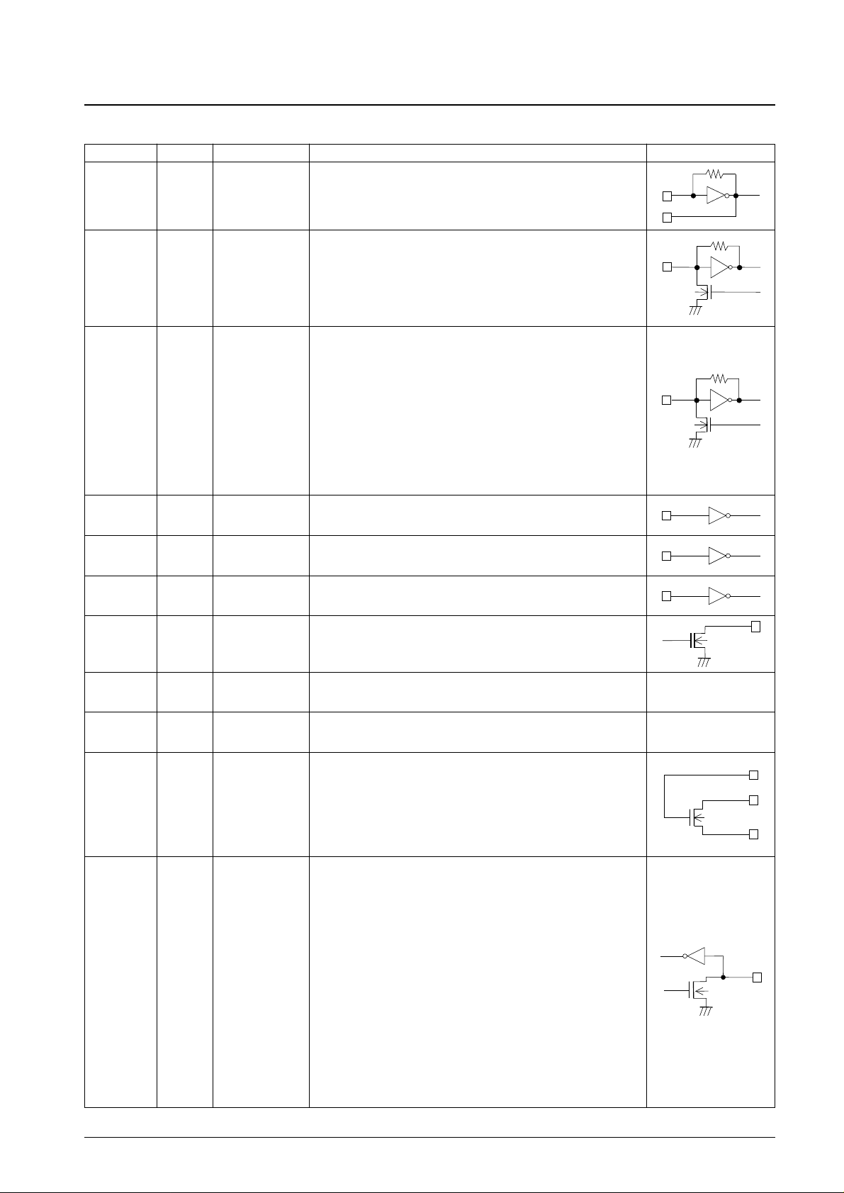
Pin Functions
Pin No. Symbol Type Function Pin circuit
• Crystal resonator connections (7.2 or 4.5 MHz)
XIN
XOUT
24
1
X’tal
• FMIN is selected when DVS in the serial data input is set to 1.
• The input frequency range is 10 to 180 MHz.
• The signal is directly transmitted to the swallow counter.
• The divisor can be set to a value in the range 272 to 65,535.
FMIN17
Local oscillator
signal input
• AMIN is selected when DVS in the serial data input is set to 0.
• When SNS in the serial data input is set to 1:
—The input frequency range is 2 to 40 MHz.
—The signal is directly transmitted to the swallow counter.
—The divisor can be set to a value in the range 272 to 65,535.
• When SNS in the serial data input is set to 0:
—The input frequency range is 0.5 to 10 MHz.
—The signal is directly transmitted to the 12-bit programmable divider.
—The divisor can be set to a value in the range 5 to 4,095.
AMIN16
Local oscillator
signal input
• This pin must be set to the high level during serial data input (DI) from, or
serial data output (DO) to, the LC72148V.
CE2
S
Chip enable
• Input pin for serial data transmitted from the controller to the LC72148V.DI3
S
Input data
• Data synchronization clock used during serial data input (DI) from, or
serial data output (DO) to, the LC72148V.
CL4
S
Clock
• Data output pin for data output from the LC72148V to the controller.
The content of the data output is determined by the ULD, DT0, and DT1
bits in the serial data.
DO5 Output data
• The LC72148V power supply pin. (VDD= 2.7 to 3.6 V)
• The power-on reset circuit operates when power is first applied.
———
———
V
DD
15 Power supply
• Digital system ground for the LC72148V
V
SSd
18 Ground
• Connections to the internal n-channel MOS transistor provided to
implement an active low-pass filter for the PLL.
• A high-speed locking circuit can be implemented by using these pins in
conjunction with the built-in sub-charge pump.
• See the item describing the structure of the charge pump for details.
• Vssa is a dedicated ground pin.
AIN
AOUT
V
SSa
21
22
23
Low-pass filter
amplifier transistor
• Input/output shared-function pins
• In output mode, the circuits are open-drain outputs.
• The I/O direction is determined by I/O-1 to I/O-3 in the serial data.
When the data is 0: input port
When 1: output port
• When specified for use as input ports
The input pin states are transmitted from the DO pin to the controller
Input state = low : Data = 0
Input state = high : Data = 1
• When specified for use as output ports
The output states are determined by OUT1 to OUT3 in the serial data.
Data = 0 : low
Data = 1 : open
• These pins are set to function as input ports by the power-on reset.
I/O-1
I/O-2
I/O-3
12
11
10
General-purpose
I/O ports
Continued on next page.
Page 6
No. 6974-6/21
LC72148V
Continued from preceding page.
Pin No. Symbol Type Function Pin circuit
• Input/output shared-function pins
• In output mode, the circuits are complementary outputs.
• The I/O direction is determined by I/O-4 and I/O-5 in the serial data.
When the data is 0: input port
When 1: output port
• When specified for use as input ports
The input pin states are transmitted from the DO pin to the controller
Input state = low : Data = 0
Input state = high : Data = 1
• When specified for use as output ports
The output states are determined by OUT4 and OUT5 in the serial data.
Data = 0 : low
Data = 1 : high
• These pins are set to function as input ports by the power-on reset.
I/O-4
I/O-5
9
8
General-purpose
I/O ports
• The OUT6 bit in the serial data is latched and output from O-6.O-67 Output port
• The OUT7 bit in the serial data is latched and output from O-7.
• This pin outputs the 8 Hz clock time base signal when TBC is 1.
• This pin is set to the open state by the power-on reset.
O-76
Output port
• PLL charge pump output pins
When the frequency created by dividing the local oscillator signal
frequency by N is higher than the reference frequency, a high level is
output from the PD0 pin, and when lower, a low level is output. When the
frequencies match, PD0 goes to the high-impedance state.
• PD1 operates in a similar manner.
PD0
PD1
20
19
Charge pump
output
• HCTR is selected when CTS1 in the serial data input is set to 1.
—The input frequency range is 0.4 to 25 MHz
—The signal is passed through an internal divide-by-two circuit and
transmitted to a general-purpose counter. An integrating count can also
be performed.
—The result is output starting with the MSB of the general-purpose
counter from the DO pin.
—There are four counting time periods: 4, 8, 32, or 64 ms.
—See the item on the general-purpose counter for details.
• When H/I-6 in the serial data is set to 0
— This pin functions as an input port, and its state is output from the DO
output pin.
HCTR/I-614
General-purpose
counter
• LCTR is selected when CTS1 in the serial data input is set to 0.
• When CTS0 in the serial data input is set to 1 in the CTS1=0 state.
—The circuit operates in frequency measurement mode.
—The input frequency range is 10 to 500 kHz.
—The signal is transmitted directly to the general-purpose counter.
• When CTS0 in the serial data input is set to 0
—The circuit operates in period measurement mode.
—The input frequency range is 1 Hz to 20 kHz.
—The measurement period can be set to be either 1 period or 2 periods.
If 2-period measurement is selected, the input frequency range will be
2 Hz to 40 kHz.
—The result is output starting with the MSB of the general-purpose
counter from the DO pin.
—See the item on the general-purpose counter for details.
• When L/I-7 in the serial data input is set to 0.
—This pin functions as an input port, and its state is output from the DO
output pin.
LCTR/I-713
S
General-purpose
counter
Page 7
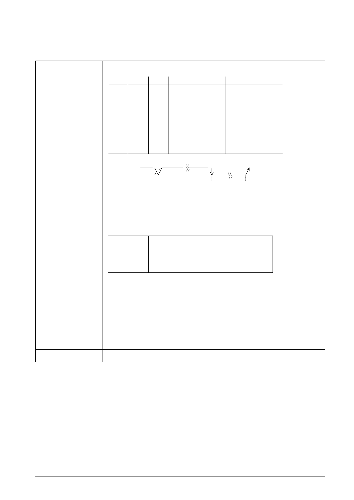
Procedures for input and output of serial data
Data is input and output using CCB (Computer Control Bus), which is SANYO’s audio IC serial bus format. This IC
adopts the 8-bit address version of the CCB format.
No. 6974-7/21
LC72148V
I/O mode
Address
Description
B0 B1 B2 B3 A0 A1 A2 A3
• Control data input (serial data input) mode
1 IN1 (84) 0 0 0 1 0 0 1 0 • 32 bits of data are input.
•
See the “Structure of the DI control data (serial data input)” item for the content of the input data.
• Control data input (serial data input) mode
2 IN2 (94) 1 0 0 1 0 0 1 0 • 32 bits of data are input.
•
See the “Structure of the DI control data (serial data input)” item for the content of the input data.
• Data output (serial data output) mode
3 OUT (A4) 0 1 0 1 0 0 1 0
• The number of bits of data output is equal to the number of clock cycles.
• See the "Structure of the DO output data (serial data output)" item for the content of the
output data.
CE
CL
DI B0 B1 B2 B3 A0 A1 A2 A3
DO
I/O mode determined
First Data IN1/2
First Data OUT
Page 8

Structure of the DI control data (serial data input)
[1] IN1 mode
[2] IN2 mode
No. 6974-8/21
LC72148V
Address
(1) P-CTR
(2) PD-C
(3) R-CTR
(4) DO-C
(5) Don’t care
(6) U-CTR
0 0 0 1 0 0 1 0
P0
P1
P2
P3
P4
P5
P6
P7
P8
P9
P10
P11
P12
P13
P14
P15
SNS
DVS
PDC0
PDC1
R0
R1
R2
R3
DT0
DT1
*
CTE
CTS0
CTS1
GT0
GT1
Address
(5) Don’t care
(5) Don’t care
(7) I/O-C
(14) TIME
(8) O-PORT
(9) U/I-C
(4) DO-C
(10) Unlock
(11) XTAL
(6) U-CTR
(12) DZ-C
(15) TEST
(13) PD-L
1 0 0 1 0 0 1 0
*
I/O-1
I/O-2
I/O-3
I/O-4
I/O-5
*
*
TBC
OUT1
OUT2
OUT3
OUT4
OUT5
OUT6
OUT7
H/I-6
L/I-7
IL0
IL1
ULD
UL0
UL1
XS
CTP
CTC
DZ0
DZ1
TEST0
TEST1
TEST2
DLC
Page 9
No. 6974-9/21
LC72148V
DI control data functions
Number
Control block/data Description Related data
• This data sets the divisor provided by the programmable divider. This is a binary value with
P15 the MSB. The LSB depends on the DVS and SNS settings.
(*: don't care)
*: When P4 is the LSB, P0 to P3 are ignored.
• DVS selects the input pin (FMIN or AMIN) whose signal is input to the programmable divider
and SNS switches the input frequency range.
*: See the “Structure of the Programmable Divider” item for details.
(1)
Programmable divider
data
P0 to P15
DVS, SNS
• Sub-charge pump control data
*: The sub-charge pump is connected to the gate of the low-pass filter amplifier transistor. A
high-speed locking circuit can be formed by using this function in conjunction with PD0 and
PD1 (main charge pump).
See the “Structure of the Charge Pump” item for details.
UL0
UL1
DLC
(2)
Sub-charge pump control
data
PDC0, PDC1
• Reference frequency selection data
*: PLL INHIBIT
In this state, the programmable divider is stopped, the FMIN and AMIN pins are pulled down to
ground, and the charge pump goes to the high-impedance state.
(3)
Reference divider data
R0 to R3
DVS SNS LSB Set divisor (N)
1 * P0 272 to 65535
0 1 P0 272 to 65535
0 0 P4 4 to 4095
R3 R2 R1 R0 Reference frequency
0 0 0 0 100 kHz
0 0 0 1 50
0 0 1 0 25
0 0 1 1 25
0 1 0 0 12.5
0 1 0 1 6.25
0 1 1 0 3.125
0 1 1 1 3.125
1 0 0 0 10
1 0 0 1 9
1 0 1 0 5
1 0 1 1 1
1 1 0 0 3
1 1 0 1 30
1 1 1 0 PLL inhibit + X’tal OSC stop
1 1 1 1 PLL inhibit
DVS SNS Input pin Input pin frequency range
1 * FMIN 10 to 180 MHz
0 1 AMIN 2 to 40 MHz
0 0 AMIN 0.5 to 10 MHz
PDC1 PDC0 Sub-charge pump state
0 * High impedance
1 1 Charge pump operation (normal)
1 0 Charge pump operation (unlocked mode)
Continued on next page.
Page 10
No. 6974-10/21
LC72148V
Continued from preceding page.
Number
Control block/data Description Related data
• This data selects the output from the DO pin.
*1. end-UC is the general-purpose counter measurement complete check function.
(1) When end-UC is set and the counter started (CTE = 0 → 1), the DO pin automatically goes to
the open state.
(2) When the general-purpose counter measurement completes, the DO pin goes to the low
level, and it becomes possible to check for the count complete state.
(3) The DO pin goes to the open state due to the I/O of serial data (when the CE pin is high).
*2
However, when the I/O-1 and I/O-2 pins are specified to be output ports, IN will go to the open
state.
*3: This is invalid if the I/O-5 pin is specified to be an input port.
Note: The DO pin will be in the open state, regardless of the state of the DO pin control data,
during the data input period (the period when CE is high in IN1 or IN2 mode).
Furthermore, the DO pin will output the content of the internal DO serial data in
synchronization with CL, regardless of the state of the DO pin control data during the data
output period (the period when CE is high in OUT mode).
DO cannot be used (it does not change state) in crystal oscillator stopped mode (R0=0,
R1=R2=R3=1).
Don’t Care
CTE
OUT5
I/O-1
I/O-2
I/O-5
(4)
DO and I/O-5 pin control
data
ULD
DT0, DT1
IL0, IL1
(5)
*
ULD DT1 DT0 DO pin state I/O-5 pin state
0 0 0 Low when the unlocked state
is detected.
0 0 1 Open OUT5 *
3
0 1 0 end-UC *
1
0 1 1 IN *
2
1 0 0 Open
1 0 1 Open Low when the unlocked state
is detected. *
3
1 1 0 end-UC *
1
1 1 1 IN *
2
IL1 IL0 IN
0 0 Open
0 1 I-1 (pin state)
1 0 I-2 (pin state)
1 1 DO goes low when I-1 changes state.
Continued on next page.
DO pin
(1) Counting starts (2) Counting completes (3) CE: HI
Page 11

No. 6974-11/21
LC72148V
Continued from preceding page.
Number
Control block/data Description Related data
• CTS1 and CTS0 select the input pin (HCTR or LCTR) for the general-purpose counter.
• CTE controls the general-purpose counter measurement operation.
CTE = 1: Starts the count
= 0: Resets the counter
• GT1 and GT0 determine the general-purpose counter measurement time (in frequency mode)
and number of periods (in period mode)
• When CTE is 0, pulling down the input is disabled by setting CTP to 1.
Note: The wait time will be 1 to 2 ms.
However, CTP must be set to 1 at least 4 ms before CTE is set to 1.
• The input sensitivity is reduced when CTC is set to 1. (Sensitivity: 10 to 30 mVrms)
* See the “Structure of the General-Purpose Counter” item for details.
H/I-6
L/I-7
(6)
General-purpose counter
control data
CTS0, CTS1
CTE
GT0, GT1
CTP
CTC
• This data specifies the I/O direction of the shared-function I/O pins (I/O-1 to I/O-5).
Data = 0: Input port
= 1: Output port
OUT1 to OUT5
ULD
(7)
I/O port control data
I/O-1 to I/O-5
• This data determines the output from the output ports O-1 to O-7.
Data= 0: Low
= 1: Open or high
• This data is invalid if input port operation or unlocked state output is specified.
I/O-1 to I/O-5
ULD
(8)
Output port data
OUT1 to OUT7
• Sets the general-purpose counter pins to function as input ports.
H/I-6 = 0: I-6 (input port)
= 1: HCTR (general-purpose counter)
L/I-3 = 0: I-7 (input port)
= 1: LCTR (general-purpose counter)
CTS0
CTS1
(9)
General-purpose counter
input control data
H/I-6, L/I-7
• UL0 and UL1 select the phase error (øE) detection width used for judging the PLL locked state.
If a phase error in excess of the widths listed in the table below occurs, the PLL will be seen to
be in the unlocked state. When unlocked, the detection pin goes low.
(* : don’t care)
ULD
DT0, DT1
(10)
Unlocked state detection
data
UL0, UL1
CTS1 CTS0 Input pin Measurement mode
1 * HCTR Frequency
0 1 LCTR Frequency
0 0 LCTR Period
UL1 UL0 øE detection width Detection output
0 0 Stopped Open
0 1 0 øE is output directly.
1 0 ±0.56 µs øE is extended by 1 to 2 ms.
1 1 ±1.11 µs øE is extended by 1 to 2 ms.
GT1 GT0
Frequency measurement
Period measurement
Measurement time Wait time
0 0 4 ms 3 to 4 ms 1 period
0 1 8 3 to 4 1 period
1 0 32 7 to 8 2 periods
1 1 64 7 to 8 2 periods
Continued on next page.
øE
DO
1 to 2 ms Extension
I/O-5
Unlocked state output
Page 12
No. 6974-12/21
LC72148V
Continued from preceding page.
Number
Control block/data Description Related data
• Selects the crystal oscillator.
XS = 1: 7.2 MHz
= 0: 4.5 MHz
* The 4.5 MHz setting is selected after the power-on reset.
(11)
Crystal oscillator circuit
XS
• Controls the phase comparator’s dead band.
The width of the dead band settings: DZA < DZB <DZC < DZD
* DZA is selected after the power-on reset. (We recommend using either DZD or DZC.) †
(12)
Phase comparator
control data
DZ0, DZ1
• This data forcibly sets the charge pump output to the low level (Vss).
DLC = 1: Low level
= 0: Normal operation
* When the circuit deadlocks due to the oscillator stopping when the PLL VCO control voltage
(Vtune) goes to 0 V, this bit can be used to clear the deadlocked state.
(Deadlock clear circuit)
This setting is set to normal operation after the power-on reset. †
(13)
Charge pump control
data
• Setting this bit to 1 causes a clock time base signal (8 Hz, 40% duty) to be output from the O-7
pin. (The OUT7 data is invalid in this mode.)
* TBC = 0 is selected after the power-on reset.
OUT7(14)
Clock time base
TBC
• IC test data.
TEST0
TEST1 All these bits must be set to 0.
TEST2
All these bits are set to 0 after the power-on reset. †
(15)
IC test data
TEST0 to TEST2
DZ1 DZ0 Dead band mode
0 0 DZA
0 1 DZB
1 0 DZC
1 1 DZD
†: Although these bits are initialized by the power-on reset circuit after power is applied, for safety, immediately after power is applied, always initialize this
setting by sending the CCB data.
Page 13
Structure of the DO output data (serial output data)
[3] OUT mode
No. 6974-13/21
LC72148V
DI 0 1 0 1 0 0 1 0
DO
I7
I6
I5
I4
I3
I2
I1
*
C19
C18
C17
C16
C15
C14
C13
C12
C11
C10C9C8C7C6C5C4C3C2C1C0**
*
*
(1) IN-PORT
(2) IF-CTR
*: Must be set to 0.
Address
Description of the DO output data
Number
Control block/data Description Related data
• This data is latched from the states of I/O port pins I-1 to I-7.
This data outputs (reports) the states of the pins regardless of the I/O direction specified for the
I/O ports. Data is latched at the point data output mode (OUT mode) is entered.
I1 to I5 ← The I/O-1 to I/O-5 pin states Hi : “1”
I6, I7 ← The HCTR/I-6 and LCTR/I-7 pin states Low : “0”
The following data is output if these pins are set to function as output ports or as generalpurpose counter input pins.
I1, I2, I3: Output pin states (open drain)
I4, I5: Output pin state (CMOS)
I6, I7: 0
I/O-1 to I/O-5
H/I-6, L/I-7
OUT1 to OUT5
(1)
I/O port data
I7 to I1
• This data is latched from the contents of the IF counter (the 20-bit binary counter).
C19 ← MSB of the binary counter
C0 ← LSB of the binary counter
CTE
CTS0
CTS1
(2)
IF counter binary data
C19 to C0
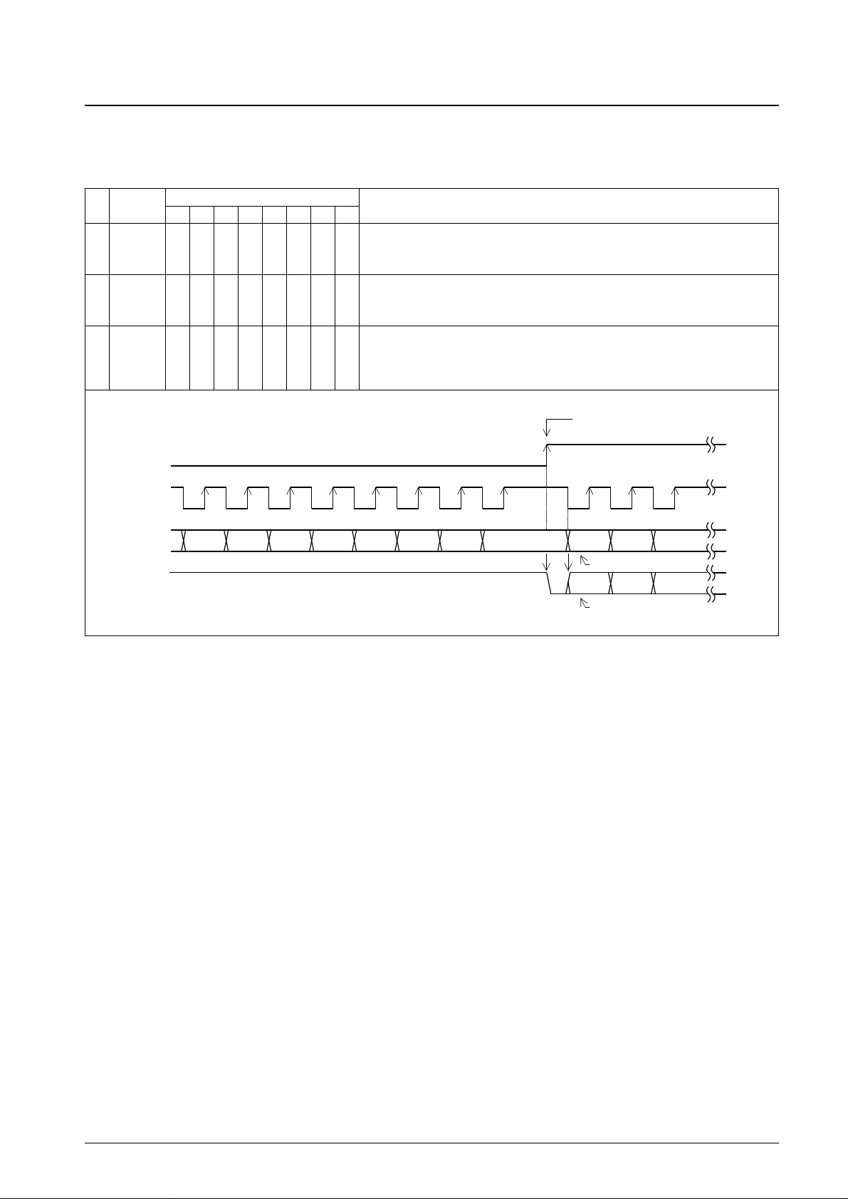
Serial data input (IN1/IN2) t
SU
, tHD, tEL, tES, tEH≥ 0.45 µs tLC< 0.45 µs
CE
CL
DI
Internal data
t
HD
t
SU
t
ES
t
EL
t
EH
t
LC
B0 B1 B2 B3 A0 A1 A2 P0 P1 P2 P3 CTS0 CTS1 GT0 GT1A3
CE
CL
DI
DO
Note: Since the DO pin is an n-channel open-drain output, the data output times (t
DC
and tDH)
depend on the value of the pull-up resistor used and the circuit board capacitance.
t
HD
t
SU
t
ES
t
EL
t
DC
t
DC
t
EH
t
DH
B0 B1 B2 B3 A0 A1 A2
I7 I6 I5 I4 C3 C2 C1 C0
A3
Serial data output (OUT) t
SU
, tHD, tEL, tES, tEH≥ 0.45 µs tDC, tDH< 0.2 µs
Page 14

No. 6974-14/21
LC72148V
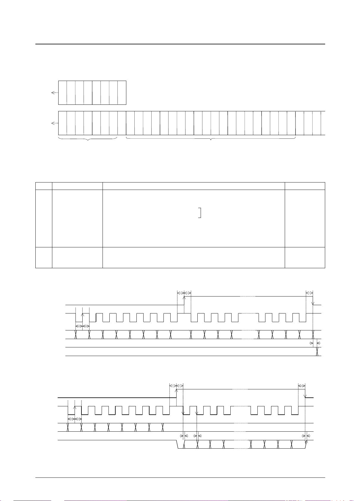
Serial data timing
CE
CL
DI
Internal data
latch
CE
CL
DI
DO
Internal data
latch
V
IH
V
IH
V
IH
V
IH
t
LC
Old New
Old New
V
IH
V
IL
V
IL
V
IL
V
IL
V
IL
t
CH
t
CL
t
EL
When stopped with CL at the low level
When stopped with CL at the high level
t
ES
t
EH
t
SU
t
HD
V
IH
V
IH
V
IH
V
IH
V
IH
V
IL
V
IL
V
IL
t
CL
t
CH
t
EL
t
ES
t
EH
t
SU
t
HD
t
DC
t
DH
t
LC
Parameter Symbol Conditions
Ratings
Unit
min typ max
Data setup time t
SU
DI, CL 0.45 µs
Data hold time t
HD
DI, CL 0.45 µs
Clock low-level time t
CL
CL 0.45 µs
Clock high-level time t
CH
CL 0.45 µs
CE wait time t
EL
CE, CL 0.45 µs
CE setup time t
ES
CE, CL 0.45 µs
CE hold time t
EH
CE, CL 0.45 µs
Data latch change time t
LC
0.45 µs
t
DC
DO, CL,
These times depend on the values of
Data output time
the pull-up resistors used and the circuit board capacitance.
0.2 µs
t
DH
DO, CE,
These times depend on the values of
the pull-up resistors used and the circuit board capacitance.
Page 15

Structure of the General-Purpose Counter
No. 6974-15/21
LC72148V
HCTR
1
2
LCTR
(FIF)
(T)
CTS1 CTS0
0–3 4–7 8–11 12–15 16–19
GT1, GT0
GT
S1
L
S
B
M
S
B
S2
S3
CTE
DO pin
One period/two period
extraction circuit
4/8/32/64 msec
Check signal: 900 kHz
Input signal
switching gate
General-purpose counter
(20-bit binary counter)
C = FIF × GT
C = (1/T) ÷ 900 kHz
CTS1 CTS0 Input pin Measurement mode Frequency range Input sensitivity
S1 1 * HCTR Frequency 0.4 to 25.0 MHz 40 mVrms *
1
S2 0 1 LCTR Frequency 10 to 500 kHz 40 mVrms *
1
S3 0 0 LCTR Period 1.0 to 20 × 103Hz (pulse)
*1 CTC = 0 : 40 mVrms
CTC = 1 : 70 mVrms
—: No rating (not guaranteed)
( ): Actual performance (provided for reference purposes)
CTC is the input sensitivity switching data; when CTC is 1, the input sensitivity is degraded.
However, the actual performance will be:
HCTR → 20 to 40 mV rms (frequency: 10.7 MHz)
LCTR → 20 to 30 mV rms (frequency: 450 kHz)
CTP: Pulling down the input is disabled (when CTE is 0) by setting CTP to 1.
CTP must be set to 1 at least 4 ms before CTE is set to 1. If the counter is not used, CTP must be left set to 0. The wait
time is reduced 1 to 2 ms when CTP is set to 1.
HCTR: Minimum input sensitivity rating f [MHz]
CTC 0.4 ≤ f < 8 8 ≤ f < 12 12 ≤ f ≤ 25
0 (Normal mode) 40 mVrms
40 mVrms
40 mVrms
(0.1 to 5 mVrms)
1 (Degraded mode) —
70 mVrms
—
(20 to 40 mVrms)
LCTR: Minimum input sensitivity rating f [kHz]
CTC 10 ≤ f < 400 400 ≤ f ≤ 500
0 (Normal mode) 40 mVrms
20 mVrms
(0.1 to 4 mVrms)
1 (Degraded mode) —
70 mVrms
(20 to 30 mVrms)
GT1 GT0
Frequency measurement mode Period measurement
Measurement time Wait time mode
0 0 4 ms
3 to 4 ms 1 period
0 1 8
1 0 32
7 to 8 ms 2 periods
1 1 64
Page 16
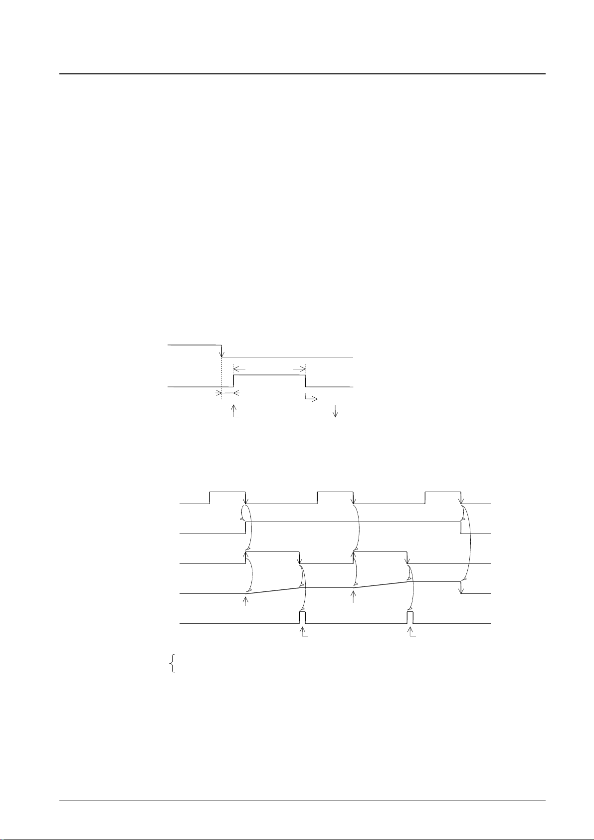
The LC72148V general-purpose counter is a 20-bit binary counter. The results of count operations can be read out MSB
first through the DO pin. When using the general-purpose counter for frequency measurement, one of four times, 4, 8, 32,
or 64 ms, can be selected as the measurement time with GT0 and GT1. The frequency of the signal input to either the
HCTR or LCTR pin can be measured by determining how many pulses were input to the general-purpose counter during
this measurement time.
When using the general-purpose counter for frequency measurement, the period of the signal input to the LCTR pin can
be measured by determining how many cycles of the check signal (900 kHz) were input to the general-purpose counter
during 1 or 2 periods of the signal input to the LCTR pin.
The general-purpose counter counting is started by setting CTE in the serial data to 1. The serial data is confirmed
internally to the LC72148V by dropping the CE signal from high to low. However, the signal input to the HCTR or
LCTR pin must be provided within the wait time after CE is set low.
Next, the value of the general-purpose counter following completion of the measurement must be read out during the
period while CTE is 1. (The general-purpose counter is reset when CTE is set to 0.)
One point that requires care here is that the general-purpose counter must be reset (cleared) by setting CTE to 0 before
starting the general-purpose counter. Another is that although the signal input to the LCTR pin is transmitted directly to
the general-purpose counter, the signal input to the HCTR pin is passed through a divide-by-two circuit before being
transmitted to the general-purpose counter. Therefore, the result of the count by the general-purpose counter for the
HCTR pin is 1/2 the value as compared to the actual frequency input to the HCTR pin.
No. 6974-16/21
LC72148V
CE
CE
Internal data
latch (CTE)
GT
General-purpose
counter
end-UC
CTE = 1
Measurement
time
end-UC
t
WU
: Wait time
t
WU
End
GT
Count start
Start
Restart
Count end Count end
Reset
CTE = 1 CTE = 1 CTE = 0
(Integration)
*: CTE: 0 →
1 →
• Resets the general-purpose counter
• Starts the general-purpose counter
• Restarts when set to 1 again.
For an integrating count, the value counted is accumulated in the general-purpose counter.
Here, counter overflow may occur, and requires caution.
Count value: 0
H
to FFFFFH (1,048,575)
For an integrating count
Page 17

Structure of the Charge Pump
No. 6974-17/21
LC72148V
DLC
Phase
Detector
Unlock
Detector
and
Subcharge
Pump Cont
Unlock
(Main)
(Main)
PDS
R1S
(SUB)
DO or I/O-5 pins
DZ1DZ0
PDC1PDC0
Clock
UL0
UL1
fvco/N
fref
PD1
PD0
AIN
AOUT
Vssa
R1S = 300 Ω (typ)
PD0
PDS
R1S
R1M
Vcc
Vtune
PDC1 PDC0 PDS (Sub-charge pump state)
0 * High impedance
1 1 Charge pump operation (normal)
1 0 Charge pump operation (unlocked mode)
DLC PD1, PD0, PDS
0 Normal operation
1 Forced low.
Note*: When the unlocked state is detected when changing stations, PDS (the sub-charge pump) operates, R1 becomes R1M/R1S, the low-pass filter time
constant is made smaller, and frequency locking is accelerated.
Page 18

Other Items
1. Notes on the phase comparator dead band
When the charge pumps are in one of the ON/ON states, correction pulses will be output from the charge pumps even
if the PLL is locked, making it easier for the loop to become unstable. Thus particular care is required in the design
stage for these settings.
The following problems may occur when the ON/ON states are used.
(1) Side bands may be created by reference frequency leakage.
(2) Side bands may be created by low-frequency leakage due to the envelope of the correction pulses.
When a dead band is present (the OFF/OFF settings), the loop will be stable. However, it will be difficult to achieve a
high signal-to-noise ratio. Inversely, with no dead band, it is easy to achieve a high signal-to-noise ratio but hard to
achieve high loop stability.
Therefore, the DZA and DZB settings, in which there is no dead band, can be effective for cases where an FM signalto-noise ratio of 90 to 100 dB or greater is required, or when it is desirable to increase the AM stereo pilot margin.
However, if such a high signal-to-noise ratio is not required in FM reception, or an adequate AM stereo pilot margin
can be achieved, or AM stereo is not used, DZC or DZD, which provide a dead band, should be selected.
Dead Zone (Dead Band) Definition
The phase comparator compares fp with the reference frequency (fr) as shown in figure 1. This circuit outputs a level
(A) that is proportional to the phase difference ø as shown in figure 2. However, due to internal delays and other
factors, the actual IC is unable to compare small phase differences, and thus a dead zone (B) appears in the output. To
achieve a high signal-to-noise ratio in the end product, the dead zone should be as small as possible.
However, in popularly-priced models, there are cases where a somewhat wider dead zone may be easier to work with.
This is because in some situations, such as when a powerful signal is applied to the RF input, in popularly-priced
models there may be RF leakage from the mixer to the VCO. When the dead zone is narrow, outputs to correct this
leakage are output, that output in turn modulates the VCO, and generates a beat signal with the RF.
2. Notes on the FMIN, AMIN, HCTR/I-6, and LCTR/I-7 pins
The coupling capacitors must be located as close as possible to these pins. A capacitance of approximately 100 pF is
desirable.
In particular, if the HCTR/I-6 and LCTR/I-7 pin capacitors are over about 1000 pF, the time required to reach the bias
level may become excessive, and incorrect counting may occur due to the relationship with the wait time.
No. 6974-18/21
LC72148V
DZ1 DZ0 Dead band mode Charge pumps Dead band
0 0 DZA ON/ON - - 0 s
0 1 DZB ON/ON - 0 s
1 0 DZC OFF/OFF +0 s
1 1 DZD OFF/OFF ++0 s
Figure 1 Figure 2
V
(A)
(B)
ø (ns)
Dead Zone
Reference divider
Programmable divider
RF
MIX
fr
Phase
Detector
fp
Leakage
LPF VCO
Page 19

No. 6974-19/21
LC72148V
3. Notes on using IF counting with the HCTR/I-6 and LCTR/I-7 pins
If IF counting is used, the microcontroller must test the state of the IF IC SD (station detect) signal, and only if the SD
signal is present, turn on the IF counter buffer output and perform an IF count operation. Methods in which autosearch operations are implemented only using the IF count may incorrectly stop at frequencies where no station is
present due to leakage from the IF counter buffer.
4. Using the DO pin
At times other than data output mode, the DO pin can also be used to check for general-purpose counter count
operation completion, to output the unlock state detection signal, and to check for changes in the input pins.
Note that the states of the input pins (I/O-1 and I/O-2) can be input to the system microcontroller through the DO pin.
5. Power supply pins
Capacitors must be inserted between the VDDand V
SSd
power supply pins to reduce noise. These capacitors must be
located as close to the VDDand V
SSd
pins as possible.
6. Notes on VCO design
The VCO (local oscillator) must be designed so that the VCO oscillation does not stop if the control voltage (Vtune)
becomes 0 V. If it is possible for this oscillator to stop, use the charge pump control data (DLC) to forcible set Vtune
to VCCtemporarily to prevent the PLL circuit from deadlocking. (This function is called a deadlock clear circuit.)
7. Notes on the PD pin
When switching from the LC72146 (5 V system) to this IC (3 V system), the charge pump output voltage will be
reduced, thus reducing the loop gain. Thus various aspects of the circuit, such as the loop filter coefficients, and the
locking time (the SD wait time) must be reviewed.
8. Microcontroller interface
Although this IC is a 3 V system IC, it can accept 5 V system inputs over the microcontroller interface (the CE, DI,
and CL pins).
Pin states after a power-on reset
O: Open, L: Low, F: Floating
State Power-on reset
O O-7
L O-6
F I-5
F I-4
F I-3
F I-2
F I-1
StatePower-on reset
FI-6
FI-7
XOUT
CE
DI
CL
DO
O-7
O-6
I/O-5
I/O-4
I/O-3
I/O-2
I/O-1
XIN
V
SSa
AOUT
AIN
PD0
PD1
V
SSd
FMIN
AMIN
VDD
HCTR/I-6
LCTR/I-7
LC72148V
Page 20

Sample Application Circuit
No. 6974-20/21
LC72148V
Microcontroller
SO DI
CL
DO
SI
end-UC
Unlock
ST/MON
SD
CE
XOUT 1
CE 2
DI 3
CL 4
DO 5
O-7 6
O-6 7
I/O-5 8
I/O-4 9
I/O-3 10
I/O-2 11
I/O-1
XIN
VSSa
AOUT
AIN
PD0
PD1
VSSd
FMIN
AMIN
VDD
HCTR/I-6
LCTR/I-712
24
23
22
21
20
19
18
17
16
15
14
13
FMVcc
FMVCO
AMVCO
AMVcc
IF FMVcc
ST/MON
SD
STRQ
IF AMVcc
ST/MON
SD
STRQ
Page 21

PS No. 6974-21/21
LC72148V
This catalog provides information as of April, 2002. Specificati ons and information herein are
subject to change without notice.
Specifications of any and all SANYO products described or contained herein stipulate the performance,
characteristics, and functions of the described products in the independent state, and are not guarantees
of the performance, characteristics, and functions of the described products as mounted in the customer’s
products or equipment. To verify symptoms and states that cannot be evaluated in an independent device,
the customer should always evaluate and test devices mounted in the customer’s products or equipment.
SANYO Electric Co., Ltd. strives to supply high-quality high-reliability products. However, any and all
semiconductor products fail with some probability. It is possible that these probabilistic failures could
give rise to accidents or events that could endanger human lives, that could give rise to smoke or fire,
or that could cause damage to other property. When designing equipment, adopt safety measures so
that these kinds of accidents or events cannot occur. Such measures include but are not limited to protective
circuits and error prevention circuits for safe design, redundant design, and structural design.
In the event that any or all SANYO products (including technical data, services) described or contained
herein are controlled under any of applicable local export control laws and regulations, such products must
not be exported without obtaining the export license from the authorities concerned in accordance with the
above law.
No part of this publication may be reproduced or transmitted in any form or by any means, electronic or
mechanical, including photocopying and recording, or any information storage or retrieval system,
or otherwise, without the prior written permission of SANYO Electric Co., Ltd.
Any and all information described or contained herein are subject to change without notice due to
product/technology improvement, etc. When designing equipment, refer to the “Delivery Specification”
for the SANYO product that you intend to use.
Information (including circuit diagrams and circuit parameters) herein is for example only; it is not
guaranteed for volume production. SANYO believes information herein is accurate and reliable, but
no guarantees are made or implied regarding its use or any infringements of intellectual property rights
or other rights of third parties.
 Loading...