

Page 1
Any and all SANYO products described or contained herein do not have specifications that can handle
applications that require extremely high levels of reliability, such as life-support systems, aircraft’s
control systems, or other applications whose failure can be reasonably expected to result in serious
physical and/or material damage. Consult with your SANYO representative nearest you before using
any SANYO products described or contained herein in such applications.
SANYO assumes no responsibility for equipment failures that result from using products at values that
exceed, even momentarily, rated values (such as maximum ratings, operating condition ranges,or other
parameters) listed in products specifications of any and all SANYO products described or contained
herein.
CMOS IC
PLL Frequency Synthesizers
Ordering number:ENN4464A
LC72140, 72140M
SANYO Electric Co.,Ltd. Semiconductor Company
TOKYO OFFICE Tokyo Bldg., 1-10, 1 Chome, Ueno, Taito-ku, TOKYO, 110-8534 JAPAN
Overview
The LC72140 and LC72140M are high-performance,
phase-locked loop (PLL) frequency synthesizers that operate over the VHF, MW and LW wave bands. They feature
excellent frequency tracking, making them ideal as a reference frequency source for use in AM/FM radio receivers.
The LC72140 and LC72140M operate from a 5V supply.
The LC72140 is available in 24-pin DIPs, and the
LC72140M, in 24-pin MFPs.
Features
• High-speed programmable dividers for
· 10 to 160MHz on FMIN using pulse swallower.
· 0.5 to 40.0MHz on AMIN using pulse swallower and
direct division.
• General-purpose counters (used together with the SD in
IF count mode).
· HCTR for 0.4 to 25.0MHz frequency measurement.
· LCTR for 10 to 500kHz frequency measurement and
1Hz to 20kHz period measurement.
• 4.5 or 7.2MHz crystal.
• Twelve selectable reference frequencies (1, 3, 5, 9, 10,
3.125, 6.25, 12.5, 25, 30, 50 and 100kHz).
• Phase comparator.
· Insensitive band control.
· Unlock detection.
· Sub-charge pump for high-speed locking.
· Deadlock clear circuit.
• C2B input/output data interface.
• Power-ON reset circuit.
• Built-in MOS transistor for a low-pass filter.
• Inputs/outputs (using five general-purpose input/output
ports).
· Maximum of seven inputs.
· Maximum of seven outputs (three n-channel open-drain
and four CMOS outputs).
• 5V supply.
• 24-pin DIP (LC72140) and 24-pin MFP (LC72140M).
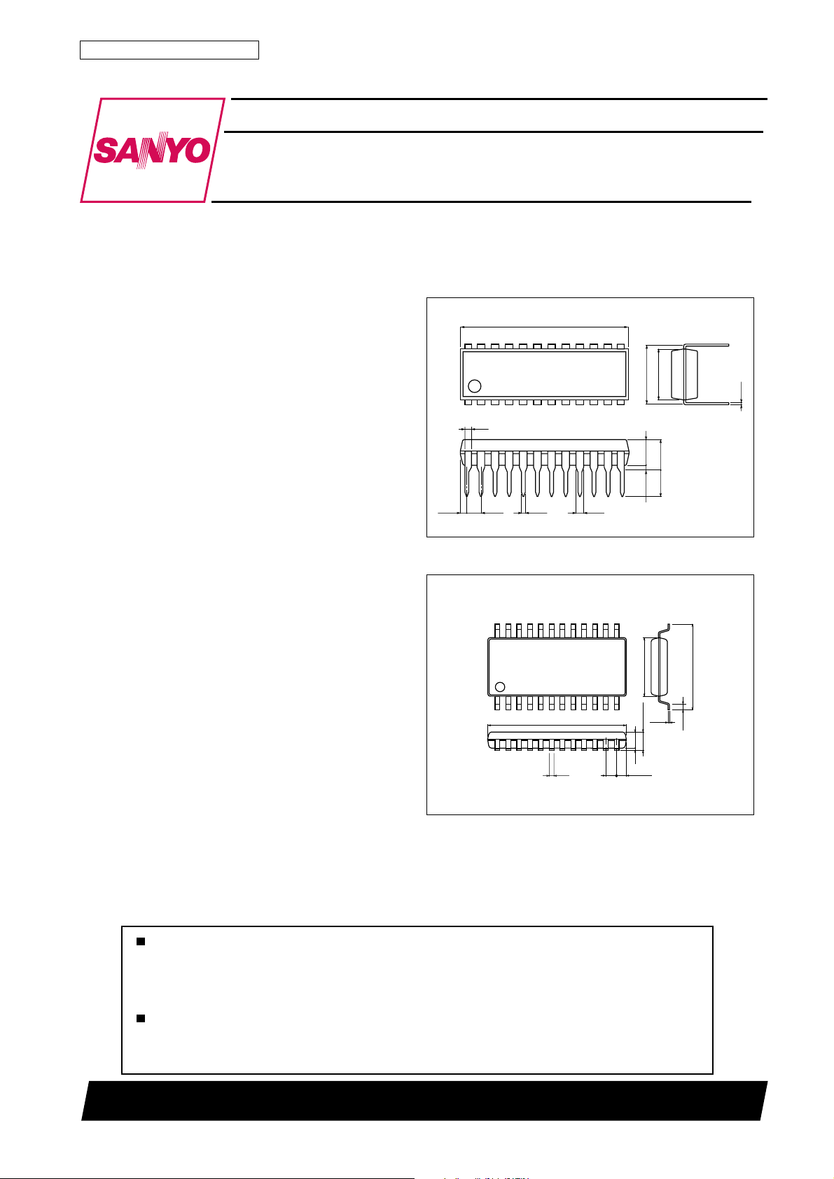
Package Dimensions
unit:mm
3067A-DIP24S
[LC72140]
21.0
24
1
0.9
(0.71)
1.78
unit:mm
3112A-MFP24S
0.48
24
112
0.95
[LC72140M]
12.5
0.35
13
6.4
7.62
0.25
12
(3.25)
3.9max
3.3
0.51min
SANYO : DIP24S
13
5.4
1.7max
1.5
0.1
1.0
(0.75)
7.6
0.15
0.63
SANYO : MFP24S
71901TN (KT)/50195TH (ID)/80593JN No.4464–1/15
Page 2
Pin Assignment
Block Diagram
LC72140, 72140M
No.4464–2/15
Page 3
Pin Functions
rebmuNemaNtiucrictnelaviuqEnoitcnuF
1TUOX tuptuorotallicsolatsyrczHM2.7ot5.4
42NIX tupnirotallicsolatsyrczHM2.7ro5.4
2ECtupnielbane-pihC
3IDrellortnocorcimmorftupniataD
4LCtupnikcolC
5ODrellortnocorcimottuptuoataD
LC72140, 72140M
67Otuptuogalf7TUO
76Otuptuogalf6TUO
85O/I
94O/I
013O/I
21O/I
5dna4stroptuptuo/tupniesoprup-lareneG
3ot1stroptuptuo/tupniesoprup-lareneG112O/I
317I/RTCL
.7
troptupnidnatupniretnuocesoprup-larenegtnemerusaemycneuqerfrodoireP
Continued on next page.
No.4464–3/15
Page 4
Continued from preceding page.
rebmuNemaNtiucrictnelaviuqEnoitcnuF
416I/RTCH .6troptupnidnatupniretnuocesoprup-larenegtnemerusaemycneuqerF
LC72140, 72140M
51V
61NIMA tupnilangisrotallicsolacoldnabMA
71NIMF tupnilangisrotallicsolacoldnabMF
911DP
020DP
12NIA tupnirotsisnartretlifssap-wolgolanA
DD
egatlovylppuS
stuptuopmupegrahcrotceted-esahP
22TUOA tupuorotsisnartretlifssap-wolgolanA
32,81V
SS
Specifications
Absolute Maximum Ratings at Ta = 25˚C, VSS=0V
retemaraPlobmySsnoitidnoCsgnitaRtinU
egatlovylppusmumixaMV
egatlovtupniIDdnaLC,ECmumixaMV
egatlovtupni3O/Iot1O/ImumixaMV
sniprehtollarofegatlovtupnimumixaMV
egatlovtuptuoODmumixaMV
egatlov
tnerruc
noitapissidrewopelbawollAxamdP
erutarepmetgnitarepOrpoT 58+ot04–
erutarepmetegarotSgtsT 521+ot55–
tuptuoTUOAdna3O/Iot1O/ImumixaM
sniprehtollarofegatlovtuptuomumixaMV
V
tnerructuptuo7Odna6O,5O/I,4O/ImumixaMI
tuptuoTUOAdnaOD,3O/Iot1O/ImumixaM
xam 0.7+ot3.0–V
DD
xam 0.7+ot3.0–V
1NI
xam 0.51+ot3.0–V
2NI
xam Vot3.0–
3NI
xam 0.7+ot3.0–V
1TUO
xam 0.51+ot3.0–V
2TUO
xam Vot3.0–
3TUO
xam 0.3ot0Am
1TUO
I
xam 0.6ot0Am
2TUO
DIP24S, T a≤85˚C
MFP24S, T a≤85˚C
dnuorG
3.0+V
DD
3.0+V
DD
053Wm
061Wm
˚C
˚C
No.4464–4/15
Page 5

LC72140, 72140M
Allowable Operating Ranges at Ta = –40 to +85˚C, VSS=0V
retemaraPlobmySsnoitidnoC
egatlovylppuS
egatlov
egatlovtupni
egatlovtupnilevel-wol
egatlovtupnilevel-hgih7I/RTCLV
egatlovtupnilevel-wol7I/RTCLV
egatlovtuptuoODV
ycneuqerftupniNIXf
ycneuqerftupniNIMFf
ycneuqerftupniNIMAf
ycneuqerftupni6I/RTCHf
ycneuqerftupni7I/RTCLf
ycneuqerfrotallicsolatsyrCf
edutilpmatupnismrNIXV
edutilpmatupnismrNIMFV
edutilpmatupnismrNIMAV
edutilpmatupnismr6I/RTCHV
edutilpmatupnismr7I/RTCHV
emitputesatadLCotIDt
emitdlohatadLCotIDt
htdiweslupkcolclevel-wolLCt
htdiweslupkcolclevel-hgihLCt
emittiawelbanepihcECotLCt
emitputeselbanepihcLCotECt
emitdlohelbanepihcECotLCt
emithctalatadotelbanepihCt
emittuptuoatadODotLCt
emittuptuoatadODotECt
tupnilevel-hgih3O/Iot1O/IdnaID,LC,EC
level-hgih7I/RTCLdna6I/RTCH,5O/I,4O/I
egatlovtuptuoTUOAdna3O/Iot1O/IV
V
V
V
V
7I/RTCLdna6I/RTCH,5O/Iot1O/I,ID,EC,LC
V
V
1DD
V
2DD
1HI
2HI
1LI
3HI
2LI
1TUO
2TUO
1NI
2NI
3NI
4NI
5NI
LATX
1NI
05 ≤ rediviDelbammargorPeeS.zHM031<f
2NI
01 ≤ 031dna05<f ≤f≤ eeS.zHM061
2≤ rediviDelbammargorPeeS.zHM52<f
52 ≤f≤ rediviDelbammargorPeeS.zHM04
3NI
4NI
5NI
US
DH
LC
HC
LE
SE
HE
CL
CD
HD
DD
DD
5.0 ≤ rediviDelbammargorPeeS.zHM5.2<f
5.2 ≤f≤ rediviDelbammargorPeeS.zHM01
.noitces
.noitces
.noitces
.noitces
.noitces
sgnitaR
nimpytxam
5.45.5V
egatlovniatsusatadlaires:0.2V
2.25.6V
2.2V
08.0V
tnemerusaemdoirep,evawesluP2.2V
tnemerusaemdoirep,evawesluP08.0V
05.6V
031V
gnilpuoceviticapac,evaweniS0.10.8zHM
gnilpuoceviticapac,evaweniS01061zHM
gnilpuoceviticapac,evaweniS5.00.04zHM
gnilpuoceviticapac,evaweniS4.052zHM
gnilpuoceviticapac,evaweniS01005zHk
gnilpuocCD,evaweslup,tnemerusaemdoireP100.00.02zHk
ecnadepmilatsyrC ≤ 021 Ω 0.40.8zHM
2.05.1V
70.05.1V
.noitcesrediviDelbammargorP
rotsiserpu-llupnosdnepeD 2.0sµ
01.05.1V
40.05.1V
70.05.1V
40.05.1V
70.05.1V
40.05.1V
40.05.1V
54.0sµ
54.0sµ
54.0sµ
54.0sµ
54.0sµ
54.0sµ
54.0sµ
DD
DD
54.0sµ
tinU
V
V
Electrical Characteristics at Ta = –40 to +85˚C, VSS=0V
retemaraPlobmySsnoitidnoC
ecnatsiserlanretniNIXR
ecnatsiserlanretniNIMFR
ecnatsiserlanretniNIMAR
ecnatsiserlanretni6I/RTCHR
ecnatsiserlanretni7I/RTCLR
ecnatsiserlanretnipmupegrahc-busNIAS1R 005
htdiwsiseretsyh7I/RTCLdnaID,LC,ECV
egatlovtuptuo
egatlovtuptuolevel-hgihNIAV
egatlovtuptuo
egatlovtuptuolevel-wolTUOAV
egatlovtuptuolevel-wolNIAV
level-hgih7Odna6O,5O/I,4O/I,1DP,0DP
level-wol7Odna6O,5O/I,4O/I,1DP,0DP
egatlovtuptuolevel-wolODdna3O/Iot1O/IV
1f
2f
3f
4f
5f
H
V
V
IOAm1=
1HO
IOAm1=
2HO
IOAm1= 0.1V
1LO
IOAm5= 0.1V
2LO
I
3LO
4LO
V,Am1=
O
IOAm1=7.05.1V
sgnitaR
nimpytxam
0.1MΩ
005kΩ
005kΩ
005kΩ
005kΩ
V1.0
DD
VDD0.1–
VDD5.1–VDD7.0–
V3.1=5.0V
NIA
Continued on next page.
No.4464–5/15
tinU
Ω
V
V
V
Page 6

LC72140, 72140M
Continued from preceding page.
retemaraPlobmySsnoitidnoC
tnerructupnilevel-hgihIDdnaLC,ECI
tnerructupnilevel-hgih3O/Iot1O/II
tnerructupni
tnerructupnilevel-hgihNIXI
tnerructupni
tnerructupnilevel-wolNIXI
tnerructupni
tnerrucegakaeltuptuoODI
tnerruc
tnerruc
tnerrucylppuSI
ecnaticapactupniNIMFC
level-hgih7I/RTCLdna6I/RTCH,5O/I,4O/I
tnerructupnilevel-wolIDdnaLC,ECI
tnerructupnilevel-wol5O/Iot1O/II
tnerructupnilevel-wol7I/RTCLdna6I/RTCHI
egakaellevel-woletatsirtNIAdna1DP,0DP
egakaellevel-hgihetatsirtNIAdna1DP,0DP
I
level-hgih7I/RTCLdna6I/RTCH,NIMA,NIMF
I
level-wol7I/RTCLdna6I/RTCH,NIMA,NIMF
I
tnerrucegakaeltuptuoTUOAdna3O/Iot1O/II
I
I
V
1HI
2HI
3HI
4HI
5HI
1LI
2LI
3LI
4LI
5LI
1FFO
2FFO
LFFO
HFFO
DD
NI
V5.6= 0.5Aµ
NI
VNIV31= 0.5Aµ
VNIV=
DD
VNIV=
DD
VNIV=
DD
VNIV0= 0.5Aµ
VNIV0= 0.5Aµ
VNIV0= 0.5Aµ
VNIV0=5.311Aµ
VNIV0=0.681Aµ
VOV31= 0.5Aµ
VOV5.6= 0.5Aµ
VOV0=10.0002An
VOV=
DD
f
2NI
f
4NI
f
LATX
V,zHM061=
2NI
V,zHM52=
zHM2.7=
Vm04=
4NI
f,Vm001=
LATX
,gninnurrotallicsolatsyrc,detibihniLLP
deppotsrotallicsolatsyrc,detibihniLLP 01Aµ
nimpytxam
5.311Aµ
0.681Aµ
,zHM2.7=
Functional Description
Serial Data Input
The LC72140 and LC72140M operating parameters are initialized by two 40-bit data words on the serial data input, DI,
as shown in Figures 1 and 2 and Table 1.
sgnitaR
0.5Aµ
10.0002An
0151Am
5.0Am
6Fp
tinU
Figure 1. Input data word IN1
Figure 2. Input data word IN2
No.4464–6/15
Page 7

Table 1. Input data functions
emaNnoitcnuFstibdetaleR
,51Pot0P
SVD,SNS
1CDP,0CDP
3Rot0R
etoN
× eract'nod=
etoN
× eract'nod=
etoN
× eract'nod=
LC72140, 72140M
oitarredividelbammargorP
sgnittesoitarrediviD.2elbaT
SVDSNSbsIoitarrediviD
1
01 0P53556ot272
00 4P5904ot4
SVDSNStroptupnIegnarycneuqerftupnI
1
01 NIMAzHM04ot2
00 NIMAzHM01ot5.0
0
11 )ylsuounitnocsetarepo(gnitarepO
10 )dekcolnusiLLPnehw(gnitarepO
3R2RR1R
0000 001
0001 05
0010 52
0011 52
0100 5.21
0101 52.6
0110 521.3
0111 521.3
1000 01
1001 9
1010 5
1011 1
1100 3
1101 03
1110 deppotsrotallicsolatsyrcdnadetibihniLLP
1111 detibihniLLP
×
0P53556ot272
sgnittesegnarycneuqerF.3elbaT
×
lortnocpmupegrahC
NIMFzHM061ot01
noitcelesetatspmupegrahC.4elbaT
0CDP1CDPetatspmupegrahC
×
tcelesycneuqerfecnerefeR
noitcelesycneuqerfecnerefeR.5elbaT
0
.LLPgnikcoltsafadliubot)pmupegrahcniam(1DPdna
ecnadepmi-hgiH
ehtfognittesehtybdenimretederabsldnaegnarycneuqerf,oitarredividehT.bsmehtsi51P
.bsIehtsi4Pfiderongiera3Pot0P.3dna2selbaTninwohssasgalfSNSdnaSVD
pmupegnahc-busehT.4elbaTninwohssaetatspmupegrahcehtlortnoc1CDPdna0CDPstiB
0DPhtiwnoitcnujnocnidesuebnacsihT.rotsisnartretlifssapwolehtfoetagehtotdetcennocsi
CLD,1LU,0LU
.5elbaTninwohssaycneuqerfecnereferehttcelesroLLPehtelbasid3Rot0RstiB
)zHk(ycneuqerfecnerefeR
otdelluperaNIMFdnaNIMA,deppotssiredividelbammargorpeht,delbasidsiLLPehtnehW
.ecnadepmihgihemocebstuptuopmup-egrahcehtdna,dnuorg
Continued on next page.
No.4464–7/15
Page 8

Continued from preceding page.
emaNnoitcnuFstibdetaleR
,1TD,0TD,DLU
1LI,0LI
× eract'nod=
,ETC,1STC,0STC
1TG,0TG
5O/Iot1O/I
7TUOot1TUO
7I/L,6I/H
LC72140, 72140M
atadlortnoctuptuo5O/IdnaOD
.7dna
noitcelesgalftuptuo5O/IdnaOD.6elbaT
DLU1TD0TDOD5O/I
000 galfkcolnU
001 nepO
010 .1etoneeS.galfCU-dnE
011 .7elbateeS.NI
100 nepO
101 nepO
110 galfCU-dnE
111 .7elbateeS.NI
setoN
.troptuptuonaebottessi5O/IfiylnoelbacilppA.2
etatstuptuoOD.3erugiF
noitcelesetatsNI.7elbaT
1LI0LIetatsNI
00nepO
01tupni1I
10tupni2I
11 .segnahc1InehwWOLseogOD
setoN
lortnocretnuoC
hctiwS1STC0STCtupnI
1S1
2S01 RTCLycneuqerFzHk005ot01Vm04
3S00 RTCLdoirePzHk02otzH1)esluP(
etoN
×
RTCHycneuqerFzHM0.52ot4.0Vm04
edom
noitcelesnoitarudtnemerusaeM.9elbaT
1TG0TG
00 4
01 8
10 23
11 46
lortnoctroptuptuo/tupnI
atadtroptuptuO
lortnoctupniretnuoC
noitarudtnemerusaeM
)sm(
.neposemocebNI,troptuptuonaebottessi2O/Iro1O/IfI.1
.deppotssahrotallicsolatsyrcehtnehwWOLogtonseodOD.2
noitcelesedomtnemerusaemdnatupniretnuoC.8elbaT
tnemerusaeM
tnemerusaemycneuqerFtnemerusaemdoireP
)sm(emittiaWselcyC
4ot31
8ot72
.tuptuokcolnuehtrotroptupninasitropgnidnopserroc
.tupniRTCLehtsi7I/RTCL,1si7I/Lnehwdna,troptupni
6selbaTninwohssa5O/IdnaODstuptuofoedomehtlortnoc1LIdna0LI,1TD,0TD,DLUstiB
.2etoNeeS.galf5TUO
.2etoNeeS.galfkcolnU
.dehsinifsahnoitareporetnuocesoprup-larenegtahtsgalfCU-dnE.1
.8elbaTninwohssatupniretnuocehttceles1STCdna0STCstiB
ycneuqerF
egnar
.0nehw,retnuocehtsteserdna,1nehwretnuocehtstratsETCtiB
.9lebaTninwohssaedomtnemerusaemdoirepnitnuocotsdoirepfo
smrtupnI
ytivitisnes
rebmunehtroedomtnemerusaemycneuqerfniemittnemerusaemehttceles1TGdna0TGstiB
sitibgnidnopserrocehtnehwtupninasiniphcaE.stropehtfonoitceridehttes5O/Iot1O/IstiB
.teserNO-rewopretfastupniebotteserastropllA.1sitibehtnehw,tuptuonadna,0
roneposituptuohcaE.stroptuptuo7Oot1Oehtfoseulavtuptuoehttes7TUOot1TUOstiB
ehtfiderongisitibA.0sitibehtnehw,WOLdna,1sitibgnidnopserrocehtnehwHGIH
6I/RTCH,0si6I/HnehW.snip7I/RTCLdna6I/RTCHehtfonoitarepoehttceles7I/Ldna6I/HstiB
nasi7I/RTCL,0si7I/LnehW.tupniRTCHehtsi6I/RTCH,1si6I/Hnehwdna,troptupninasi
,1O/I,5TUO
5O/I,2O/I
7I/L,6I/H
,5TUOot1TUO
DLU
DLU,5O/Iot1O/I
1STC,0STC
Continued on next page.
No.4464–8/15
Page 9

Continued from preceding page.
emaNnoitcnuFstibdetaleR
1LU,0LU
SX
1ZD,0ZD
CLD
2TSETot0TSET
LC72140, 72140M
lortnoctcetedkcolnuLLP
1LU0LUrorreesahPtuptuorotceteD
00 deppotSnepO
01 0
10 sµ65.0±
11 sµ11.1±
lortnocrotallicsolatsyrC
.zHM5.4
lortnocrotarapmocesahP
1ZD0ZDedom)enozdaed(dnabevitisnesnI
00 AZD
01 BZD
10 CZD
11 DZD
lortnocpmupegrahC
VegatlovlortnocOCV
enut
.OCVehtgnitratser
atadtseT
.teserNO-rewoparetfa
.teserNO-rewopretfadetcelessizHM5.4
noitcelesedomdnabevitisnesnI.11elbaT
.teserNO-rewopretfadetcelessiAZD
(noisnetxednadlohserhtrorreesahpehttceles1LU0LUstiB φ
E
.WOLseogtuptuorotcetedkcolnuLLPeht,rorredetceles
LLPehttcetedotdesu)
ehtnahtretaergsirorreesahpehtnehW.4erugiFdna01elbaTninwohssaetatsdekcolnu
noitcelesnoisnetxednanoitcetedkcolnU.01elbaT
φ
tuptuo
E
φ
E
φ
E
noisnetxerorre-esahP.4erugiF
.yllamronsetarepopmupegrahceht,0siCLDnehwdna,WOLot
.teserNO-rewopretfadetcelessiedomgnitarepoyllamroN
noisnetxesm2ot1htiw
noisnetxesm2ot1htiw
,0siSXnehwdna,zHM2.7siycneuqerfeht,1siSXnehW.ycneuqerfrotallicsoehtstcelesSXtiB
.enozdaedro,dnabevitisnesnirotarapmocesahpehttceles1ZDdna0ZDstiB
decroferastuptuopmupegrahceht,1siCLDnehW.noitarepopmupegrahcehtslortnocCLDtiB
Vstes1otCLDgnitteS.OCVehtgnitlah,V0semoceb
enut
stifikcoldaednacLLPehT.etatskcoldaedamorfLLPehtevomerotlufesuebnacerutaefsihT
Vot
,
CC
orezotteserayehT.0otllamehtteS.gnitsetecivedyrotcaf-nirofdesuera2TSETot0TSETstiB
1TD,0TD,DLU
Serial Data Input Timing
The timing for the serial data input words is shown in Figure 5. The first eight bits are the mode select bits.
Figure 5. Input timing
Notes
1. tSU, tHD, tEL, tES, tCL, tCH and tEH>0.45µs
2. tLC<0.45µs
No.4464–9/15
Page 10

LC72140, 72140M
Serial Data Output
The 40-bit data word output on DO has the format and functions as shown in Figure 6 and Table 12, respectively.
Figure 6. Output data word OUT
Table 12. Input data functions
emaNnoitcnuFstibdetaleR
atadtroptupnI
7Iot1I
91Cot0C
stnetnocretnuoC
.bsIehtsi0C.retnuocyranibtib-02ehtfostnetnocdehctalehtera91Cot0CstiB
tuptuoatadotsegnahcecivedehtnehwtroptupnihcaeotnidehctalatadehttcelfer7Iot1IstiB
otdnopserroc5Iot1I.tupniretnuocasitropgnidnopserrocehtnehworezera7Idna6I.edom
.ylevitcepser,stupni7I/RTCLdna6I/RTCHehtot,7Idna6Idna,strop5O/Iot1O/Ieht
7I/L,6I/H,5O/Iot1O/I
ETC,1STC,0STC
Serial Data Output Timing
The timing for the serial data output is shown in figure 7. The first eight bits are the mode select bits.
Figure 7. Output timing
Notes
1. tSU, tHD, tEL, tES, tCL and tCH>0.45µs
2. tDC and tDH<0.2µs
3. Since DO is an open-drain output, the data transition time depends on the value of the pull-up resistor.
4. DO is normally open.
No.4464–10/15
Page 11

LC72140, 72140M
Serial Data Input/Output Mode Selection
The LC72140 and LC72140M use the C2B (computer control bus) serial data format. The first 8 bits form the address,
shown in Figure 8, used to select the mode of operation as shown in Table 13.
edomtuptuo/tupnI
0B1B2B3B0A1A2A3A
1NI 00010010 tupniatadlortnoctib-23
2NI 10010010 tupniatadlortnoctib-23
TUO 01010010
sserddA
noitpircseD
fituptuosiataD.atadtuptuO
.evitcasikcolceht
Figure 8. Mode selection address bits
Programmable Divider
The configuration of the programmable divider is shown in Figure 9. The input mode selection is shown in Table 14, and
the input sensitivity, in Table 15.
Figure 9. Programmable divider
Table 14. Progr ammable divider selection
SVDSNSrewollawseslup71/1dna61/1redividelbammargorptib-21troptupnI
1
01 NIMA
00 – NIMA
×
NIMF
Note
×=don’t care
No.4464–11/15
Page 12

LC72140, 72140M
Table 15. Input sensitivity
SVDSNStupnI)zHM(ycneuqerF)Vm(ytivitisnessmrtupnI
01 ≤ 05<f001
1
01 NIMA
00 NIMA
Note
×=don’t care
General-purpose Counter
The 20-bit general-purpose counter is used for both frequency and period measurement as shown in Figure 10. The
measurement mode is selected by bits CTS0 and CTS1. The counter contents, C, in frequency measurement mode are
given by
C=FIF × GT
and in period measurement mode by
1
C= ÷ 900kHz
T
×
NIMF
05 ≤ 031<f07
031 ≤ 061<f001
2 ≤ 52<f04
52 ≤ 04<f07
5.0 ≤ 5.2<f04
5.2 ≤ 01<f07
The counter contents are output on DO, msb first.
Figure 10. General-purpose counter
The LCTR signal is passed directly to the counter input. The HCTR signal is passed through a divide-by-two prescaler.
The actual HCTR frequency is, therefore, two times the measured frequency. The timing for the general-purpose counter
is shown in Figure 11.
Figure 11. General-purpose counter timing
Note
tWU=wait time
The counter starts when the CTE flag is set. The serial input data is latched in on the falling edge of CE. Note that the
HCTR or LCTR input signal should be input within the wait time of this transition.
The period or frequency count should be read while CTE is set to 1, because the counter is reset when CTE is set to 0.
Note that CTE should be set to 0 before each measurement.
In IF count mode, the IF IC’s SD (station detector) signal presence is determined by the microcontroller and if an SD
signal is present, the IF count buffer output turns ON and IF count becomes active. During auto-search in IF count only,
there is a possibility of the count stopping even when there is no station present due to the IF count buffer output leakage.
No.4464–12/15
Page 13

LC72140, 72140M
Integrating count
When integrating the count, the count value is added to the general-purpose counter as sho wn in Figure 12. However, the
counter can overflow. The maximum count is 220–1, or FFFFF in hexadecimal. DO can also be used to monitor for
frequency or period measurement completion as shown in Figure 12.
Figure 12. Integrating count timing
Charge Pump
The charge pump configuration is shown in Figure 13.
Figure 13. Charge pump
No.4464–13/15
Page 14

LC72140, 72140M
When unlock is detected following a channel change, PDS (the sub-charge pump) operates. The value of R1 chang es to
R1M||R1S (R1S≅500Ω), as shown in Figure 14, decreasing the low-pass filter time-constant and accelerating PLL locking.
Figure 14. Charge pump connections
The local oscillator signal is divided by N. When the frequency of the divided signal is higher than the reference frequency, PD0 and PD1 are HIGH, and when lower, they are LOW. Both outputs are floating when the two signals are
equal in frequency.
Pin States After Power-ON Reset
The state of the input/output ports after power-ON reset is shown in Table 16.
Table 16. Power-ON reset states
niPetatsteseRepytniP
1O/I1Iniard-nepO
2O/I2Iniard-nepO
3O/I3Iniard-nepO
4O/I4ISOMC
5O/I5ISOMC
6O6OSOMC
7O7OSOMC
6I/RTCH6I
7I/RTCL7I
Notes
1. Phase comparator control
Modes DZA and DZB do not have insensitive bands (dead zones) and, therefore, the charge pump operates continuously. Consequently, measures should be taken to ensure reference freqeuncy sidebands do not occur.
Modes DZC and DZD do have insensiti v e bands. Consequently, measures should be taken to ensure phase noise is not
generated.
2. FMIN, AMIN, HCTR and LCTR
These inputs should each be capacitively coupled using a 50 to 100pF capacitor. Also, these capacitors should be
mounted as close as possible to their respective inputs.
3. IF counting using HCTR or LCTR
The LC72140 and LC72140M can perform IF count tuning when connected to an SD (station detector) signal from an
IF IC. IF counting should start when the SD signal becomes active.
4. Using the general-purpose counter
In IF count mode, the IF IC’s SD (station detector) signal presence is determined by the microcontroller and if an SD
signal is present, the IF count buffer output turns ON and IF count becomes active. During auto-search in IF count
only , there is a possibility of the count stopping even when there is no station present due to the IF count buffer output
leakage.
No.4464–14/15
Page 15

T ypical Application
LC72140, 72140M
Specifications of any and all SANYO products described or contained herein stipulate the performance,
characteristics, and functions of the described products in the independent state, and are not guarantees
of the performance, characteristics, and functions of the described products as mounted in the customer's
products or equipment. To verify symptoms and states that cannot be evaluated in an independent device,
the customer should always evaluate and test devices mounted in the customer's products or equipment.
SANYO Electric Co., Ltd. strives to supply high-quality high-reliability products. However, any and all
semiconductor products fail with some probability. It is possible that these probabilistic failures could
give rise to accidents or events that could endanger human lives, that could give rise to smoke or fire,
or that could cause damage to other property. When designing equipment, adopt safety measures so
that these kinds of accidents or events cannot occur. Such measures include but are not limited to protective
circuits and error prevention circuits for safe design, redundant design, and structural design.
In the event that any or all SANYO products(including technical data,services) described or
contained herein are controlled under any of applicable local export control laws and regulations,
such products must not be exported without obtaining the export license from the authorities
concerned in accordance with the above law.
No part of this publication may be reproduced or transmitted in any form or by any means, electronic or
mechanical, including photocopying and recording, or any information storage or retrieval system,
or otherwise, without the prior written permission of SANYO Electric Co. , Ltd.
Any and all information described or contained herein are subject to change without notice due to
product/technology improvement, etc. When designing equipment, refer to the "Delivery Specification"
for the SANYO product that you intend to use.
Information (including circuit diagrams and circuit parameters) herein is for example only ; it is not
guaranteed for volume production. SANYO believes information herein is accurate and reliable, but
no guarantees are made or implied regarding its use or any infringements of intellectual property rights
or other rights of third parties.
This catalog provides information as of July, 2001. Specifications and information herein are subject to
change without notice.
PS No.4464–15/15
 Loading...