


Overview
The LC72134M is a dual PLL frequency synthesizer
product that integrates on a single chip both an AM/FM
audio broadcast reception PLL circuit (main PLL) and a
dedicated FM multiplex reception PLL circuit (sub PLL).
Since the main PLL circuit is equivalent to the
LC72135M, software developed for that product can be
used with this chip. The sub-PLL circuit can be controlled
independently.
Functions
• High-speed programmable divider
— FMINa (main): 10 to 160 MHz ... Pulse swallower
technique (With built-in divide-by-2 prescaler)
— FMINb (sub): 10 to 160 MHz ... Pulse swallower
technique (With built-in divide-by-2 prescaler)
— AMIN (main): 0.5 to 40 MHz ... Pulse swallower
and direct division techniques
• IF counter
— Two input pins provided: IFIN1 and IFIN2
— IFIN1: 0.4 to 25 MHz ... For AM and FM IF
counting
— IFIN2: 0.4 to 25 MHz ... For AM and FM IF
counting
• Reference frequency
— One of 12 reference frequencies can be selected
(using a 4.5 or 7.2 MHz crystal element)
1, 3, 5, 9, 10, 3.125, 6.25, 12.5*, 15*, 25*, 50*, or
100 kHz
*: Sub PLL reference frequencies
• Phase comparator
— Supports dead zone control.
— Built-in unlocked state detection circuit
— Built-in deadlock clear circuit
• An MOS transistor for an active low-pass filter is built
in.
• I/O ports
— Output-only ports: 4 pins
— I/O ports: 1 pin
— Input-only ports: 1 pin (function shared with the
IFIN2 pin)
— Supports the output of an 8-Hz clock time base
signal.
• CCB interface used for data I/O.
— The main PLL is compatible with the LC72135M.
— The sub PLL can be controlled at an independent
address.
• Operating ranges
— Supply voltage: 4.5 to 5.5 V
— Operating temperature: –40 to 85°C
• Package: MFP24S
Package Dimensions
unit: mm
3112-MFP24S
CMOS IC
41098RM (OT) No. 5814-1/27
SANYO: MFP24S
[LC72134M]
SANYO Electric Co.,Ltd. Semiconductor Bussiness Headquarters
TOKYO OFFICE Tokyo Bldg., 1-10, 1 Chome, Ueno, Taito-ku, TOKYO, 110-8534 JAPAN
Dual PLL Frequency Synthesizer
for FM Tuner Systems
LC72134M
Ordering number : EN5814
• CCB is a trademark of SANYO ELECTRIC CO., LTD.
• CCB is SANYO’s original bus format and all the bus
addresses are controlled by SANYO.
This product supports the Sanyo-original CCB bus format.
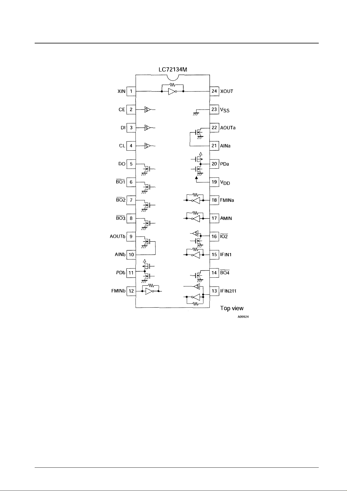
Pin Assignments
No. 5814-2/27
LC72134M

No. 5814-3/27
LC72134M
Block Diagram
No. 5814-4/27
LC72134M
Parameter Symbol Conditions Ratings Unit
Maximum supply voltage V
DD
max V
DD
–0.3 to +7.0 V
V
IN
1 max CE, DI, CL, AINa, AINb –0.3 to +7.0 V
Maximum input voltage V
IN
2 max XIN, FMINa, FMINb, AMIN, IFIN1, IFIN2/I1 –0.3 to VDD+0.3 V
V
IN
3 max IO2 –0.3 to +15 V
V
O
1 max DO –0.3 to +7.0 V
Maximum output voltage V
O
2 max XOUT, PDa, PDb –0.3 to VDD+0.3 V
V
O
3 max BO1 to BO4, IO2, AOUTa, AOUTb –0.3 to +15 V
I
O
1 max BO1 0 to +3.0 mA
Maximum output current I
O
2 max DO, AOUTa, AOUTb 0 to +6.0 mA
I
O
3 max BO2 to BO4, IO2 0 to +10.0 mA
Allowable power dissipation Pd max Ta ≤ 85°C 200 mW
Operating temperature Topr –40 to +85 °C
Storage temperature Tstg –55 to +125 °C
Specifications
Absolute Maximum Ratings at Ta = 25°C, VSS= 0 V
Parameter Symbol Conditions
Ratings
Unit
min typ max
Supply voltage V
DDVDD
4.5 5.5 V
V
IH
1 CE, DI, CL 0.7 V
DD
6.5 V
Input high-level voltage V
IH
2 IFIN2/I1 0.7 V
DD
V
DD
V
V
IH
3 IO2 0.7 V
DD
13 V
Input low-level voltage V
IL
CE, DI, CL, IO2, IFIN2/I1 0 0.3 V
DD
V
Output voltage
V
O
1 DO 0 6.5 V
V
O
2 BO1 to BO4, IO2, AOUTa, AOUTb 0 13 V
f
IN
1 XIN: VIN1 1 8 MHz
f
IN
2 FMINa, FMINb: VIN2 10 160 MHz
Input frequency f
IN
3 AMIN: VIN3, SNS = 1 2 40 MHz
f
IN
4 AMIN: VIN4, SNS = 0 0.5 10 MHz
f
IN
5 IFIN1, IFIN2/I1: VIN5 0.4 25 MHz
V
IN
1 XIN: fIN1 400 1500 mVrms
V
IN
2-1 FMINa, FMINb: f = 10 to 130 MHz 40 1500 mVrms
V
IN
2-2 FMINa, FMINb: f = 130 to 160 MHz 70 1500 mVrms
Input amplitude V
IN
3 AMIN: fIN3, SNS = 1 40 1500 mVrms
V
IN
4 AMIN: fIN4, SNS = 0 40 1500 mVrms
V
IN
5 IFIN1, IFIN2/I1: f = 0.4 to 25 MHz, IFS = 1 70 1500 mVrms
V
IN
6 IFIN1, IFIN2/I1: f = 0.4 to 12 MHz, IFS = 0 100 1500 mVrms
Guaranteed crystal oscillator frequency Xtal XIN, XOUT: *1 4.0 8.0 MHz
Allowable Operating Ranges at Ta = –40 to 85°C, VSS= 0 V
Note: Recommended value for CI for the crystal oscillator element: CI ≤ 120 Ω (4.5 MHz) or CI ≤ 70 Ω (7.2 MHz)
However, since the oscillator circuit characteristics depend on the printed circuit board, circuit constants, and other factors, consult with the
manufacturer of the crystal element.
Parameter Symbol Conditions
Ratings
Unit
min typ max
Rf1 XIN 1.0 MΩ
Internal feedback resistance
Rf2 FMINa, FMINb 500 kΩ
Rf3 AMIN 500 kΩ
Rf4 IFIN1, IFIN2/I1 250 kΩ
Internal pull-down resistance
Rpd1 FMINa, FMINb 200 kΩ
Rpd2 AMIN 200 kΩ
Hysteresis V
HIS
CE, DI, CL, IO2, IFIN2/II 0.1 V
DD
V
Output high-level voltage V
OH
1 PDa, PDb: IO= –1 mA VDD– 1.0 V
Electrical Characteristics in the Allowable Operating Ranges
Continued on next page.
No. 5814-5/27
LC72134M
Parameter Symbol Conditions
Ratings
Unit
min typ max
V
OL
1 PDa, PDb: IO= 1 mA 1.0 V
V
OL
2
BO1: I
O
= 0.5 mA 0.5 V
BO1: I
O
= 1 mA 1.0 V
V
OL
3
DO: I
O
= 1 mA 0.2 V
Output low-level voltage DO: I
O
= 5 mA 1.0 V
BO2 to BO4, IO2: I
O
= 1 mA 0.2 V
V
OL
4 BO2 to BO4, IO2: IO= 5 mA 1.0 V
BO2 to BO4, IO2: I
O
= 8 mA 1.6 V
V
OL
5 AOUTa, AOUTb: IO= 1 mA, AIN = 1.3 V 0.5 V
I
IH
1 CE, DI, CL: VI= 6.5 V 5.0 µA
I
IH
2 IFIN2/I1: VI= VDD, L/I1 = 0 5.0 µA
I
IH
3 IO2: VI= 13 V 5.0 µA
Input high-level current I
IH
4 XIN: VI= V
DD
2.0 11 µA
I
IH
5 FMINa, FMINb, AMIN: VI= V
DD
4.0 22 µA
I
IH
6 IFIN1, IFIN2/I1: VI= V
DD
8.0 44 µA
I
IH
7 AINa, AINb: VI= 6.5 V 200 nA
I
IL
1 CE, DI, CL: VI= 0 V 5.0 µA
I
IL
2 IFIN2/I1: VI= 0 V, L/I1 = 0 5.0 µA
I
IL
3 IO2: VI= 0 V 5.0 µA
Input low-level current I
IL
4 XIN: VI= 0 V 2.0 11 µA
I
IL
5 FMINa, FMINb, AMIN: VI= 0 V 4.0 22 µA
I
IL
6 IFIN1, IFIN2/I1: VI= 0 V 8.0 44 µA
I
IL
7 AINa, AINb: VI= 0 V 200 nA
Output off leakage current
I
OFF
1 BO1 to BO4, AOUTa, AOUTb, IO2: VO= 13 V 5.0 µA
I
OFF
2 DO: VO= 6.5 V 5.0 µA
High-level 3-state off leakage current I
OFFH
PDa, PDb: VO= V
DD
0.01 200 nA
Low-level 3-state off leakage current I
OFFL
PDa, PDb: VO= 0 V 0.01 200 nA
Input capacitance C
IN
FMINa, FMINb 6 pF
I
DD
1
V
DD
: Crystal = 7.2 MHz, fIN2 = 130 MHz
5 10 mA
(FMINa operating), V
IN
2 = 40 mV rms
V
DD
: Crystal = 7.2 MHz, fIN2 = 130 MHz
I
DD
2 (FMINa and FMINb operating), 8 16 mA
Current drain
V
IN
2 = 40 mV rms
V
DD
: PLL block stopped (PLL INHIBIT mode)
I
DD
3 Crystal oscillator operating 0.5 mA
(crystal frequency: 7.2 MHz)
I
DD
4
V
DD
: PLL block stopped, crystal oscillator
10 µA
stopped
Continued from preceding page.
Pin Descriptions
Pin Pin No. Type Function Equivalent circuit
Xtal • Crystal oscillator element connections (4.5 or 7.2 MHz)
XIN
XOUT
1
24
Main PLL
local oscillator
signal input
• FMINa is selected when DVS in the serial data is set to 1.
• Input frequency: 10 to 160 MHz
• The signal is passed through an internal divide-by-two prescaler and then input to
the swallow counter.
• The divisor can be set to a value in the range 272 to 65535. Since the internal
divide-by-two prescaler is used, the actual divisor will be twice the set value.
FMINa 18
Continued on next page.

No. 5814-6/27
LC72134M
Continued from preceding page.
Pin Pin No. Type Function Equivalent circuit
Main PLL
local oscillator
signal input
• AMIN is selected when DVS in the serial data is set to 0.
• When SNS in the serial data is set to 1:
• Input frequency: 2 to 40 MHz
• The signal is input to the swallow counter directly.
• The divisor can be set to a value in the range 272 to 65535. The set value
becomes the actual divisor.
• When SNS in the serial data is set to 0:
• Input frequency: 0.5 to 10 MHz
• The signal is input to a 12-bit programmable divider directly.
• The divisor can be set to a value in the range 5 to 4095. The set value becomes
the actual divisor.
AMIN 17
Chip enable
• This pin must be set high to enable serial data input (DI) or serial data output
(DO).
CE 2
Input data • Input for serial data transferred from the controllerDI 3
Clock
• Clock used for data synchronization for serial data input (DI) and serial data
output (DO).
CL 4
Output data
• Output for serial data transmitted to the controller. The content of the data
transmitted is determined by DOC0 through DOC2.
DO 5
Power supply
• LC72134M power supply (V
DD
= 4.5 to 5.5 V)
• The power on reset circuit operates when power is first applied.
——
V
DD
19
Ground • LC72134M ground ——
V
SS
23
Output ports
• Output-only ports
• The output state is determined by BO1 through BO4 in the serial data.
When the data value is 0: The output state will be the open circuit state.
When the data value is 1: The output state will be a low level.
• A time base signal (8 Hz) is output from BO1 when TBC in the serial data is set to
1.
BO1
BO2
BO3
BO4
6
7
8
14
I/O port
• Shared function I/O port
• The pin function is determined by IOC2 in the serial data.
When the data value = 0: Input port
When the data value = 1: Output port
• When specified to function as an input port:
The input pin state is reported to the controller through the DO pin.
When the input state is low: The data will be 0:
When the input state is high: The data will be 1:
• When specified to function as an output port:
The output state is determined by IO2 in the serial data.
When the data value is 0: The output state will be the open circuit state.
When the data value is 1: The output state will be a low level.
• This pin is set to input mode after a power on reset.
IO2 16
Main PLL
charge pump
output
• PLL charge pump output
A high level is output when the frequency of the local oscillator signal divided by N
is higher than the reference frequency, and a low level is output when that
frequency is lower. This pin goes to the high-impedance state when the
frequencies match.
PDa 20
Main PLL lowpass filter
amplifier
transistor
• Connections for the n-channel MOS transistor to be used for the PLL active lowpass filter.
AINa
AOUTa2122
Continued on next page.

No. 5814-7/27
LC72134M
Continued from preceding page.
Pin Pin No. Type Function Equivalent circuit
IF counter 1
• IFIN1 is selected when LCTS in the serial data is set to 0.
• The input frequency range is 0.4 to 25 MHz when IFS is 1, and 0.4 to 12 MHz
when IFS is 0.
• The signal is passed directly to the IF counter.
• The result is output, MSB first, through the DO pin.
• Four measurement periods are supported: 4, 8, 32, and 64 ms.
IFIN1 15
IF counter 2
input port
• IFIN2 is selected when both LCTS and L/I1 in the serial data are set to 1.
• The input frequency range is 0.4 to 25 MHz when IFS is 1 and 0.4 to 12 MHz
when IFS is 0.
• The signal is passed directly to the IF counter.
• The result (the IF counter value) is output, MSB first, through the DO pin.
• Four measurement periods are supported: 4, 8, 32, and 64 ms.
• If the L/I1 bit in the serial data is set to 0, the IFIN2/I1 port will function as an input
port and the state of the input pin will be reported to the microcontroller from the
DO pin. (Note that the LCTS value is ignored in this case.)
When the input state is low: the data will be 0:
When the input state is high: the data will be 1:
IFIN2/I1 13
Sub PLL local
oscillator
signal input
• FMINb is selected when SDVS in the serial data is set to 1.
• The input frequency range is 10 to 160 MHz.
• The signal is passed through an internal divide-by-two prescaler and then input to
the swallow counter.
• The divisor can be set to a value in the range 272 to 8191. Since the internal
divide-by-two prescaler is used, the actual divisor will be twice the set value.
• FMINb goes to the stopped state (pulled down) when SDVS in the serial data is
set to 0.
FMINb 12
Sub PLL
charge pump
output
• Sub PLL charge pump output
A high level is output from the PD pin when the frequency of the local oscillator
signal divided by N is higher than the reference frequency, and a low level is
output when that frequency is lower. This pin goes to the high-impedance state
when the frequencies match.
PDb 11
Sub PLL lowpass filter
amplifier
transistor
• Connections for the n-channel MOS transistor used for the sub PLL active lowpass filter.
AINb
AOUTb
10
9

Procedures for Input and Output of Serial Data
This product uses the CCB (Computer Control Bus), which is Sanyo’s audio product serial bus format, for data input and
output. This product adopts an 8-bit address CCB format.
No. 5814-8/27
LC72134M
I/O mode
Address
Function
B0 B1 B2 B3 A0 A1 A2 A3
• Control data input (serial data input) mode
1 IN1 (82) 0 0 0 1 0 1 0 0
• 24 bits of data are input.
• See the “DI Control Data (serial data input)” section for details on the
content of the input data.
• Control data input (serial data input) mode
2 IN2 (92) 1 0 0 1 0 1 0 0
• 24 bits of data are input.
• See the “DI Control Data (serial data input)” section for details on the
content of the input data.
• Control data input (serial data input) mode
3 IN3 (B2) 1 1 0 1 0 1 0 0
• 24 bits of data are input.
• See the “DI Control Data (serial data input)” section for details on the
content of the input data.
• Data output (serial data output) mode
4 OUT (A2) 0 1 0 1 0 1 0 0
• The number of bits output is equal to the number of clock cycles.
• See the “DO Control Data (serial data output)” section for details on the
content of the output data.

Structure of the DI Control Data (serial data input)
• IN1 (Main PLL/Latch-a)
• IN2 (Main PLL/Latch-a)
• IN3 (Sub PLL/Latch-b)
No. 5814-9/27
LC72134M
IN 1
IN 2
IN 3

No. 5814-10/27
LC72134M
DI Control Data
No. Control block/data Function Related data
1
Main PLL
programmable
divider data
P0 to P15
DVS, SNS
• Specifies the divider for the main PLL programmable divider.
This is a binary value in which P15 is the MSB. The position of the LSB changes depending on DVS and
SNS.
(* : don’t care)
* LSB: When P4 is the LSB, P0 to P3 are ignored.
2
Main PLL reference
divider data
R0 to R3
XS
• Selects the reference frequency for the main PLL
* PLL INHIBIT mode
In this mode, the main PLL programmable divider is stopped, the FMINa and AMIN pins are pulled down
to ground, and the main PLL charge pump output goes to the high-impedance state.
* Crystal oscillator stop mode
The crystal oscillator circuit is stopped.
Therefore applications must not select this mode while the sub PLL is operating.
• Crystal oscillator element selection data
XS = 0: 4.5 MHz
XS = 1: 7.2 MHz
Note that 7.2 MHz is selected after a power on reset.
DVS SNS LSB Set divisor (N) Actual divisor
1 * P0 272 to 65535 Twice the set value
0 1 P0 272 to 65535 The set value
0 0 P4 4 to 4095 The set value
R3 R2 R1 R0 Reference frequency
0 0 0 0 100 kHz
0 0 0 1 50
0 0 1 0 25
0 0 1 1 25
0 1 0 0 12.5
0 1 0 1 6.25
0 1 1 0 3.125
0 1 1 1 3.125
1 0 0 0 10
1 0 0 1 9
1 0 1 0 5
1 0 1 1 1
1 1 0 0 3
1 1 0 1 15
1 1 1 0 PLL INHIBIT + X’tal OSC STOP
1 1 1 1 PLL INHIBIT
• These pins select the signal input to the main PLL programmable divider (FMINa or AMIN) and switch the
input frequency range.
* See the “Structure of the Programmable Divider” section for details.
DVS SNS Input pin Frequency range accepted by the input pin
1 * FMINa 10 to 160 MHz
0 1 AMIN 2 to 40 MHz
0 0 AMIN 0.5 to 10 MHz
(* : don’t care)
Continued on next page.

No. 5814-11/27
LC72134M
No. Control block/data Function Related data
3
4
IF counter control
data
CTE
GT0, GT1
IF counter selection
data
LCTS
L/I1
I/O port setup data
IOC2
• IF counter measurement start command data
CTE = 1: Starts the counter
CTE = 0: Resets the counter
• Determines the IF counter measurement time.
• Specifies input or output for the shared function I/O pin (IO2).
Data = 0: Input port
Data = 1: Output port
5
Output port data
BO1 to BO4
IO2
• Determines the output state of the BO1 through BO4 and IO2 output ports.
Data = 0: Open
Data = 1: Low level
• The data is reset to 0, setting the pins to the open state, after a power on reset.
IOC2
Continued from preceding page.
IFS
GT1 GT0 Measurement time Wait time
0 0 4 ms 3 to 4 ms
0 1 8 3 to 4
1 0 32 7 to 8
1 1 64 7 to 8
LCTS L/I1 IFIN2/I1 pin IFIN1 pin
0 0 I1 (Input port)
IFIN1 (IF counter 1)
0 1
OFF (Pulled down)
1 0 I1 (Input port)
OFF (Pulled down)
1 1
IFIN2 (IF counter 2)
* See the “Structure of the IF Counter” section for details.
• Specifies the IF counter input pin (IFIN1 or IFIN2/I1).
LCTS = 0: IFIN1
LCTS = 1: IFIN2/I1
L/I1 = 0: I1 (Input port)
L/I1 = 1: IFIN2 (IF counter 2)
Continued on next page.

No. Control block/data Function Related data
No. 5814-12/27
LC72134M
Continued from preceding page.
6
DO pin control data
DOC0
DOC1
DOC2
• Determines the DO pin output.
The open state is selected after a power on reset.
*1. end-UC: IF counter measurement end check
(1) When end-UC is selected and an IF count is started (by switching CTE from 0 to 1), the DO pin
automatically goes to the open state.
(2) When the IF counter measurement period completes, the DO pin goes to the low level, allowing
applications to test for the completion of the count period.
(3) The DO pin is set to the open state by performing a serial data input or output operation (when the
CE pin is set high).
*2. Valid when the IFIN2/I1 pin is set to the input port state (L/I1 = 0).
(The DO pin will go to the open state if L/I1 is set to 1.)
*3. Goes to the open state when the IO pin is set to the output state.
Note: During the data input period (the period that CE is high in IN1, IN2, or IN3 mode), the DO pin goes
to the open state regardless of the DO pin control data (DOC0 to DOC2). During the data output
period (the period that CE is high in OUT mode) the DO pin state reflects the internal DO serial
data in synchronization with the CL clock, regardless of the DO pin control data (DOC0 to DOC2).
UL0, UL1
ULa, ULb
CTE
L/I1
IOC2
7
Unlocked state
detection data
UL0, UL1
• Selects the width of the phase error (øE) detected for PLL lock state discrimination. A phase error is
recognized if a phase error in excess of the detection width occurs.
* When the PLL is unlocked, the DO pin goes low and UL in the serial data output is set to 0.
When the PLL is locked, the DO pin goes high and UL in the serial data output is set to 1.
Dead zone width: DZA < DZB < DZC < DZD
DOC0
DOC1
DOC2
BO1
8
Phase comparator
control data
DZ0, DZ1
• Controls the phase comparator dead zone
9
Clock time base
TBC
• Setting the TBC bit to 1 causes an 8-Hz clock time base signal with a 40% duty to be output from the
BO1 pin. (The BO1 data will be ignored.)
DOC2 DOC1 DOC0 DO pin state
0 0 0 Open
0 0 1 Low when the PLL is unlocked
0 1 0 end-UC (See *1 below.)
0 1 1 Open
1 0 0 Open
1 0 1 IFIN2/I1 pin state (*2)
1 1 0 The IO2 pin state (*3)
1 1 1 Open
UL1 UL0 øE detection width Detection output
0 0 Stopped Open
0 1 0 øE is output directly
1 0 ±0.55 µs øE is extended by 1 to 2 ms
1 1 ±1.11 µs øE is extended by 1 to 2 ms
DZ1 DZ0 Dead band mode
0 0 DZA
0 1 DZB
1 0 DZC
1 1 DZD
Continued on next page.

No. 5814-13/27
LC72134M
Continued from preceding page.
No. Control block/data Function Related data
10
Main charge pump
control data
DLC
• Controls the charge pump output (PDa).
* If the circuit deadlocks due to the VCO control voltage (Vtune) being 0 and the VCO being stopped,
applications can get out of the deadlocked state by setting the charge pump output to low and setting
Vtune to V
CC
. (Deadlock clear circuit)
11 IFS
• This data is normally set to 1. Setting this data to 0 sets the circuit to reduced input sensitivity mode, in
which the sensitivity is reduced by about 10 to 30 mV rms.
12
Test data
TEST0 to 2
• Test data
TEST0
TEST1 All these bits must be set to 0.
TEST2
All these bits are set to 0 after a power on reset.
13
*
• This bit must be set to 0.
14
Sub PLL
programmable
divider data
PS0 to 12
SDVS
• Specifies the divisor for the sub PLL programmable divider (FMINb).
This is a binary value in which PS0 is the LSB and PS12 the MSB.
• The divisor can be set to a value in the range 272 to 8191. Since the internal divide-by-two prescaler is
used, the actual divisor will be twice the set value.
• Sets the sub PLL programmable divider operating state.
*: See the “Structure of the Programmable Divider” section for details.
15
Sub PLL charge
pump control data
SDLC
• Forcibly controls the charge pump output (PDb).
* If the circuit deadlocks due to the VCO control voltage (Vtune) being 0 and the VCO being stopped,
applications can get out of the deadlocked state by setting the charge pump output to low and setting
Vtune to V
CC
. (Deadlock clear circuit)
16
Sub PLL reference
divider data
RS0, RS1
• Sub PLL reference frequency (fref) selection data
17
Unlocked state
detection output
switching data
ULa, ULb
• The unlocked state information output from the DO pin can be selected to be that for either the main PLL
or the sub PLL.
DLC Charge pump output
0 Normal operation
1 Forced to low
SDLC Charge pump output
0 Normal operation
1 Forced to low
SDVS Operating state Input pin frequency range
1 The FMINb counter operates
0
The FMINb counter is stopped 10 to 160 MHz
(FMINb is pulled down)
RS1 RS0 Reference frequency
0 0 50 kHz
0 1 25
1 0 12.5
1 1 15
ULb ULa Unlocked state information
0 0 No unlocked state information is output. The output data, UL is 1.
0 1 Main PLL unlocked state information
1 0 Sub PLL unlocked state information
1 1
Main PLL plus sub PLL unlocked state information.
(Indicates that either the main or the sub PLL is unlocked.)

No. 5814-14/27
LC72134M
No. Control block/data Description Related data
1
I/O port data
12, I1
• Data latched from the IFIN2/I1 input port (when L/I1 is 0) and the I/O port IO2 pin. The I2 data reflects the
pin state regardless of the I/O port mode (input or output). The data is latched at the point the circuit enters
data output mode (OUT mode).
The data is latched at the point the circuit enters data output mode (OUT mode).
I1
← IFIN2/I1 pin state H : 1
I2 ← The IO2 pin state L : 0
L/I1
IOC2
Structure of the DO Output Data (serial data output)
• OUT mode
DO Output Data
2
PLL unlocked state
data
UL
• Indicates the state of the unlocked state detection circuit.
UL ← 0: When the PLL is unlocked.
UL ← 1: When the PLL is locked or in the detection disabled mode.
UL0, UL1
ULa, ULb
3
IF counter binary
data
C19 to C0
• Indicates the value of the IF counter (20-bit binary counter).
C19 ← MSB of the binary counter
C0 ← LSB of the binary counter
CTE
GT0
GT1
4
IF counter selection
data
LCT
• Data that reflects the LCTS bit in the serial input data. The LCT output data allows applications to verify the
IF counter input pin selection (IFIN1 or IFIN2).
LCT = 0: IFIN1 selected.
LCT = 1: IFIN2/I1 selected.
LCTS
Serial Data Input (IN1/IN2/IN3) tSU, tHD, tEL, tES, tEH≥ 0.75 µs tLC< 0.75 µs
• CL: Normal (high)

No. 5814-15/27
LC72134M
Serial Data Output (Out) tSU, tHD, tEL, tES, tEH≥ 0.75 µs tDC, tDH< 0.35 µs
• CL: Normal (high)
• CL: Normal (low)
Note: The data conversion times (tDCand tDH) depend on the value of the pull-up resistor and the printed circuit board capacitance since the DO pin is
an n-channel open-drain circuit.
• CL: Normal (low)

Serial Data Timing
No. 5814-16/27
LC72134M
When CL is stopped at the low level
When CL is stopped at the high level
Parameter Symbol Conditions
Ratings
Unit
min typ max
Data setup time t
SU
DI, CL 0.75 µs
Data hold time t
HD
DI, CL 0.75 µs
Clock low level time t
CL
CL 0.75 µs
Clock high level time t
CH
CL 0.75 µs
CE wait time t
EL
CE, CL 0.75 µs
CE setup time t
ES
CE, CL 0.75 µs
CE hold time t
EH
CE, CL 0.75 µs
Data latch change time t
LC
0.75 µs
Data output time
t
DC
DO, CL
These values differ depending on the value of the pull-up
0.35 µs
t
DH
DO, CE
resistor used and the printed circuit board capacitance
0.35 µs

Structure of the Programmable Divider
Structure of the Main PLL Programmable Divider
Sample Main Programmable Divider Divisor Calculations
• For FM with a step size of 50 kHz (DVS = 1, SNS = *: FMINa selected)
FM RF = 90.0 MHz (IF = +10.7 MHz)
FM VCO = 100.7 MHz
Main PLL fref = 25 kHz (R0 = 1, R1 = 1, R2 = 0, R3 = 0)
100.7 MHz (FM VCO) ÷ 25 kHz (fref) ÷ 2 (for the FMIN 1/2 prescaler) = 2014 → 07DE (hexadecimal)
*: Don’t care
No. 5814-17/27
LC72134M
DVS SNS Input pin Set divisor Actual divisor Input frequency range
A 1 * FMINa 272 to 65535 Twice the set value 10 to 160 MHz
B 0 1 AMIN 272 to 65537 The set value 2 to 40 MHz
C 0 0 AMIN 4 to 4095 The set value 0.5 to 10 MHz
• For SW with a step size of 5 kHz (DVS = 0, SNS = 1: AMIN high-speed operation selected)
SW RF = 21.75 MHz (IF = +450 kHz)
SW VCO = 22.20 MHz
Main PLL fref = 5 kHz (R0 = 0, R1 = 1, R2 = 0, R3 = 1)
22.2 MHz (SW VCO) ÷ 5 kHz (fref) = 4440 → 1158 (hexadecimal)
• For MW with a step size of 10 kHz (DVS = 0, SNS = 0: AMIN low-speed operation selected)
MW RF = 1000 kHz (IF = +450 kHz)
WM VCO = 1450 kHz
Main PLL fref = 10 kHz (R0 = 0, R2 = 0, R3 = 1)
1450 kHz (MW VCO) ÷ 10 kHz (fref) = 145 → 091 (hexadecimal)

No. 5814-18/27
LC72134M
Structure of the Sub PLL Programmable Divider
Sample Sub PLL Programmable Divider Divisor Calculations
• For FM with a step size of 100 kHz (SDVS = 1: FMINb operating)
FM RF = 90.0 MHz (IF = –10.7 MHz)
FM VCO = 79.3 MHz
Sub PLL fref = 50 kHz (RS0 = 0, RS1 = 0)
79.3 MHz (FM VCO) ÷ 50 kHz (fref) ÷ 2 (for the FMINb 1/2 prescaler) = 793 → 0319 (hexadecimal)
SDVS Operating state Set divisor Actual divisor: N Input frequency range
1 FMINb operating 272 to 8191 Twice the set value 10 to 160 MHz
0 FMINb stopped (pulled down) — — —
• For FM with a step size of 50 kHz (SDVS = 1: FMINb operating)
FM RF = 90.0 MHz (IF = +10.7 MHz)
FM VCO = 100.7 MHz
Sub PLL fref = 25 kHz (RS0 = 1, RS1 = 0)
100.7 MHz (FM VCO) ÷ 25 kHz (fref) ÷ 2 (for the FMINb 1/2 prescaler) = 2014 → 07DE (hexadecimal)

Structure of the IF Counter
The LC72134M IF counter is a 20-bit binary counter, and takes the IF signal from the IFIN1 or IFIN2/I1 pin as its input.
The result of the count can be read out serially MSB first from the DO pin.
The IF frequency (FC) is measured by determining how many pulses were input to the IF counter in the stipulated measurement time, GT.
C
Fc = —— (C = Fc × GT) C: Counted value (the number of pulses)
GT
No. 5814-19/27
LC72134M
GT1 GT0
Measurement time
Measurement time (GT) Wait time (t
WU
)
0 0 4 ms 3 to 4 ms
0 1 8 3 to 4
1 0 32 7 to 8
1 1 64 7 to 8
IF Counter Frequency Measurement Examples
• When the measurement time (GT) is 32 ms and the counted value (C) is 53980 (hexadecimal) or 342,400 decimal.
IF frequency (FC) = 342400 ÷ 32 ms = 10.7 MHz
• When the measurement time (GT) is 8 ms and the counted value (C) is E10 (hexadecimal) or 3600 decimal.
IF frequency (FC) = 3600 ÷ 8 ms = 450 kHz

IF Counter Operation
Applications must first, before starting an IF count operation reset the IF counter by setting CTE in the serial data to 0.
The IF counter operation is started setting CTE in the serial data from 0 to 1. Although the serial data is determined by dropping the CE pin from high to low,
the IF signal input to the IFIN pin must be provided within the wait time from the point CE goes low. Next, the readout of the IF counter after measurement is
complete must be performed while CTE is still 1, since the counter will be reset if CTE is set to 0.
Note: If IF counting is used, applications must determine whether or not the IF IC SD (station detect) signal is present in the microcontroller software, and
perform the IF count only if that signal is asserted. This is because auto-search techniques that only use IF counting are subject to incorrect stopping at
points where there is no station due to IF buffer leakage.
Unlocked State Detection Timing
• Unlocked state detection timing
Unlocked state detection is performed during the reference frequency (fref) period (interval). This means that a period
at least as long as the period of the reference frequency is required to recognize the locked/unlocked state. However,
applications must wait at least twice the period of the reference frequency immediately after changing the divisor (N)
(which is applied to the frequency) before checking the locked/unlocked state.
No. 5814-20/27
LC72134M
Figure 1 Unlocked State Detection Timing
For example, if fref is 1 kHz (a period of 1 ms) applications must wait at least 2 ms after the divisor N is changed
before performing a locked/unlocked check.

No. 5814-21/27
LC72134M
Figure 2 Circuit Structure
Figure 3 Combining with Software

• Directly outputting the unlocked state to the DO pin
Since the unlocked state (high level when locked, low when unlocked) is output from the DO pin, the dummy data
processing described above is not necessary. After N is changed, applications can check the locked state after waiting
at least two periods of the reference frequency.
Clock Time Base Usage Notes
When using the clock time base output function, the output pin (BO1) pull-up resistor must have a value of over 100 kΩ.
The use of a Schmitt input in the microcontroller that accepts this signal is recommended to reduce chattering. This is to
prevent degradation of the VCO C/N characteristics when combining with a loop filter that uses the internal transistor
provided to form a low-pass filter. Since the ground for the clock time base output pin and the ground for the transistor
are common internally on the chip, applications must take care to minimize current fluctuations in the time base pin to
prevent degradation of the low-pass filter characteristics.
No. 5814-22/27
LC72134M
Wait at least 2 reference frequency periods
Valid output data is acquired by using an interval of at
least one reference frequency period
*: Even more reliable recognition of the locked state
can be achieved by performing several checks of the
state and requiring that the locked state be detected
sequentially
Divisor N changed (data input)
Dummy data output
Valid data output
Locked state check*
YES
NO
• Outputting the unlocked state data in the serial data
In the LC72134M, the unlocked state data (UL), once set to the unlocked state, is not reset unless data is output (or
input). At the point of data output (1) in figure 3, the VCO frequency will be stable (locked), but since the divisor N
was changed and a data output operation has not yet been performed, the unlocked state data will indicate the unlocked
state. Thus even though the loop is stable (locked), the data will indicate that it is not. In cases such as this, the
application should treat the first data output after the value of N has been changed as dummy data, and consider the
second data output (at point (2) in the figure) as valid data.
<Flowchart for Lock Detection>
A09968

No. 5814-23/27
LC72134M
Other Items
• Notes on the phase comparator dead zone
When the charge pump is used with one of the ON/ON modes, correction pulses are generated from the charge pump
even if the PLL is locked. As a result, it is easy for the loop to become unstable, and special care is required in
application design. The following problems can occur if an ON/ON mode is used.
— Sidebands may be created by reference frequency leakage.
— Sidebands may be created by low-frequency leakage due to the correction pulse envelope.
Although the loop is more stable when a dead zone is present (i.e. when an OFF/OFF mode is used), a dead band
makes it more difficult to achieve excellent C/N characteristics. On the other hand, while it is easy to achieve good C/N
characteristics when there is no dead zone, achieving good loop stability is difficult. Accordingly, the DZA and DZB
settings, in which there is no dead zone, can be effective in situations where a signal-to-noise ratio of 90 to 100 dB or
higher is required in FM reception, or where it is desirable to increase the pilot margin in AM stereo reception.
However, if such a high signal-to-noise ratio is not required for FM reception, if an adequate pilot margin can be
acquired in AM stereo reception, or if AM stereo is not required, then either DZC or DZD, in which there is a dead
band, should be chosen.
DZ1 DZ0 Dead band mode Charge pump Dead band
0 0 DZA ON/ON – –0s
0 1 DZB ON/ON –0s
1 0 DZC OFF/OFF +0s
1 1 DZD OFF/OFF + +0s
≥

No. 5814-24/27
LC72134M
Dead Zone
As shown in figure 1, the phase comparator compares a reference frequency (fr) with fp. As shown in figure 2, the phase
comparator’s characteristics consist of an output voltage (V) that is proportional to the phase difference ø. However, due
to internal circuit delay and other factors, an actual circuit has a region (the dead zone, B) where the circuit cannot
actually compare the phases. To implement a receiver with a high S/N ratio, it is desirable that this region be as small as
possible. However, it is often desirable to have the dead zone be slightly wider in popularly-priced models. This is
because in certain cases, such as when there is a strong RF input, popularly-priced models can suffer from mixer to VCO
RF leakage that modulates the VCO. When the dead zone is small, the circuit outputs signals to correct this modulation
and this output further modulates the VCO. This further modulation may then generate beats with the RF signal.
• Notes on the FMIN, AMIN, and IFIN pins
Coupling capacitors should be placed as close to their pin as possible. A capacitance of about 100 pF is desirable for
these capacitors. In particular, if the IFIN pin coupling capacitor is not held to under 100 pF, the time to reach the bias
level may become too long and incorrect counts may result due to the relationship with the wait time.
• Notes on IF counting → Use the SD signal in conjunction with IF counting
When counting the IF frequency, the microcontroller must determine the presence or absence of the IF IC SD (station
detect) signal and turn on the IF counter buffer output and execute the IF count only if there is an SD signal. Autosearch techniques that only use the IF counter are subject to incorrect stopping at points where there is no station due to
IF buffer leakage.
• DO pin usage
The DO pin can be used for IF counter count completion checking and as an unlock detection output in addition to its
use in data output mode. It is also possible to have the DO pin reflect the state of an input pin to input that state to the
microcontroller.
• Power supply pins
A capacitor of at least 2000 pF must be inserted between the power supply VDDand VSSpins for noise exclusion. This
capacitor must be placed as close as possible to the VDDand VSSpins.
Figure 1 Figure 2

No. 5814-25/27
LC72134M
Pin States after a Power on Reset

Sample Application Circuits
FM/AM Tuner + FM Tuner (for FM Subcarrier)
No. 5814-26/27
LC72134M
Since the areas enclosed in dotted lines ( ) are high-impedance circuits, they are susceptible to noise.
Therefore, lines in the printed circuit board pattern should be made as short as possible and these areas
should be surrounded by the ground pattern.
Note:

PS No. 5814-27/27
LC72134M
This catalog provides information as of March, 1998. Specifications and information herein are subject to
change without notice.
■ No products described or contained herein are intended for use in surgical implants, life-support systems, aerospace
equipment, nuclear power control systems, vehicles, disaster/crime-prevention equipment and the like, the failure of
which may directly or indirectly cause injury, death or property loss.
■ Anyone purchasing any products described or contained herein for an above-mentioned use shall:
➀ Accept full responsibility and indemnify and defend SANYO ELECTRIC CO., LTD., its affiliates, subsidiaries and
distributors and all their officers and employees, jointly and severally, against any and all claims and litigation and all
damages, cost and expenses associated with such use:
➁ Not impose any responsibility for any fault or negligence which may be cited in any such claim or litigation on
SANYO ELECTRIC CO., LTD., its affiliates, subsidiaries and distributors or any of their officers and employees
jointly or severally.
■ Information (including circuit diagrams and circuit parameters) herein is for example only; it is not guaranteed for
volume production. SANYO believes information herein is accurate and reliable, but no guarantees are made or implied
regarding its use or any infringements of intellectual property rights or other rights of third parties.
AM Tuner + FM Tuner
Since the areas enclosed in dotted lines ( ) are high-impedance circuits, they are susceptible to noise.
Therefore, lines in the printed circuit board pattern should be made as short as possible and these areas
should be surrounded by the ground pattern.
Note:
 Loading...