

Page 1
Ordering number: EN 3356A
CMOS IC
LC7185-8750
CB Transceiver PLL Frequency Synthesizer
and Controller
Overview
This 27 MHz band, PLL frequency synthesizer LSI chip is
designed specifically for CB transceivers.
The specifications are suited for use in U.S.A.(FCC).
Functions
The LC7185-8750 incorporates PLL circuitry and a controller
for CB applications on a single CMOS chip. The controller
handles the PLL circuitry, frequency data ROM, channel
preset/recall RAM, and LED display driver. It also supports
channel scan, channel preset/recall, and emergency channel
call.
Features
1. A built-in programmable divider for the 16 MHz VCO
2. Transmission is inhibited when the PLL is unlocked (digital
lock monitor).
3. Direct channel 9 or 19 selection (sliding switch)
4. A 7-segment, 2-character LED display
5. ‘‘PA’’ is displayed in public announcement mode.
6. Output beep-tone control circuitry
7. Up to 5 channel settings can be stored in memory.
8. 4 × 3 key matrix implementation
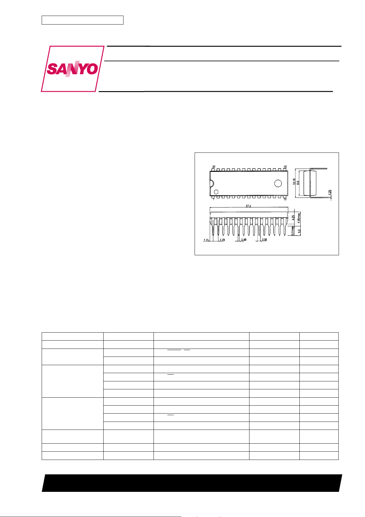
Package Dimensions
unit : mm
3061-DIP30S
[LC7185-8750]
SANYO : DIP30S (400 mil)
Specifications
Absolute Maximum Ratings at Ta = 25°C, VSS=0V
Parameter Symbol Conditions Ratings Unit
Maximum supply voltage V
Input voltage V
Output voltage V
Output Current I
Allowable power
dissipation
Operating temperature Topr –40 to +85 °C
Storage temperature Tstg –55 to +125 °C
max Pin V
DD
1 max Pins HOLD, TX –0.3 to +15 V
IN
V
2 max Input pins other than VIN1 max –0.3 to VDD+0.3 V
IN
1 max Pins SA, SB, SC, SD, SE, SF, SG, D1, D2 –0.3 to +15 V
O
V
2 max Pins UL, BEEP –0.3 to +15 V
O
V
3 max Pin PD –0.3 to VDD+0.3 V
O
V
4 max Output pins other than mentioned above –0.3 to VDD+0.3 V
O
1 max Pins SA, SB, SC, SD, SE, SF, SG 0 to +30 mA
O
I
2 max Pins D1, D2 0 to +10 mA
O
I
3 max Pins UL 0 to +20 mA
O
I
4 max Pin BEEP 0 to +10 mA
O
Pd max (Ta % 85°C) 350 mW
DD
–0.3 to +9.0 V
SANYO Electric Co.,Ltd. Semiconductor Bussiness Headquarters
TOKYO OFFICE Tokyo Bldg., 1-10, 1 Chome, Ueno, Taito-ku, TOKYO, 110-8534 JAPAN
73098HA(II)/5220TA No.3356-1/12
Page 2
LC7185-8750
Allowable Operating Conditions at Ta = –40 to +85°C, VSS=0V
Parameter Symbol Conditions min typ max Unit
Supply voltage V
Input high-level voltage
Input low-level voltage
Output voltage
Input frequency
Input amplitude
Required oscillating
frequency
DD
V
1 Pins HOLD, TX 0.7V
IH
V
2 Pin INIT 3.2 V
IH
V
3 Pins KI1, KI2, KI3, KI4 0.6V
IH
1 Pins HOLD, TX 0 0.3V
V
IL
V
2 Pin INIT 0 1.3 V
IL
V
3 Pins KI1, KI2, KI3, KI4 0 0.4V
IL
V
1 Pins SA, SB, SC, SD, SE, SF, SG, D1, D2 0 13 V
OUT
V
2 Pins UL, BEEP 08V
OUT
f
1 Pin XIN (sine wave, capacitor coupled) 1.0 10.24 15 MHz
IN
f
2 Pin PIN (sine wave, capacitor coupled) 10 30 MHz
IN
V
1 Pin XIN (sine wave, capacitor coupled) 0.5 1.5 Vrms
IN
V
2 Pin PIN (sine wave, capacitor coupled) 0.15 1.5 Vrms
IN
X’tal Pins XIN, XOUT (CI % 50 Ω) 5.0 10.24 15 MHz
Electrical Characteristics at under allowable operating conditions
Parameter Symbol Conditions min typ max Unit
Internal feedback resistance
Pull-down resistor RpdN Pins KI1, KI2, KI3, KI4, TEST 30 50 70 kΩ
Input high-level current
Input low-level current
Output high-level voltage
Output low-level voltage
Output leakage current
High-level tristate leakage
current
Low-level tristate leakage
current
Supply current
Rf1 Pin XIN 1.0 MΩ
Rf2 Pin PIN 500 kΩ
I
1 Pins HOLD, TX VI=12V 5.0 µA
IH
I
2 Pin INIT VI=V
IH
I
3 Pin XIN VI=V
IH
I
4 Pin PIN VI=V
IH
1 Pins HOLD, TX VI=V
I
IL
I
2 Pin INIT VI=V
IL
I
3 Pin XIN VI=V
IL
I
4 Pin PIN VI=V
IL
V
1 Pins KO1, KO2, KO3 IO=1mA VDD–2.0 VDD–1.0 VDD–0.5 V
OH
V
2 Pin PD IO= 0.5 mA VDD–1.0 V
OH
V
1 Pins KO1, KO2, KO3 IO= 20 µA 0.6 1.0 1.4 V
OL
V
2 Pin PD IO= 0.5 mA 1.0 V
OL
V
3 Pin BEEP IO= 2 mA 1.0 V
OL
V
V
V
I
OFF
I
OFF
I
OFFH
I
OFFL
I
Pins SA, SB, SC, SD, SE, SF, SG
4
OL
I
=20mA
O
5 Pins D1, D2 IO= 5 mA 1.0 V
OL
6 Pin UL IO=10mA 1.0 V
OL
Pins SA, SB, SC, SD, SE, SF, SG, D1, D2
1
V
=13V
O
2 Pins UL, BEEP VO=8V 5.0 µA
Pin PD VO=V
Pin PD VO=V
Normal mode
1
DD
*1 (PLL operates)
Hold mode V
I
*2 (memory backup)
2
DD
V
DD
= 8.0 V
DD
DD
DD
DD
SS
SS
SS
SS
DD
SS
= 3.2 V
5.0 8.0 V
DD
DD
12 V
DD
V
DD
DD
DD
5.0 µA
25 µA
50 µA
5.0 µA
5.0 µA
25 µA
50 µA
1.0 V
5.0 µA
0.01 10.0 nA
0.01 10.0 nA
510mA
515µA
V
V
V
V
µA
*1: fIN2 = 20 MHz (PIN)
V
2 = 0.15 Vrms
IN
X’tal = 10.240 MHz
TX = HOLD = INIT = V
Other inputs = V
SS
DD
*2: HOLD = V
TX = INIT = V
Other inputs = V
Other outputs = open
SS
DD
SS
Other outputs = open
Note: Be careful that the dielectric strength of pins SA, SB, SC, SD, SE, SF, D1, D2, UL, BEEP are weak.
No. 3356-2/12
Page 3
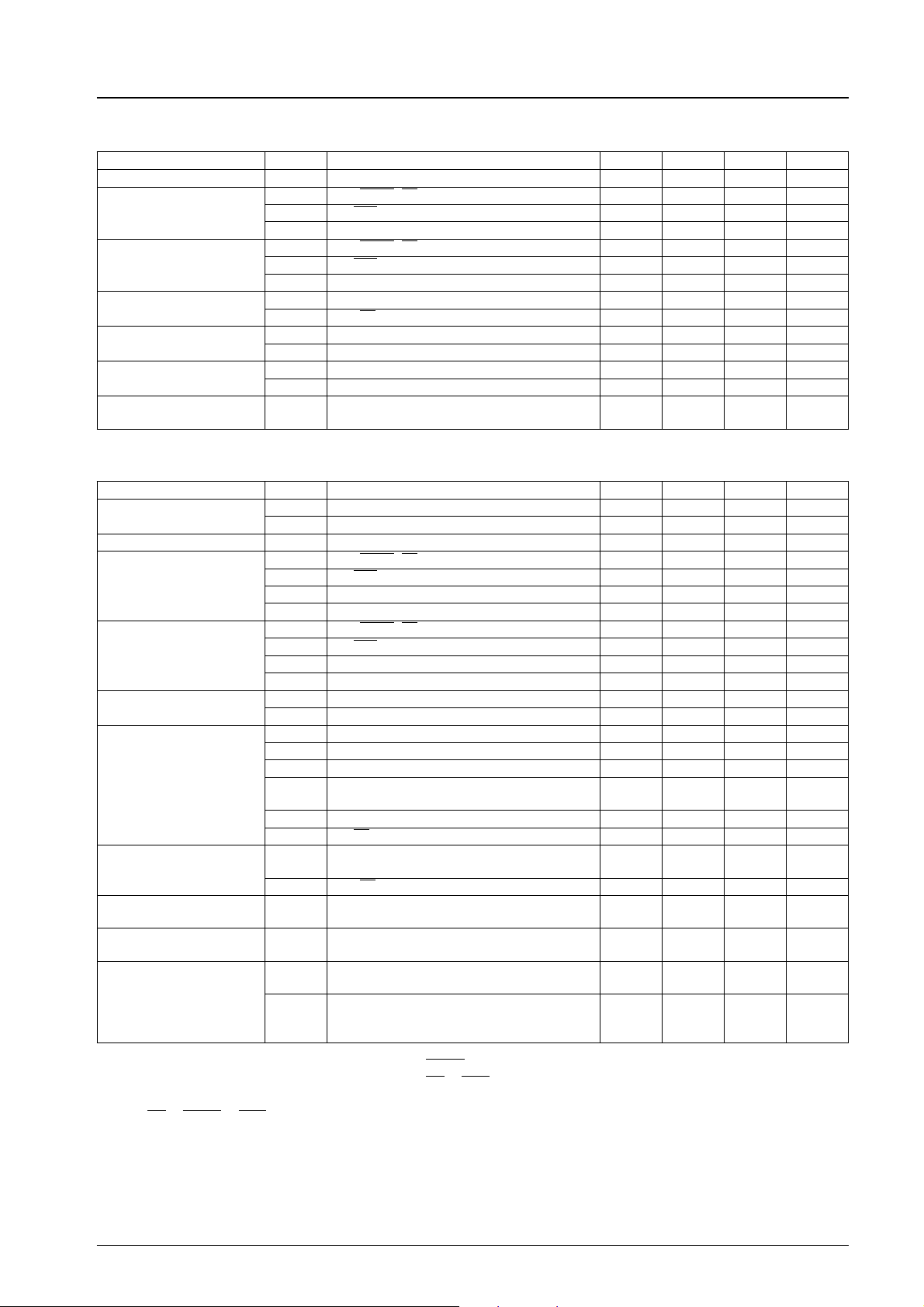
Pin Assignment
Block Diagram
LC7185-8750
No. 3356-3/12
Page 4
LC7185-8750
Pin Descriptions
TX Transmit/receive select PD Charge pump output
HOLD
INIT
TEST Test point (input) D1, D2 Digit output (for display)
V
PIN Programmable divider input KO1 to KO3 Key scan outputs
XIN, XOUT Crystal oscillator input, output
UL
1, VSS2 Power supply KI1 to KI4 Key inputs
DD,VSS
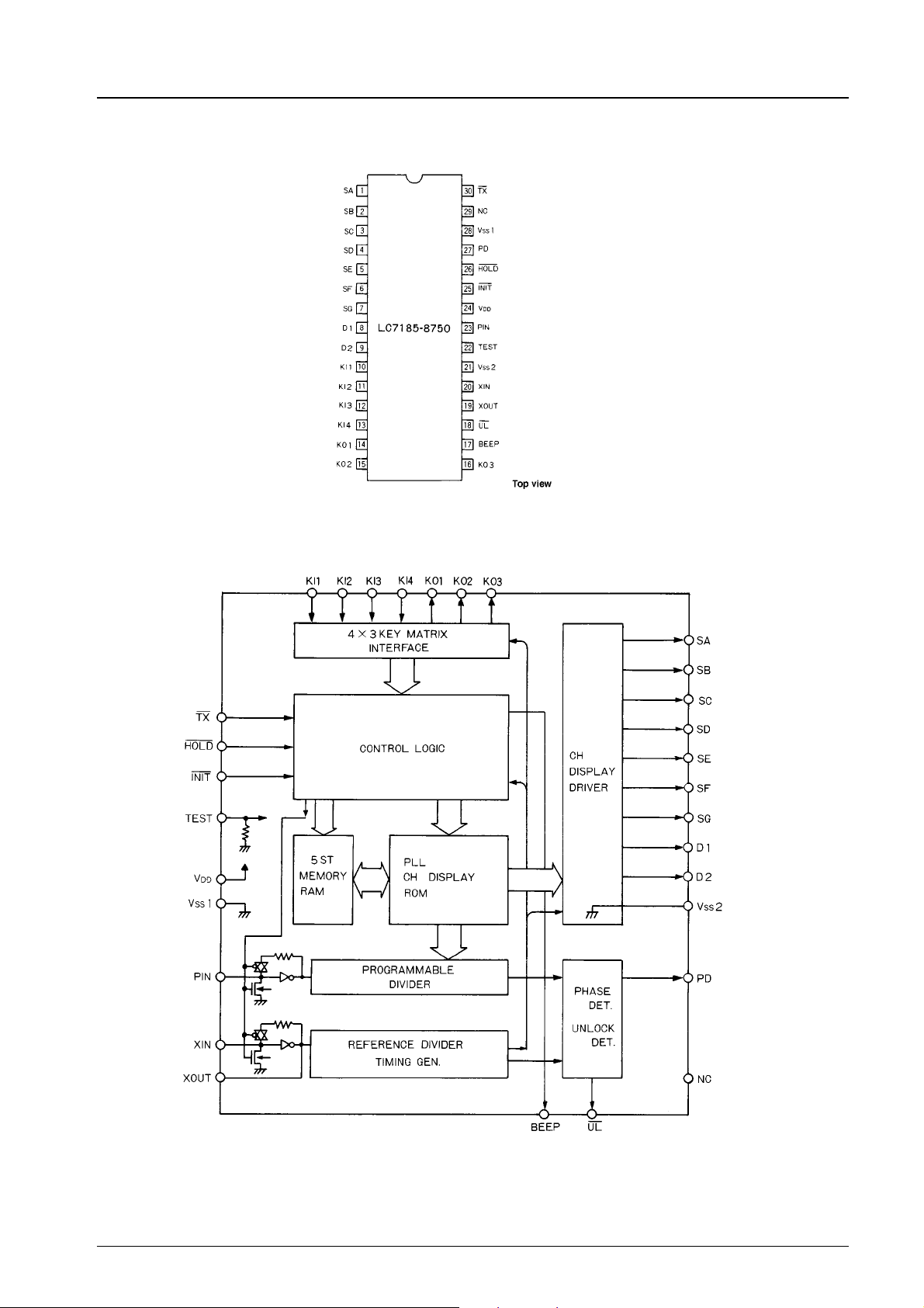
Key Matrix
Hold mode select NC NC pin
Initial input SAto SG Segment driver (for display)
BEEP Beep-tone control output
(10.240 MHz)
Unlock detection signal output
CH9 Emergency CH9 recall ME Station Memory Enable
CH19 Emergency CH19 recall M1 to M5 Station Memory recall
PA Public announcement display UP/DN/ME/M1 to 5 Momentary SW
MODE 1/2 Display Mode CH9/CH19/PA Slide SW
UP CH up/scan MODE 1/2 Diode
DN CH down/scan
LED Display Configuration (Common anode/7 segment)
No. 3356-4/12
Page 5

LC7185-8750
Pin Description
Pin Name Pin No. Type Description
TX
HOLD 26
INIT
TEST 22
30
25
.
Transmit/receive select
TX = ‘‘0’’...Transmit, TX = ‘‘1’’...Receive
.
Hold mode select
HOLD = ‘‘0’’...Hold mode select
= ‘‘1’’...Normal mode select
.
Reset line
INIT = ‘‘0’’...Reset
.
Test point (input)
Tie to ground or leave floating
V
DD
V
221
SS
PIN 23
XIN
XOUT
PD 27
V
128
SS
NC 29
UL
24
20
19
18
.
Power supply (+)
Normal mode: 5.0 to 8.0 V
Hold mode: ^ 3.2 V
.
Channel display LED driver ground
.
Programmable divider input
150 mVrms min
Hold mode: Programmable divider is disabled.
.
Crystal oscillator
Frequency: 10.24 MHz
Hold mode: Oscillator is disabled.
.
Charge pump output from the phase comparator. If the frequency of fV
(the signal obtained by dividing the PIN input by N) is higher than that of
fR (the reference signal), or if the phase of fV leads that of fR, positive
pulses are output on this pin. If the frequency is lower or the phase lags,
negative pulses are output on this pin. If they match, the pin goes to high
impedance.
.
fV > fR OR leading: Positive Pulses
.
fV < fR OR leading: Negative Pulses
.
fV = fR and phase muched: High impedance
Hold mode: High impedance
.
PLL circuit and controller ground
.
No-connection
.
Unlock detected output
Fixed to low level when unlocked, when changing channels, in PA mode,
or in hold mode.
Open: Locked
BEEP 17
SA to SG 1 to 7
D1
D2
8
9
.
Beep-tone control output
During station memory operation
During I/O on emergency channel
When changing channels
During reset
During hold mode recovery
Fixed to low level in hold mode
.
Segment drivers for the display
(Common anode/7 segments)
.
Digit output (150 Hz) for the display
(common anode/7 segments)
Hold mode: Transistor goes off.
Transistor: Off (50 ms cycle)
—
→ Open
Continued on next page.
No. 3356-5/12
Page 6

LC7185-8750
Continued from preceding page.
Pin Name Pin No. Type Description
KI1 to KI4 10 to 13
.
Key inputs
Input from the key matrix
KO1 to KO3 14 to 16
.
Key scan output (75 Hz)
Output to the key matrix
Hold mode: Low (scanning stops)
Operation
(1) Channel Selection (up/down)
1. Manual scanning (up/down)
Pressing the UP key increments by one channel and pressing the DN key decrements by channel.
When scanning reaches the end of the band, it automatically wraps around to the beginning.
2. Auto scanning (up/down)
Holding the UP (or DN) key down for 500 ms or longer starts auto scanning. For both up and down scanning, each
channel takes 100 ms to scan.
3. The unlock detected line (UL) is asserted (low) when the UP (or DN) key is pressed and deactivated 25 ms after the key
is released.
4. The beep-tone control line (BEEP) is asserted (open) for 50 ms after each new channel is selected.
UP/DN Key
Channel
(2) Selecting an Emergency Channel (CH9/CH19)
1. If the CH9 or CH19 switch is turned on, the LC7185 stores the value of the previous channel and asserts the beep-tone
control line for 50 ms.
2. While the CH9 or CH19 switch is turned on, the LC7185 disables all keys except TX and PA (UP/DN, ME, and M1 to
M5 switches).
3. Even if the CH9 or CH19 switch is turned off while transmitting using the CH9 or CH19 switch, keep the emergency
channel open until the LC7185 is in the receive mode.
4. After the CH9 or CH19 switch is turned back off, the beep-tone control line is asserted for 50 ms and the LC7185
reopens the previous channel.
5. Note the CH9 has a higher priority over CH19. As a result, if both switches are turned on, CH9 will be opened.
6. The UL line is asserted for 25 ms after the CH9 or CH19 switch is turned off or on.
7. Causes either ‘‘9’’ or ‘‘19’’ to blink on the display.
CH9/CH19
Switch
Channel
Lock: Open
No. 3356-6/12
Page 7

LC7185-8750
(3) Public Announcement (PA) Mode
1. When the PA switch is turned on, the LC7185 stores the value of the previous channel and enters the PA mode.
2. While the PA switch is turned on, the LC7185 disables all keys (TX, CH9/CH19, UP/DN, ME, M1 to M5)
3. ‘‘PA’’ is displayed on the channel display.
4. When the PA switch is turned back off, the LC7185 enters the CB mode and reopens the previous channel.
5. The UL line is asserted while the PA switch is turned on.
PAswitch
Channel
(Display)
(4) Transmit/Receive Selection
1. When the TX line is asserted, the LC7185 enters TX mode.
2. If the PA switch is turned on while the LC7185 is in TX mode, the device enters PA mode. However, if any other
switch (other than the PA switch) or key (UP/DN, ME, M1 through M5, CH9, CH19) is pressed while the LC7185 is in
TX mode, that switch or key has no effect.
3. The unlock detected signal is output each time the device switches between transmitting and receiving.
Pin
Lock: Open
(5) Channel Preset/Recall Facility
1. The LC7185 allows up to 5 channels to be preset (assigned to M1 to M5).
.
After a reset (when the power is turned on, etc.), M1 to M5 are assigned to CH33.
2. Recalling preset channels
.
A preset channel is recalled by pressing one of the preset memory keys (M1 to M5) to which the channel was
previously assigned.
.
There are two different display modes as shown below.
Mode 1 (without diode)
Each time a key is pressed (M1 to M5), the new channel is displayed.
Example: Display 21 → 15
key
Mode 2 (with diode)
Each time a key is pressed (M1 to M5), a key mnemonic (‘‘P1’’ to ‘‘P5’’) is displayed for 400 ms, then the new
channel is displayed.
Example: Display 21 → P1 → 15
Key
M1
400 ms
M1
No. 3356-7/12
Page 8

LC7185-8750
3. Presetting channels
.
First select the channel to be preset, then hold down the ME key and press the preset memory key (M1 to M5) to
which you would like to assign the current channel.
In the following cases, a channel will not be preset:
.
M1 to M5 is pressed and in the memory preset mode.
.
Emergency channels CH9 or CH19 are currently selected.
.
The TX line is asserted.
.
The PA switch is turned on (PA mode).
.
The HOLD line is asserted (hold mode).
Even if the above key operations are not performed, the preset mode will be canceled automatically after 9 seconds.
.
There are two different display modes as shown below.
Mode 1 (without diode)
The current channel is displayed throughout the preset process.
ME
ME
→ 15
M1
400 ms
M1
Example: Display 15
Mode 2 (with diode)
Example: Display 15 → PE → P1 → 15
.
Note that if two or more keys are pressed at the same time, priority is assigned as follows:
M1>M2>M3>M4>M5
Key
When the ME key is held down, ‘‘PE’’ is flashed on the display, indicating that presetting is possible. Once a
preset memory key (M1 to M5) is pressed, the key mnemonic (‘‘P1’’ to ‘‘P5’’) is displayed for 400 ms before the
current channel is redisplayed.
Key
(6) Beep-tone Control Output (BEEP pin)
After each of the following events, the BEEP line is asserted for 50 ms:
.
A reset, such as a battery replacement (INIT = 0)
.
Any key press associated with the channel memory
.
Any emergency channel switch activation
.
A new channel is selected
.
Leaving hold mode
(7) Unlock Detected Output (UL pin)
In the following cases, the UL line is asserted.
.
When the phase difference between the programmable and reference divider outputs exceeds 3.2 µs, the UL line is held low
for 6 ms after the last out-of-range phase sample is detected, as shown below.
Phase
difference
pin
.
After a new transmit/receive or channel selection, the UL line is asserted for 25 ms.
.
While the PA switch is turned on, the UL line is asserted during PA mode.
.
The UL pin is open while the device is in the PLL LOCK state (when the phase difference is < 3.2 µs).
No. 3356-8/12
Page 9

LC7185-8750
(8) Key Matrix
It is normal to put diodes in series with the key scanning lines to avoid creating a short with the output lines.
But KO1, KO2 and KO3 lines (key scan signal output) do not need diodes.
Item
Pins KO1,
KO2, KO3
pins
On impedance
Pull-down resistor
Explanation Regarding Power On and Hold Mode
(1) Operation in hold mode
When in hold mode (HOLD = 0), the LC7185-8750 does not accept any operation other than the INIT pin being asserted
(reset). The primary function of hold mode is to maintain the contents of station memory.
.
In hold mode, the programmable divider, crystal oscillator and reference divider are all stopped.
The PD pin (charge pump output) goes to high impedance. The UL pin goes to V
.
The channel display pins D1 and D2 go to high impedance.
.
The BEEP pin goes to VSS.
.
The key scan signal outputs (KO1 to KO3) go to VSS.
When the LC7185-8750 leaves hold mode, the previously selected channel is reopened.
(2) Initial state settings
The LC7185-8750 can be reset to its initial state settings (reset) after the battery has been replaced, etc., by setting INIT = 0.
The initial state that is established by an initial reset is as follows:
.
When the VDDpin turned on, CH9 or CH33 is selected.
.
When the VDDpin operate voltage already, CH9 is selected.
.
All of station memory is set to CH33.
Linear circuit
.
SS
No. 3356-9/12
Page 10

(3) Timing Requirements for Hold Mode
pin
LC7185-8750
pin
Normal mode Hold mode
V
must remain at 5.0 V or higher (crystal oscillator requirement) for 6.0 ms (t HOLD) after the HOLD line is asserted (HOLD
DD
Normal mode
=0(<0.3VDD). After this, VDDmay go as low as 3.2 V.
There are no constraints on timing for the HOLD and V
pins when the chip is leaving hold mode.
DD
The signal can be activated in one of two orders.
If HOLD is already deactivated (> 0.7 V
), the LC7185-8750 leaves hold mode within 2.0 ms after VDDrises to >5.0 V.
DD
If VDDis > 5.0 V, the LC7185-8750 enters normal mode within 2.0 ms after HOLD is deactivated.
(4) Reset Timing
1. Reset timing (e.g. battery replacement)
pin
pin
Note: tINIT should be greater than 1.0 µs.
2. Reset caused by a sudden voltage (VDD) drop
pin
pin
If V
drops momentarily down to less than 3.2 V and rises up to more than 5.0 V t > tINIT (t > 1.0 µs), a reset may be
DD
generated.
No. 3356-10/12
Page 11

Frequency Table (U.S.A.: LC7185-8750)
LC7185-8750
CHANNEL
1 26.965 6508 16.27 5393 13.4825
2 26.975 6512 16.28 5395 13.4875
3 26.985 6516 16.29 5397 13.4925
4 27.005 6524 16.31 5401 13.5025
5 27.015 6528 16.32 5403 13.5075
6 27.025 6532 16.33 5405 13.5125
7 27.035 6536 16.34 5407 13.5175
8 27.055 6544 16.36 5411 13.5275
9 27.065 6548 16.37 5413 13.5325
10 27.075 6552 16.38 5415 13.5375
11 27.085 6556 16.39 5417 13.5425
12 27.105 6564 16.41 5421 13.5525
13 27.115 6568 16.42 5423 13.5575
14 27.125 6572 16.43 5425 13.5625
15 27.135 6576 16.44 5427 13.5675
16 27.155 6584 16.46 5431 13.5775
17 27.165 6588 16.47 5433 13.5825
18 27.175 6592 16.48 5435 13.5875
19 27.185 6596 16.49 5437 13.5925
20 27.205 6604 16.51 5441 13.6025
21 27.215 6608 16.52 5443 13.6075
22 27.225 6612 16.53 5445 13.6125
23 27.255 6624 16.56 5451 13.6275
24 27.235 6616 16.54 5447 13.6175
25 27.245 6620 16.55 5449 13.6225
26 27.265 6628 16.57 5453 13.6325
27 27.275 6632 16.58 5455 13.6375
28 27.285 6636 16.59 5457 13.6425
29 27.295 6640 16.60 5459 13.6475
30 27.305 6644 16.61 5461 13.6525
31 27.315 6648 16.62 5463 13.6575
32 27.325 6652 16.63 5465 13.6625
33 27.335 6656 16.64 5467 13.6675
34 27.345 6660 16.65 5469 13.6725
35 27.355 6664 16.66 5471 13.6775
36 27.365 6668 16.67 5473 13.6825
37 27.375 6672 16.68 5475 13.6875
38 27.385 6676 16.69 5477 13.6925
39 27.395 6680 16.70 5479 13.6975
40 27.405 6684 16.71 5481 13.7025
FREQUENCY
(MHz)
RX (TX = 1)
N Fvco N Fvco
TX (TX = 0)
VCO(TX) = RF ÷ 2
V
(RX) = RF – 10.695 MHz (IF)
CO
CH1: V
(TX) = 26.965 ÷ 2 = 13.4825
CO
V
(RX) = 26.965 – 10.965 = 16.27
CO
No. 3356-11/12
Page 12

Sample Application Circuit
LC7185-8750
No products described or contained herein are intended for use in surgical implants, life-support systems,
aerospace equipment, nuclear power control systems, vehicles, disaster/crime-prevention equipment and the like,
the failure of which may directly or indirectly cause injury, death or property loss.
Anyone purchasing any products described or contained herein for an above-mentioned use shall:
1 Accept full responsibility and indemnify and defend SANYO ELECTRIC CO., LTD.,its affiliates,subsidiaries and
distributors and all their officers and employees, jointly and severally, against any and all claims and litigation
and all damages, cost and expenses associated with such use:
2 Not impose any responsibility for any fault or negligence which may be cited in any such claim or litigation on
SANYO ELECTRIC CO., LTD., its affiliates, subsidiaries and distributors or any of their officers and employees
jointly or severally.
Information (including circuit diagrams and circuit parameters) herein is for example only; it is not guaranteed for
volume production. SANYO believes information herein is accurate and reliable, but no guarantees are made or
implied regarding its use or any infringements of intellectual property rights or other rights of third parties.
This catalog provides information as of July, 1998. Specifications and information herein are subject to change without notice.
PS No. 3356-12/12
 Loading...