

Page 1

Ordering number: EN 3889C
CMOS IC
LC7152, 7152M, 7152NM, 7152KM
Universal Dual-PLL Frequency Synthesizers
Overview
The LC7152, 7152M, 7152NM, 7152KM are universal
dual-PLL frequency synthesizers for use in weak signal type
cordless telephone applications in the USA, South Korea, and
Japan, and broadcast satellite (BS) tuners in the USA and
Europe.
Features
.
Dual charge pump built in for fast channel switching
.
Digital lock detector enables PLL lock status check with
crystal oscillator precision
.
Programmable reference frequency divider supports various
applications
.
The LC7152NM is a built-in power-on reset circuit version
of the LC7152M
.
The LC7152KM is an enhanced frequency characteristics
version of the LC7152M
Functions
.
2-system PLL built-in (dual PLL)
.
16-bit programmable local-oscillator divider 1.5 to 55 MHz
(V
= 2.0 to 3.3 V), LC7152KM: 55 to 80 MHz (VDD=
DD
2.7 to 3.3 V)
.
14-bit programmable reference-frequency divider
320 Hz to 640 kHz reference frequency using a 10.24 MHz
crystal oscillator
.
Digital lock detector
.
Dual charge pump
.
Amplifier built-in for an active LPF
.
Serial transmission data input (CCB format)
.
LC7152NM with power-on reset circuit (pins OUTA and
OUTB become open at power-on)
.
2.0 to 3.3 V supply voltage
.
DIP24S and MFP24S packages
.
CCB is a trademark of SANYO ELECTRIC CO., LTD.
.
CCB is SANYO’s original bus format and all the bus
addresses are controlled by SANYO.
Package Dimensions
unit : mm
3067-DIP24S
[LC7152]
24
1
0.81 1.78
unit : mm
21.2
0.48
3112-MFP24S
[LC7152M, 7152NM, 7152KM]
24
112
12.6
0.35
13
6.4
7.62
12
3.25
3.9max
3.3
0.51min
0.95
SANYO : DIP24S (300 mil)
13
5.4
0.15
1.8max
1.5
0.1
1.0
0.8
SANYO : MFP24S
6.35
0.625
0.25
7.6
Any and all SANYO products described or contained herein do not have specifications that can handle
applications that require extremely high levels of reliability, such as life-support systems, aircraft’s
control systems, or other applications whose failure can be reasonably expected to result in serious
physical and/or material damage. Consult with your SANYO representative nearest you before using
any SANYO products described or contained herein in such applications.
SANYO assumes no responsibility for equipment failures that result from using products at values that
exceed, even momentarily, rated values (such as maximum ratings, operating condition ranges, or other
parameters) listed in products specifications of any and all SANYO products described or contained
herein.
SANYO Electric Co.,Ltd. Semiconductor Company
TOKYO OFFICE Tokyo Bldg., 1-10, 1 Chome, Ueno, Taito-ku, TOKYO, 110-8534 JAPAN
61199RM (II)/41495TH(ID) No.3889-1/13
Page 2
LC7152, 7152M, 7152NM, 7152KM
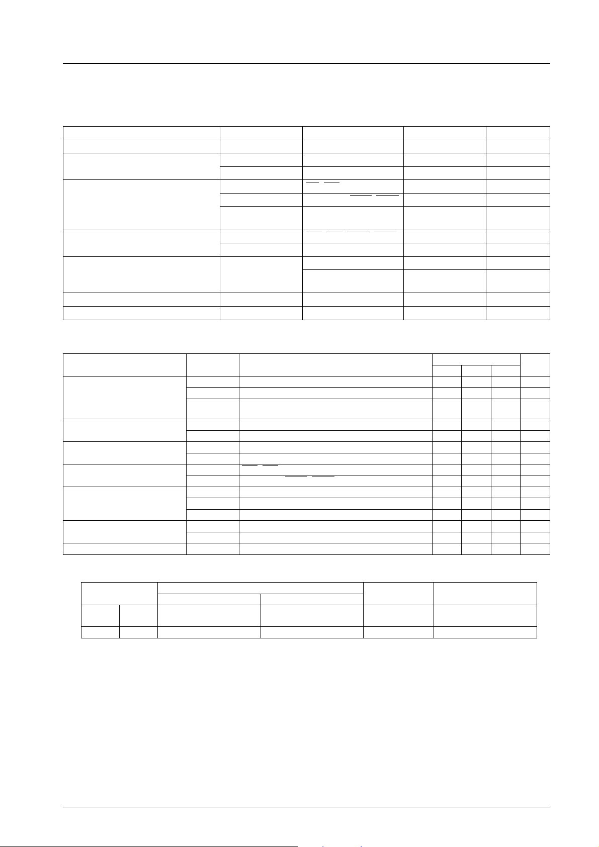
Specifications
Absolute Maximum Ratings at Ta = 25°C, VSS=0V
Parameter Symbol Conditions Ratings Unit
Maximum supply voltage V
Maximum input voltage
Maximum output voltage
Maximum output current
Allowable power dissipation Pd max
Operating temperature Topr –40 to +85 °C
Storage temperature Tstg –55 to +125 °C
Allowable Operating Ranges at Ta = –40 to +85°C, VSS=0V
max V
DD
V
max(1) CE, CL, DI, AIA, AIB –0.3 to +7.0 V
IN
V
max(2) XIN, PIA, PIB, TEST –0.3 to VDD+0.3 V
IN
max(1) LDI, LDB –0.3 to +7.0 V
V
O
V
max(2) AOA, AOB, OUTA, OUTB –0.3 to +15 V
O
V
max(3)
O
I
max(1) LDA, LDB, OUTA, OUTB 0to3 mA
O
I
max(2) AOA, AOB 0 to 6 mA
O
DD
PDA1, PDA2, PDB1,
PDB2, XOUT
–0.3 to +7.0 V
–0.3 to VDD+0.3 V
Ta% 85°C, LC7152 350 mW
Ta% 85°C, LC7152M,
7152NM, 7152KM
160 mW
Parameter Symbol Conditions
V
(1) V
Supply voltage
Input high-level voltage
Input low-level voltage
Output voltage
Input frequency
Input amplitude
Crystal oscillator frequency f
DD
V
(2) VDD:Serial data retention voltage, see Figure1, *1 1.5 V
DD
(3)
V
DD
V
(1) CE, CL, DI:VDD= 2.0 V 1.5 5.5 V
IH
V
(2) CE, CL, DI:VDD= 3.3 V 1.7 5.5 V
IH
V
(1) CE, CL, DI:VDD= 2.0 V 0 0.4 V
IL
V
(2) CE,CL,DI:VDD= 3.3 V 0 0.6 V
IL
V
(1) LDA, LDB 0 5.5 V
O
V
(2) AOA, AOB, OUTA, OUTB 013V
O
f
(1) XIN:Sine wave, capacitively coupled 1.0 13 MHz
IN
f
(2) PIA, PIB: Sine wave, capacitively coupled *2 1.5 55 MHz
IN
f
(3) PIA, PIB: Sine wave, capacitively coupled *3 55 80 MHz
IN
V
(1) XIN: Sine wave, capacitively coupled 200 600 mVrms
IN
V
(2) PIA, PIB: Sine wave, capacitively coupled *2,3 100 600 mVrms
IN
X’tal
DD
:Power-on reset voltage, tR^ 20 ms,
V
DD
see Figure1, *1
XIN, XOUT: CI % 50 Ω CL % 16 pF *4 4 10.24 11 MHz
Note *1 LC7152NM
FA/FB (serial data input frequency select bits)
[0] [1]
*2 f
*3 f
(2) 1.5 to 23 MHz 20 to 55 MHz 2.0 to 3.3 V
IN
(3) ————— 55 to 80 MHz 2.7 to 3.3 V LC7152KM
IN
*4 Cl is the crystal impedance and CL is the load capacitance.
Ratings
min typ max
Unit
2.0 3.3 V
0.05 V
V
DD
Device
LC7152, 7152M,
LC7152NM, 7152KM
No.3889-2/13
Page 3

LC7152, 7152M, 7152NM, 7152KM
Electrical Characteristics in the allowable operating ranges
Parameter Symbol Conditions
V
(1) PDA1, PDB1: IO= 1 mA VDD– 1.0 V
Output high-level voltage
Output low-level voltage
Output off-leakage current
Input high-level current
Input low-level current
Internal feedback resistance
OH
V
(2) PDA2, PDB2: IO= 2 mA VDD– 1.0 V
OH
V
(1) PDA1, PDB1: IO1 mA 1.0 V
OL
V
(2) PDA2, PDB2: IO= 2 mA 1.0 V
OL
V
(3) OUTA, OUTB: IO=1mA 1.0 V
OL
V
(4) LDA, LDB: IO=2mA 1.0 V
OL
V
(5) AOA, AOB: IO= 0.5 mA, AIA = AIB = 1.2 V 0.5 V
OL
V
(6) AOA, AOB: IO= 1 mA, AIA = AIB = 1.3 V 0.5 V
OL
I
(1) LDA. LDB: VO= 5.5 V 5.0 µA
OFF
I
(2) PDA1, PDB1, PDA2, PDB2: VO= 0/3.3 V 0.01 10.0 nA
OFF
I
(3) AOA, AOB, OUTA, OUTB: VO=13V 5.0 µA
OFF
(1) CE, CL, DI: VI= 5.5 V 5.0 µA
I
IH
I
(2) XIN: VI= 3.3 V, VDD= 3.3 V 2.0 6.5 µA
IH
I
(3) PIA, PIB: VI= 3.3 V, VDD= 3.3 V 3.5 10.0 µA
IH
I
(4) AIA, AIB: VI= 3.3 V 0.01 10.0 nA
IH
I
(5) TEST: VI= 3.3 V, VDD= 3.3 V 120 µA
IH
I
(1) CE, CL, DI: VI= 0 V 5.0 µA
IL
I
(2) XIN: VI=0V,VDD= 3.3 V 2.0 6.5 µA
IL
I
(3) PIA, PIB: VI=0V,VDD= 3.3 V 3.5 10.0 µA
IL
I
(4) AIA, AIB: VI= 0 V 0.01 10.0 nA
IL
I
(5) TEST: VI=0V,VDD= 3.3 V 5.0 µA
IL
R
(1) XIN: VDD= 3.3 V 1.0 MΩ
f
R
(2) PIA, PIB:VDD= 3.3 V 600 kΩ
f
Internal pull-down resistance Rd TEST: V
Input capacitance C
I
Supply current*1
Supply current*2
I
I
I
DD
DD
DD
DD
IN
XIN, PIA, PIB 2.5 pF
(1) VDD(= 2.0 V):fIN= 55 MHz 3.0 8.0 mA
(2) VDD(= 3.3 V):fIN= 55 MHz 7.0 14.0 mA
(4) VDD(= 2.0 V):fIN= 55 MHz 1.5 4.5 mA
(5) VDD(= 3.3 V):fIN= 55 MHz 3.9 8.0 mA
= 3.3 V 30 kΩ
DD
Ratings
min typ max
Unit
Note *1. Dual PLL operation (both PLL-A and PLL-B), SB= 0, XIN= 10.24 MHz (crystal), PIA and PIB input = 100mVrms at
f
, all other inputs at VSS, all other outputs open.
IN
*2. Standby mode: Single PLL operation (PLL-A operating and PLL-B stopped), SB = 1, XIN = 10.24 MHz (crystal), PIA
input = 100mVrms at f
, all other inputs at VSS, all other outputs open.
IN
Pin Assignment
No.3889-3/13
Page 4

Equivalent Block Diagram
LC7152, 7152M, 7152NM, 7152KM
Pin Functions
Symbol Pin No. Function
PIB 16 Side-B oscillator signal input
XIN 1
XOUT 24
PIA 14 Side-A oscillator signal output
V
DD
V
SS
CE 2
CL 3 Clock
DI 4 Data
TEST 8 IC Test
NC 7, 18 No connections
LDB
17 Power supply
15 Ground
Crystal oscillator
Serial data
input
5 Side-B unlock detection
Chip enable
Symbol Pin No. Function
PDB2 23 Sub charge pump
PDB1 22 Main charge pump
AIB 21
AOB 20
OUTB
LDA
PDA2 9 Sub charge pump
PDA1 10 Main charge pump
AIA 11
AOA 12
OUTA
19 General-purpose output port
6 Side-A unlock detection
13 General-purpose output port
Low-pass filter transistors
Low-pass filter transistors
No.3889-4/13
Page 5

Pin Description
LC7152, 7152M, 7152NM, 7152KM
Symbol Pin No. Function Description of function
PIA 14 Side-A local oscillator signal
PIB 16 Side-B local-oscillator signal
XIN
XOUT
PDA1
PDB1
PDA2
PDB2
LDA
LDB
AIA
AOA
AIB
OAB
OUTA
OUTB
input
input
1
Crystal oscillator
24
1022Side-A main charge pump
Side-B main charge pump
9
Side-A sub charge pump
23
Side-B sub charge pump
6
Side-A unlock detector output
5
Side-B unlock detector output
11
Side-A low-pass filter transistor
12
21
Side-B low-pass filter transistor
20
1319Side-A general purpose
output port
Side-B general purpose
output port
.
Side-A programmable divider. The input frequency ranges are as follows.
FA = [0] FA = [1] V
1.5 to 23 MHz 20 to 55 MHz 2.0 to 3.3 V
————— 55 to 80 MHz 2.7 to 3.3 V LC7152KM
FA: Serial data
.
Bits DA0 to DA15 determine the divider ratios
Divider ratio N = 272 to 65535
.
Side-B programmable divider
The input frequency ranges are the same as for PIA.
FB(→ FA): Determined by the serial data
.
Bits DB0 to DB15 determine the divider ratios
Divider ratio N= 272 to 65535
.
Serial data: Bit SB is the standby mode control bit
When SB = 1, standby mode is selected. In standby mode, side-B is
stopped, PIB is pulled down to V
When SB = 0, normal operation is selected.
.
Crystal oscillator connections (CI % 50 Ω,CL%16pF).
Note) When using a crystal other than as indicated above, its compatibility
with the crystal oscillator must be thoroughly studied.
.
These are PLL charge pump outputs that output the PLL phase error
signals. When the frequency generated by dividing the local oscillator signal
frequency by N is higher than the reference frequency, the charge pump
outputs a high-level signal for the phase error; when lower, the charge pump
outputs a low-level signal for the phase error.
If the two values match, these pins go to high-impedance.
.
fosc/N > fref or leading
.
fosc/N < fref or lagging
.
fosc/N = fref and coincidence
(*SB = [1] : PDB1 → High-Impedance)
.
PLL charge pump output; outputs PLL phase error signal only when the
unlock condition is detected.
.
The unlock detection threshold is set by serial data bits UL0 and UL1.
.
When a phase error that is shorter than the detection threshold occurs, this
signal goes to high impedance and the phase error signal for the main
charge pump is output.
.
The output pulse of the phase error signal has the same polarity as the main
charge pump.
.
Outputs the PLL lock/unlock status.
.
The unlock detection threshold for lock/unlock discrimination is set by serial
data bits UL0 and UL1.
.
The output phase error extension is set by serial data bits UE0 and UE1.
.
For details, refer to the description of the serial data.
.
SB=1:LDB→Open
.
MOS N-channel transistor for the PLL filter
.
The AOA and AOB output withstand voltage is 13V.
.
These latch the serial data bits OA and OB that are sent from the controller,
and then invert and output the data.
(OUTAcan also output XIN divided by two.
.
In the LC7152NM, OUTA and OUTB are open at the power-on reset.
→ Positive Pulse
→ Negative Pulse
→ High-Impedance
Locked: Open
Unlocked: Low
SS
DD
.
Device
LC7152, 7152M
LC7152NM, 7152KM
For more information on crystal oscillator : Nihon Dempa Kogyo Co., Ltd.
Continued on next page.
No.3889-5/13
Page 6

Continued from preceding page.
LC7152, 7152M, 7152NM, 7152KM
Symbol Pin No. Function Description of function
CE
*1
CL
*1
DI
*1
V
DD
V
SS
TEST 8 IC Test input
*1 The input ‘‘H’’ voltage and the input ‘‘L’’ voltage on the CE, CL, and DI pins are VIH= 1.5 to 5.5V and VIL= 0 to 0.4V
when V
to V
IH
2 Chip enable input
3 Clock input
4 Data input
1715Power supply
Ground
= 2.0V. When VDD= 3.3V, then VIH= 1.7 to 5.5V and VIL= 0 to 0.6V. (Voltage greater than VDDmay be applied
DD
.)
.
Set this pin high when inputting serial data to the LC7152.
.
Clock for data synchronization when inputting serial data to the LC7152.
.
Input for serial data being sent from the controller to the LC7152.
.
LC7152 power supply pin.
.
LC7152 test pin. (Normally VSSor open.)
.
However, divide-by-two XIN frequency is output from the pin OUTA by
applying the VDDlevel voltage after serial data transfer (T0 = T1 = T2 = 0).
Crystal oscillation frequency can be checked normally when the pin is left
open.
Serial Input Data (PLL Control data) format
Mode1: Latch-1 data (programmable divider data)
Mode data
Control data
No.3889-6/13
Page 7

LC7152, 7152M, 7152NM, 7152KM
Mode 2: Latch-2 data (reference divider and control data)
Mode data
Serial Data Transfer Timing
Control data
data = 0
Symbol Parameter 10.24 MHz crystal Other crystal frequencies
t
t
t
t
t
t
t
t
SU
HD
EL
ES
EH
CL
CH
LA
Data setup time At least 0.40 µs At least 4/f
Data hold time At least 0.40 µs At least 4/f
Enable low-level pulse
width
At least 0.40µs At least 4/f
Enable setup time At least 0.40 µs At least 4/f
Enable hold time At least 0.40 µs At least 4/f
Clock low-level pulse width At least 0.40 µs At least 4/f
Clock high-level pulse
width
At least 0.40 µs At least 4/f
Latch propagation delay Up to 0.40 µs Up to 4/f
X’tal
X’tal
X’tal
X’tal
X’tal
X’tal
X’tal
X’tal
Note Perform data transfer after the crystal oscillations normalize. Data transferred before normal
oscillations will not be recognized.
No.3889-7/13
Page 8

Description of Serial Data
LC7152, 7152M, 7152NM, 7152KM
No. Controller/Data Description Related Data
(1) Side-A
programmable
divider data: DA0
to DA15
(2) Side-B
programmable
divider data: DB0
to DB15
(3) Reference
frequency data: R0
to R13
(4) Output port data:
OA, OB
(5) Input frequency
range switching
data: FA, FB
(6) Standby mode data
:SB
(7) Unlock detection
data
: UL0, UL1
.
This data sets the side-A programmable divider number. This data is a
binary value in which DA0 is the LSB.
The range of divider values that can be set is 272 to 65,535.
NA = fVCO-A/fref
.
This data sets the side-B programmable divider number. This data is a
binary value in which DB0 is the LSB.
The range of divider values that can be set is 272 to 65,535.
NB = fVCO-B/fref
.
This data sets the reference divider number. This data is a binary value in
which R0 is the LSB.
The range of divider values that can be set is 8 to 16,383.
(Actual divider number) = (setting) x 2
(reference frequency: fref) = (f
.
This data determines the output on the general-purpose output port.
OA → OUTA
OB → OUTB
.
Data 0: open; Data 1: low
.
During the power-on reset in the LC7152NM, OA and OB are both ‘‘0’’.
.
This data switches the input frequency range for the PIA and PIB pins.
(FA → PIA, FB → PIB)
Data
[0] 1.5 to 23 MHz
[1] 20 to 55 MHz
.
In the case of the LC7152KM: Data 1: 55 to 80 MHz (VDD= 2.7 V to 3.3 V)
.
This data puts the PLL in standby mode.
.
SB = 1: standby mode (LDB pin: open)
→ Single PLL operation: Side-A operating, side-B stopped
.
SB = 0: standby mode off
.
.
→ Dual PLL operation: Side-A operating, side-B operating
During the power-on reset in the LC7152NM, SB is ‘‘1’’.
This is the phase error detection threshold data that is used for PLL
lock/unlock discrimination. If the threshold shown in the table is exceeded,
the unlocked state is detected.
UL0 UL1
00 0 ←←←←←
10 ±4/f
01±16/f
11±64/f
Phase error
detector
threshold
X’tal
Supply voltage (V
4.0 7.2 8.0 10.24 12.8
±1.00 ±0.55 ±0.50 ±0.39 ±0.31
X’tal
X’tal
±4.00 ±2.22 ±2.00 ±1.56 ±1.20
±16.00 ±8.88 ±8.00 ±6.25 ±5.00
: XIN)/(actual divider number)
X’tal
)
2.0 to 3.3 V
DD
XIN : fXIN [MHz] example
unit : µs
R0 to R13
R0 to R13
UL0 Ul1 UE0 UE1
DA0 to DA15
DB0 to DB15
: UE0, UE1
(Note) Note that if the data changes in lock state, the PLL will be unlocked
temporarily.
.
The detected phase error (øE) signal can be extended by a certain amount
of time and output on the LDA and LDB pins. This data determines the
length of this extension. However, when UL0 = UL1 = 0, the phase error is
not extended, and is output directly.
UE0 UE1
00 4×(1/fref) 4.0* 0.8 0.32
10 8×(1/fref) 8.0 1.6 0.64
0132×(1/fref) 32.0 6.4* 2.56
1164×(1/fref) 64.0 12.8 5.12*
Reference
frequency
fref
Reference frequency :
fref [kHz] example
1 kHz 5 kHz 12.5 kHz
(*standard value)
unit : ms
Continued on next page.
No.3889-8/13
Page 9

Continued from preceding page.
LC7152, 7152M, 7152NM, 7152KM
No. Controller/Data Description Related Data
(8) Dead zone control
data: DZ
(9) IC test data: T0,
T1, T2
.
This data controls the phase comparator dead zone.
(DZA < DZB)
DZ Mode
0 DZA
1 DZB
.
This is the IC test mode switching data. The user does not need to be
concerned about this data.
Assume that T0 = T1 = T2 = 0.
Normally, the test pins must be either at V
or left open.
SS
Power-on Reset supply voltage
Figure 1. Power-on reset supply voltage (LC7152NM only)
.
Power-on reset is performed when the supply voltage VDDexceeds 2.0 V by power application after the VDDhas once fallen
under 0.05 V and kept the level for at least 20ms.
.
Latch data is retained when the VDDis 1.5 V, where power-on reset is not performed.
No.3889-9/13
Page 10

LC7152, 7152M, 7152NM, 7152KM
Sample Application Circuit (FCC: 10 ch 46/49 MHz cordless telephone)
No.3889-10/13
Page 11

LC7152, 7152M, 7152NM, 7152KM
Example: FCC 1-channel 46/49 MHz cordless telephone base station (See diagram in the preceding page.)
for fref: 5 kHz, RX VCO: 38.975 MHz, TX VCO: 46.610 MHz
Programmable Divider Data
(1)
(2)
(3) Reference frequency data
(4) Output port data
General-purpose output port: Open (OA = 0, OB = 0)
(5) Input frequency range select bits
FA=FB=1
(6) Standby mode
During standby (SB = 1)
(7) Unlock detector output
Extends the phase error signal by 6.4ms if a phase error of ±6.25 µs or more is generated.
:UL0=UL1=1
:UE0=0,UE1=1
(8) Dead-zone control data
DZA mode : DZ = 0
(9) LSI test data: T0 = T1= T2 = 0
(1) Mode 1: Latch-1 data
(2) Mode 2: Latch-2 data
: data = 0
No.3889-11/13
Page 12

LC7152, 7152M, 7152NM, 7152KM
Dual Charge Pump Descriptions
(Unlock detector output)
(Secondary charge pump output)
(Main charge pump output)
(Low-pass filter output)
If an unlock state is detected at channel switch, the sub-charge pump operates, R1M/R1S becomes R1, low-pass filter’s time
constant is reduced, and the lockup accelerates.
When the circuit is locked, side-band characteristics and modulation characteristics are improved by making the sub-charge pump
off, i.e., floating, R1M to be R1, and increasing low-pass filter’s time constant.
Device Comparison
Operating frequency
Device
1.5 to 23 MHz 20 to 55 MHz 55 to 80 MHz
LC7152 Yes Yes No No DIP24S
LC7152M Yes Yes No No MFP24S
LC7152NM Yes Yes No Yes MFP24S
LC7152KM Yes Yes
(V
= 2.7 to 3.3 V)
DD
Yes
Power-on reset
circuit
No MFP24S
PackageFA/FB = 0 FA/FB = 1
No.3889-12/13
Page 13

LC7152, 7152M, 7152NM, 7152KM
Specifications of any and all SANYO products described or contained herein stipulate the performance,
characteristics, and functions of the described products in the independent state, and are not guarantees
of the performance, characteristics, and functions of the described products as mounted in the customer’s
products or equipment. To verify symptoms and states that cannot be evaluated in an independent device,
the customer should always evaluate and test devices mounted in the customer’s products or equipment.
SANYO Electric Co., Ltd. strives to supply high-quality high-reliability products. However, any and all
semiconductor products fail with some probability. It is possible that these probabilistic failures could
give rise to accidents or events that could endanger human lives, that could give rise to smoke or fire,
or that could cause damage to other property. When designing equipment, adopt safety measures so
that these kinds of accidents or events cannot occur. Such measures include but are not limited to protective
circuits and error prevention circuits for safe design, redundant design, and structural design.
In the event that any or all SANYO products(including technical data,services) described or
contained herein are controlled under any of applicable local export control laws and regulations,
such products must not be exported without obtaining the export license from the authorities
concerned in accordance with the above law.
No part of this publication may be reproduced or transmitted in any form or by any means, electronic or
mechanical, including photocopying and recording, or any information storage or retrieval system,
or otherwise, without the prior written permission of SANYO Electric Co. , Ltd.
Any and all information described or contained herein are subject to change without notice due to
product/technology improvement, etc. When designing equipment, refer to the “Delivery Specification”
for the SANYO product that you intend to use.
Information (including circuit diagrams and circuit parameters) herein is for example only ; it is not
guaranteed for volume production. SANYO believes information herein is accurate and reliable, but
no guarantees are made or implied regarding its use or any infringements of intellectual property rights
or other rights of third parties.
This catalog provides information as of June, 1999. Specifications and information herein are subject to
change without notice.
PS No.3889-13/13
 Loading...