

Page 1
Any and all SANYO products described or contained herein do not have specifications that can handle
applications that require extremely high levels of reliability, such as life-support systems, aircraft’s
control systems, or other applications whose failure can be reasonably expected to result in serious
physical and/or material damage. Consult with your SANYO representative nearest you before using
any SANYO products described or contained herein in such applications.
SANYO assumes no responsibility for equipment failures that result from using products at values that
exceed, even momentarily, rated values (such as maximum ratings, operating condition ranges,or other
parameters) listed in products specifications of any and all SANYO products described or contained
herein.
CMOS IC
C MOS Si Gate IC
Meeting FCC 10-Channel Standard
PLL for Cordless Telephone
Ordering number:ENN2365B
LC7151
SANYO Electric Co.,Ltd. Semiconductor Company
TOKYO OFFICE Tokyo Bldg., 1-10, 1 Chome, Ueno, Taito-ku, TOKYO, 110-8534 JAPAN
Functions
• On-chip PLL for transmission/reception.
• On-chip digital unlock detector.
(only PLL for transmission)
• 5.0kHz/4.4kHz output pins for guard tone.
• Standby function.
• Pull-down resistance at CH select pins (D1 to D4).
LC7150 : With (for mechanical SW)
LC7151 : Without (for µCOM)
Specifications
Absolute Maximum Ratings at Ta = 25˚C, VSS=0V
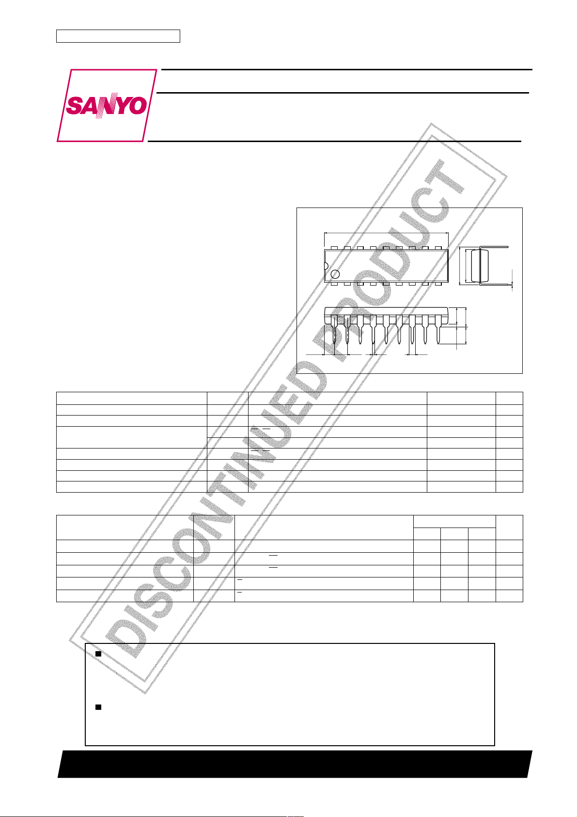
Package Dimensions
unit:mm
3007B-DIP18
[LC7151]
24.0
18
1
(1.84)
retemaraPlobmySsnoitidnoCsgnitaRtinU
egatlovylppusmumixaMV
egatlovtupnimumixaMV
egatlovtuptuomumixaM
tnerructuptuOI
noitapissidrewopelbawollAxamdPaT ≤ 57°C 053Wm
erutarepmetgnitarepOrpoT 57+ot03–
erutarepmetegarotSgtsT 521+ot04–
xam 5.6+ot3.0–V
DD
xamsniptupnillAVot3.0–
I
V
xamFFOtuptuo2F,1F 5.6+ot3.0–V
1O
V
xamVnahtrehtosniptuptuO
2O
TUO
TDL,2F,1F 0.3ot0Am
2.54
1O
1.20.5
10
9
6.4
7.62
(3.25)
3.85max
3.3
0.51min
SANYO : DIP18
3.0+V
DD
Vot3.0–
3.0+V
DD
0.25
˚C
˚C
Allowable Operating Conditions at Ta = 25˚C, VSS=0V
retemaraPlobmySsnoitidnoC
egatlovylppuSV
egatlovlevel-hgihtupnIV
egatlovlevel-woltupnIV
egatlovlevel-hgihtupnIV
egatlovlevel-woltupnIV
DD
1HI
1LI
2HI
2LI
BS,4Dot1D
BS,4Dot1D0
B/R
B/R0
51501TN (KT)/21593JN/8237KI/D026KI, TS No.2365–1/5
sgnitaR
nimpytxam
0.35.5V
V7.0
DD
V9.0
DD
V
DD
V3.0
DD
V
DD
V1.0
DD
Continued on next page.
tinU
V
V
V
V
Page 2
LC7151
Continued from preceding page.
retemaraPlobmySsnoitidnoC
f
1NI
ycneuqerftupnI
edutilpmatupnI
f
2NI
f
3NI
V
1NI
V
2NI
V
3NI
Electrical Characteristics at Ta = 25˚C, under Allowable Operating Conditions
retemaraPlobmySsnoitidnoC
tnerruclevel-hgihtupnII
tnerruclevel-woltupnII
tnerruclevel-hgihtupnII
tnerruclevel-woltupnII
tnerruclevel-hgihtupnII
tnerruclevel-woltupnII
ecnatsiseRkcabdeeF
egatlovlevel-hgihtuptuOV
egatlovlevel-woltuptuOV
tnerrucegakaelFFOtuptuOI
egatlovlevel-hgihtuptuOV
tnerrucegakaelFFOtuptuOI
egatlovlevel-woltuptuOV
tnerrucegakaelFFOtuptuOI
niardtnerruC
1HI
1LI
2HI
2LI
3HI
3LI
R
1f
R
2f
1HO
1LO
1ffo
2HO
2ffo
2LO
3ffo
I
1DD
I
2DD
I
3DD
I
4DD
I
5DD
I
6DD
(Note) Power VDD–VSS : Insert a capacitor of 2000pF or greater.
V;TIP
NI
V;RIP
NI
V;NIX
NI
f;TIP
NI
f;RIP
NI
f;NIX
NI
V;NIX
IV=DD
V;NIX
IV=SS
V;NIX
DD
I;TDL
O
I;2F,1F
O
V)3C(
DD
V)3C(
DD
V)3C(
DD
V)2C(
DD
V)2C(
DD
V)2C(
DD
(C3) : XIN=10.24MHz, Xtal connected
PIT=27MHz 150mVrms
PIR=42MHz 150mVrms
R/B=VDD, SB=VDD, other pin open
(C2) : XIN=10.24MHz, Xtal connected
PIR=42MHz, 150mVrms
R/B=VDD, SB=VSS, other pin open
smrV51.0=0172zHM
smrV51.0=0324zHM
smrV3.0=0.542.010.11zHM
zHM72=51.0
zHM24=51.0
zHM11=3.0
V;RIP,TIP
IV=DD
V;RIP,TIP
IV=SS
V;4Dot1D,B/R,BS
IV=DD
V;4Dot1D,B/R,BS
IV=SS
V3.4=0.1MΩ
V;RIP,TIP
V3.4=5.0MΩ
DD
I;RDP,TDP
Am5.0=
O
I;RDP,TDP
Am5.0=0.1V
O
V;RDP,TDP
OV=DDV/SS
Am1=
VFFOtuptuo;TDL
OV=SS
Am1=0.1V
VFFOtuptuo;2F,1F
V5.5=0.5Aµ
O
V0.3=4Am
V5.4=7Am
V5.5=31Am
V0.3=3Am
V5.4=5Am
V5.5=01Am
nimpytxam
nimpytxam
VDD0.1–
VDD0.1–
sgnitaR
V3.0
DD
V3.0
DD
V3.0
DD
sgnitaR
02Aµ
02Aµ
04Aµ
04Aµ
01Aµ
01Aµ
10.00.1An
0.5Aµ
tinU
smrV
smrV
smrV
tinU
V
V
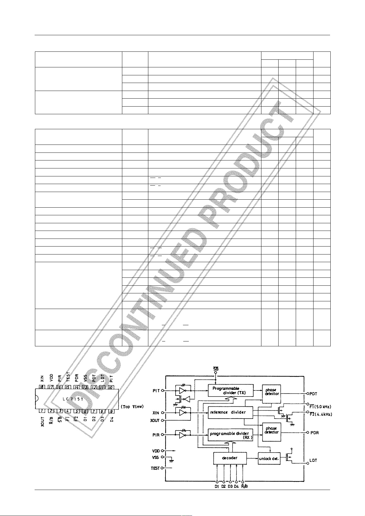
Pin Assignment Equivalent Circuit Block Diagram
No.2365–2/5
Page 3

Sample Application Circuit
LC7151
Pin Description
F1 : 5.0kHz output. When not used, connect to V
SS
.
F2 : 4.4kHz output (10.24MHz÷2304). When not used, connect to VSS.
VDD, VSS : Power supply.
XIN, XOUT : Crystal resonator (10.24MHz).
D1 to D4 : Channel select pin.
R/B : Base unit/remore unit select pin.
R/B= “0” (V
R/B= “1” (V
)............ Remote unit
SS
)........... Base unit
DD
SB : Used to stop the TX PLL at the standby mode to minimize current drain.
SB= “0” (VSS) ............. The charge pump enters a high-impedance mode.
Standby mode. Only the RX PLL is operated.
SB= “1” (V
) ............ The TX, RX PLL are operated.
DD
PIT : TX programmable divider input pin.
PIR : RX programmable divider input pin.
PDT : TX charge pump output pin.
PDR : RX charge pump output pin.
TEST : IC test input pin. Connected to V
SS
.
LDT : TX PLL unlock signal output pin.
No.2365–3/5
Page 4

LC7151
When the phase difference becomes tD (=6.25µs) or more, 5.6ms output pulse is delivered at the LDT pin.
Table of Frequency Division
TUPNI
C
H
f
4D3D2D1D
0001
0010
0011
0100
0101
0110
0111
1000
1001
1010
1011
1100
1101
1110
1111
0000
XT
)zHM(
1
2
3
4
5
6
7
8
9
01
01
01
01
01
01
01
076.94
548.94
068.94
077.94
578.94
038.94
098.94
039.94
099.94
079.94
079.94
079.94
079.94
079.94
079.94
079.94
)zHk5.2=ferf(XT)zHk5=ferf(XR)zHk5.2=ferf(XT)zHk5=ferf(XR
f
OCV
)zHM(
0538.42
5229.42
0339.42
0588.42
5739.42
0519.42
0549.42
0569.42
0599.42
0589.42
0589.42
0589.42
0589.42
0589.42
0589.42
0589.42
)'0'=B/R(ETOMER)'1'=B/R(ESAB
f
OCV
N
4399
9699
2799
4599
5799
6699
8799
6899
8999
4999
4999
4999
4999
4999
4999
4999
N
)zHM(
3817
519.53
7817
539.53
5917
579.53
3027
510.63
7027
530.63
5127
570.63
7227
531.63
5327
571.63
7427
532.63
5527
572.63
5527
572.63
5527
572.63
5527
572.63
5527
572.63
5527
572.63
5527
572.63
f
f
XT
OCV
)zHM(
016.64
036.64
076.64
017.64
037.64
077.64
038.64
078.64
039.64
079.64
079.64
079.64
079.64
079.64
079.64
079.64
)zHM(
503.32
513.32
533.32
553.32
563.32
583.32
514.32
534.32
564.32
584.32
584.32
584.32
584.32
584.32
584.32
584.32
f
OCV
N
2239
6239
4339
2439
6439
4539
6639
4739
6839
4939
4939
4939
4939
4939
4939
4939
N
)zHM(
5977
579.83
0387
051.93
3387
561.93
5187
570.93
6387
081.93
7287
531.93
9387
591.93
7487
532.93
9587
592.93
5587
572.93
5587
572.93
5587
572.93
5587
572.93
5587
572.93
5587
572.93
5587
572.93
No.2365–4/5
Page 5

LC7151
Specifications of any and all SANYO products described or contained herein stipulate the performance,
characteristics, and functions of the described products in the independent state, and are not guarantees
of the performance, characteristics, and functions of the described products as mounted in the customer's
products or equipment. To verify symptoms and states that cannot be evaluated in an independent device,
the customer should always evaluate and test devices mounted in the customer's products or equipment.
SANYO Electric Co., Ltd. strives to supply high-quality high-reliability products. However, any and all
semiconductor products fail with some probability. It is possible that these probabilistic failures could
give rise to accidents or events that could endanger human lives, that could give rise to smoke or fire,
or that could cause damage to other property. When designing equipment, adopt safety measures so
that these kinds of accidents or events cannot occur. Such measures include but are not limited to protective
circuits and error prevention circuits for safe design, redundant design, and structural design.
In the event that any or all SANYO products(including technical data,services) described or
contained herein are controlled under any of applicable local export control laws and regulations,
such products must not be exported without obtaining the export license from the authorities
concerned in accordance with the above law.
No part of this publication may be reproduced or transmitted in any form or by any means, electronic or
mechanical, including photocopying and recording, or any information storage or retrieval system,
or otherwise, without the prior written permission of SANYO Electric Co. , Ltd.
Any and all information described or contained herein are subject to change without notice due to
product/technology improvement, etc. When designing equipment, refer to the "Delivery Specification"
for the SANYO product that you intend to use.
Information (including circuit diagrams and circuit parameters) herein is for example only ; it is not
guaranteed for volume production. SANYO believes information herein is accurate and reliable, but
no guarantees are made or implied regarding its use or any infringements of intellectual property rights
or other rights of third parties.
This catalog provides information as of May, 2001. Specifications and information herein are subject to
change without notice.
PS No.2365–5/5
 Loading...