

Page 1

Any and all SANYO products described or contained herein do not have specifications that can handle
applications that require extremely high levels of reliability, such as life-support systems, aircraft’s
control systems, or other applications whose failure can be reasonably expected to result in serious
physical and/or material damage. Consult with your SANYO representative nearest you before using
any SANYO products described or contained herein in such applications.
SANYO assumes no responsibility for equipment failures that result from using products at values that
exceed, even momentarily, rated values (such as maximum ratings, operating condition ranges,or other
parameters) listed in products specifications of any and all SANYO products described or contained
herein.
CMOS IC
Synchronous Error Correction IC
for RDS Applications
Ordering number:ENN4789
LC7074, 7074M
SANYO Electric Co.,Ltd. Semiconductor Company
TOKYO OFFICE Tokyo Bldg., 1-10, 1 Chome, Ueno, Taito-ku, TOKYO, 110-8534 JAPAN
Overview
The LC7074 and the LC7074M are ICs for the RDS (radio
data system) implemented by the EBU (European Broadcasting Union) and the RDBS (radio broadcast data system) implemented by the NRSC (National Radio System
Committee) in the USA.
RDS and RBDS are standards that allow data to be broadcast multiplexed with other FM broadcasts. When combined
with an IC in the LA2230 series, the LC7074/M synchronizes with data multiplexed in an FM broadcast and detects and corrects errors in that data. The synchronized data
is output as a serial signal which can then be decoded and
processed on the system control microprocessor.
Functions
• Group synchronization.
RDS group synchronization.
MMBS/RDS group synchronization.
• Error detection and correction.
• Error detection function enable/disable selection.
• Serial data output.
• Serial data clock polarity selection.
• Data block start signal output.
Features
• System that decode, synchronize and detect and correct
errors can easily be constructed by combining the
LC7074/M with an LA2230 series product.
• Reduces overhead in the microprocessor that decodes and
processes the RDS or MMBS/RDS data.
Product-Package Relationship
.oNtcudorPegakcaP
4707CL81PID
M4707CL81PFM
Package Dimensions
unit:mm
3007B-DIP18
[LC7074]
24.0
(1.84)
18
1
2.54
10
9
1.20.5
unit:mm
3095-MFP18
[LC7074M]
18
1
12.6
0.35
1.27
10
9
1.5
0.1
1.22
6.4
7.62
(3.25)
3.85max
3.3
0.51min
SANYO : DIP18
5.4
0.15
1.8max
7.6
6.35
0.625
SANYO : MFP18
0.25
80101TN (KT)/12094JN B8-0839 · 0840 No.4789–1/17
Page 2

Pin Assignment
LC7074, 7074M
The LC7070 Series
This section describes the differences between the different products in the LC7070 series
Usage Notes
This basic functions, including the pin functions and I/O timing, are identical in all products in the series. However,
some pin circuits and function operation details differ.
• LC7070NM…While the LC7074M is pin compatible with this product, the circuit type of the three output pins differs
as shown in table, Package and Output Driver Type Comparison. These products can be interchanged
to match the output interface. However, since the data output method following synchronization
detection differs as shown in table, Comparison of Functional Differences, care is required in writing
programs that receive, decode and process the output data for the control microprocessor.
• LC7070N……While the LC7074 is pin compatible with this product, the circuit type of the three output pins differs as
shown in table, Package and Output Driver Type Comparison. These products can be interchanged to
match the output interface. However, since the data output method following synchronization detection
differs as shown in table, Comparison of Functional Differences, care is required in writing programs
that receive, decode and process the output data for the control microprocessor.
• LC7071NM…The LC7074M is pin compatible with this product, and the pin circuit types, pin functions, and signal
timings are identical. In principle, these products are interchangeable. However, since the data output
method following synchronization detection differs as shown in table, Comparison of Functional
Differences, care is required in writing programs that receive, decode and process the output data for
the control microprocessor.
• LC7073………The LC7074 is pin compatible with this product, and the pin circuit types, pin functions, and signal
timings are identical. Furthermore, the synchronization detection method and the post-synchronization
data output method are also identical. In principle, these products are interchangeable. However, since
these products handle the block offset words E and F differently, and also handle MMBS/RDS data
differently as shown in table, Comparison of Functional Differences, care is required in writing
programs that receive, decode and process the output data for the control microprocessor.
• LC7073M……The LC7074M is pin compatible with this product, and the pin circuit types, pin functions, and signal
timings are identical. Furthermore, the synchronization detection method and the post-synchronization
data output method are also identical. In principle, these products are interchangeable. However, since
these products handle the block offset words E and F differently, and also handle MMBS/RDS data
differently as shown in table, Comparison of Functional Differences, care is required in writing
programs that receive, decode and process the output data for the control microprocessor.
No.4789–2/17
Page 3

LC7074, 7074M
Package and Output Driver Type Comparison
.oNtcudorPegakcaP*ecnereffidepytrevirdtuptuOnoitcnuF
N0707CL81PID
MN1707CL81PFM)epytSOMC(rotsisnartSOMpu-lluP
3707CL81PID
M3707CL81PFM
4707CL81PID
M4707CL81PFM
Note: *Only applies to the three pins DATA START, DATA OUT and CLOCK OUT.
Comparison of Functional Differences
metI
EdrowtesffO
FdrowtesffO
atadorezllA
-tsoP
tuptuo
noitcerrocrorrE
)Etesffootgnidnopserroc(
ataddnuopmocSDR/SBMM
.detpurretni
dohtemnoitcetednoitazinorhcnyS
.redro
atadnoitcetednoitazinorhcnys
dohtemnoitanimretedtuo-lluP
epytniardnepO
)epytSOMC(rotsisnartSOMpu-lluP
)epytSOMC(rotsisnartSOMpu-lluP
N0707CL
MN0707CL
MN1707CL
.demrofrepsinoitarepo
sdrowtesffoebotnekateraesehT
noitazinorhcnyspuorgadna
.demrofrepsinoitareponoitceted
tesffonaebotnekatsiatadorezllA
tesffona,ylgnidroccA.kcolbEdrow
noitazinorhcnyskcolbEdrow
SDRnamorfnoitisnartehtroF
puorgSBMMnaot)DCBA(puorg
,noitisnartesreverehtro)EEEE(
tuo-llupehtebotnekateraeseht
.secneuqesnoitazinorhcnyserdna
nacsrorreatad,snoitisnartgniruD
ebnactuptuoataddnarucco
nehwdeveihcasinoitazinorhcnyS
21fotuoevifnisdrowtesffoeht
tcerrocehtnidetcetederaskcolb
morfatadehthtiwstratstuptuoataD
Adrowtesffoeht(kcolbtsrifeht
ehtgniwollofpuorgehtni)kcolb
noitazinorhcnyshcihwrofpuorg
.detelpmocsawnoitceted
.demrofrep
.ecneuqes
3707CL
M3707CL
.detcetedera
.kcolbEdrowtesffo
eseht,tupnisiatadorezllafI
tuo-llupehtretnednaatad
tonodstcudorpesehtecniS
dnatuo-llupehttaeper
.puorgemasehtmorf
.puorgemasehtmorf
snoitcnuflacitnedIMN0707CL81PFM
fonosirapmoC,elbateeS
.secnereffiDlanoitcnuF
fonosirapmoC,elbateeS
.secnereffiDlanoitcnuF
4707CL
M4707CL
.sdrowtesffosaneestoneraesehT
Ddna'C,C,B,AsdrowtesffoylnO
nagniebsaneestonsiatadorezllA
otnekatsiatadorezlla,rehtaR
dna,tupnionsierehttahtnaem
tonsinoitcetednoitazinorhcnys
sahtupniatadtahtedicedstcudorp
gnittuptuopotsyehtdna,deppots
Edrowtesffonanoezinorhcnys
sipuorgSDRnaemithcae,kcolb
yeht,puorgSBMMnanidetresni
.secneuqesnoitazinorhcnyser
.redrotcerrocehtnidetcetederaskcolb
.detcetedtonerewskcolbevitucesnoceromroevifmorfsdrowtesffoehtnehW
.detcetedera
EdnaD,'C,C,B,AsdrowtesffO
.detcetedtonsiFdrowtesffO
tesffonasaneessiatadorezllA
tesffona,ylgnidroccA.kcolbEdrow
noitazinorhcnyskcolbEdrow
.demrofrepsinoitarepo
tuptuoyltcerrocsiatadSDR/SBMM
.srorreondnatuo-lluponhtiw
eerhtfotuoowtnisdrowtesffoehtnehwdeveihcasinoitazinorhcnyS
,kcolbAdrowtesffonahtiwsetelpmocnoitcetednoitazinorhcnysnehW
)kcolbBdrowtesffoeht(kcolbdnocesehtniatadehthtiwstratstuptuo
DroC,BdrowtesffonahtiwsetelpmocnoitcetednoitazinorhcnysnehW
)kcolbAdrowtesffoeht(kcolbtsrifehtniatadehthtiwstratstuptuo,kcolb
.sselrostib5fosecnatsidrofdetcerrocerastibrorreevifotpu,delbanesinoitcerrocrorreerehwsedomnI
No.4789–3/17
Page 4

Block Diagram
LC7074, 7074M
No.4789–4/17
Page 5
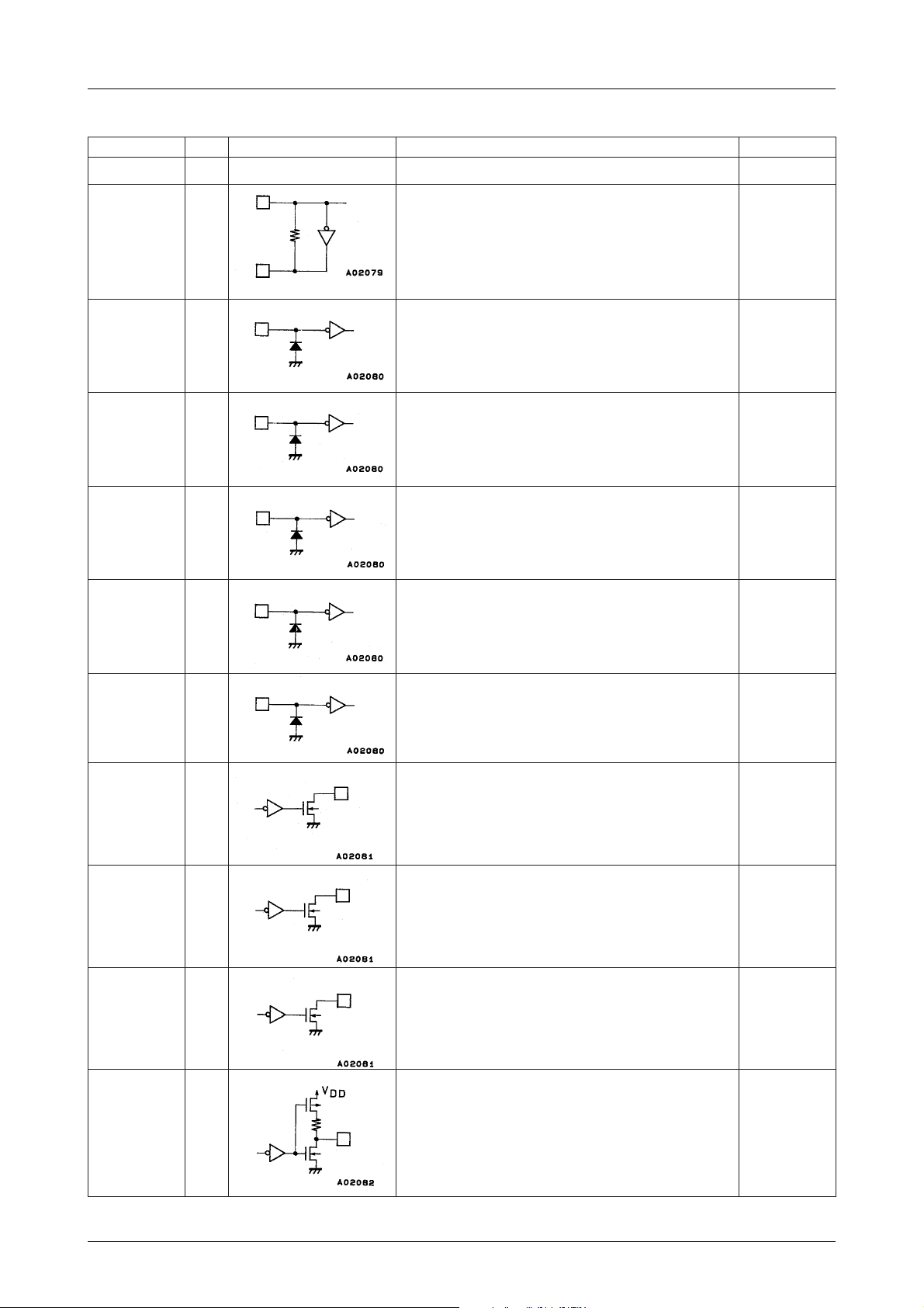
Pin Functions
niPO/ItiucrictnelaviuqelanretnInoitcnuFtesertaeulaV
VDDV,
V
1SS
V,
2SS
3SS
LC7074, 7074M
ylppusrewoP
1CSO
2CSO
NIKCOLCI
NIATADI
LES.RROCI
LES.DE.LCI
I
O
rotallicsokcolC
tupnikcolcnoitaludomedSDR
.CI
tupniatadnoitaludomedSDR
tupninoitcelesnoitcerrocrorrE
SDRehtnisrorrestcerrocCIehtrehtehwstcelesnipsihT
.ataddetaludomed
*demrofrepnoitcerrocoN:0=tupnI
demrofrepnoitcerrocrorrE:1=tupnI
.sselrostib5fosecnatsidrofdetcerroc
tupninoitcelesytiraloptuptuokcolcatadlaireS
.snipesehttaroticapacdnarotallicsocimareclanretxeehttcennoC
noitaludomedseires0322ALehtmorftuptuokcolcehtottcennoC
.CInoitaludomedseires0322ALehtmorftuptuoatadehtottcennoC
erastibrorreevifotpu,delbanesinoitcerrocrorreerehwsedomnI
tuptuoehtfoegdegnisirehtnodilavsituptuoatadlaireS:0=tupnI
).kcolcehtfoegdegnillafehtnosegnahctuptuoataD(.kcolc
tuptuoehtfoegdegnillafehtnodilavsituptuoatadlaireS:1=tupnI
).kcolcehtfoegdegnisirehtnosegnahctuptuoataD(.kcolc
LORTNOC.S.DI
EVIECERO
NOITCERROCO
RORREO
TRATSATADO
tupnilortnoclangistratsatadkcolB
tuptuossergorpninoitpeceratadSDR
.semitrehto
tuptuoniardnepO
tuptuonoitareponoitcerrocrorrE
.delbasidsinoitcerrocnehw)ecnadepmi
tuptuoniardnepO
tuptuororrE
tuptuoniardnepO
langistratsatadkcolbtuptuoatadlaireS
tuptuo)SOMC(rotsisnartSOMpu-lluP
.skcolbllaroflangisTRATSATADehttuptuO:0=tupnI
.tupniLOTNOC.S.DehtybdellortnocsiepyttuptuoehT
.kcolbdnocesehtylnoroflangisTRATSATADehttuptuO:1=tupnI
gniwolloftuptuogniebsiatadlaireselihwlevelwolastuptuO
llatalevelhgihastuptuO.noitcetednoitazinorhcnysfonoitelpmoc
rorreneebsahatadtuptuoatadlairesehtnehwlevelwolastuptuO
hgih(levelhgihastuptuO.detcerrocebtondluocro,detcerroc
dnaatadtupniehtnisrorreerewerehtnehwlevelwolastuptuO
hgih(levelhgihastuptuO.detcerrocebtondluocsrorreesoht
.detcerrocerewsrorreehtrosrorreonerewerehtnehw)ecnadepmi
levelhgiH
)ecnadepmihgih(
levelhgiH
)ecnadepmihgih(
levelhgiH
)ecnadepmihgih(
levelhgiH
Continued on next page.
No.4789–5/17
Page 6

Continued from preceding page.
niPO/ItiucrictnelaviuqelanretnInoitcnuFtesertaeulaV
LC7074, 7074M
TUOATADO
TUOKCOLCO
tupniteseR
SERI
.tupniepytttimhcS
tuptuoatadtuptuoatadlaireS
tuptuo)SOMC(rotsisnartSOMpu-lluP
tuptuokcolctuptuoatadlaireS
tuptuo)SOMC(rotsisnartSOMpu-lluP
teserotselcyckcolc4tsaeltafohtgnelahtiwesluplevelwolatupnI
,desusirotallicsozHM4anehwtahtetoN.noitarepoCItratserdna
.sµ1siselcyckcolcruof,sµ52.0sielcyckcolcelgnisaecnis
rotsiserpu-llupni-tliuB
levelhgiH
levelhgiH
Note: *0: Low level input
1: High level input
Specifications
Electrical Characteristics at Ta = 25˚C, V
retemaraPlobmySsnoitidnoCsgnitaRtinU
egatlovylppuSV
egatlovtuptuO
egatlovtupnI
tnerructuptuO
noitapissidrewopelbawollAdPxam
erutarepmetgnitarepOrpoT –58+ot04
erutarepmetegarotSgtsT –521+ot55
Note: *When driving the oscillator with the recommended constants shown in figure 1, values up to the oscillation
amplitude that occurs are allowed.
DD
V
V
V
V
I
I
, V
, V
SS1
SS2
xamV
DD
1O
2O
1I
2I
1O
2O
I
O
niprep
DIP package product: Ta=–40 to +85˚C
MFP package product: Ta=–40 to +85˚C
= 0V
SS3
*:1CSO,SER–Vot3.0
LORTNOC.S.D
nipreptnerruc
–0.7+ot3.0V
TUOKCOLC,TUOATAD,TRATSATAD,2CSO–Vot3.0
RORRE,NOITCERROC,EVIECER–51+ot3.0V
,LES.DE.LC,LES.RROC,NIATAD,NIKCOLC
tnerructuptuoehT:RORRE,NOITCERROC,EVIECER
tuptuoehT:TUOKCOLC,TUOATAD,TRATSATAD
eulavlatoT:sniptuptuollA–09+ot41Am
–51+ot3.0V
3.0+V
DD
3.0+V
DD
02Am
–02+ot2Am
052otpUWm
051otpUWm
˚C
˚C
Allowable Operating Ranges at Ta = –40 to +85˚C, V
retemaraPlobmySsnoitidnoC
egatlovylppusgnitarepOV
egatlovlevel-hgihtupnI
egatlovlevel-woltupnI
eetnaraugrotallicsocimareC 1erugifeeS:2CSO,1CSO
V
V
V
V
V
DD
DD
1HI
SERV8.0
2HI
1LI
SERV
2LI
SS1
LORTNOC.S.D
LORTNOC.S.D
, V
SS2
, V
= 0V, VDD = 4.5 to 6.0V
SS3
nimpytxam
,LES.DE.LC.LES.RROC,NIATAD,NIKCOLC
V7.0
DD
,LES.DE.LC.LES.RROC,NIATAD,NIKCOLC
DD
V
SS
SS
sgnitaR
5.40.6V
V
V3.0
V52.0
.elbatstnatsnoc
tinU
5.31V
V
DD
V
DD
V
DD
deetnaraugrotallicsocimarecehteeS
No.4789–6/17
Page 7

LC7074, 7074M
Electrical Characteristics at Ta = –40 to +85˚C, V
retemaraPlobmySsnoitidnoC
tnerruclevel-hgihtupnII
tnerruclevel-woltupnI
egatlovlevel-hgihtuptuOV
egatlovlevel-woltuptuOV
tnerrucegakaelffotuptuOI
egatlovsiseretsyHV
tnerrucylppuSI
emitnoitazilibatsrotallicsocimareCt
emitteseRt
HI
I
1LI
I
2LI
IHO=– Aµ05
HO
IHO=– Aµ01
LO
I
V
FFO
SIH
V
DD
SFC
TSR
, V
, V
SS1
SS2
V:SER
NIV=SS
1
*Am8.1=
LO
V5.31=
O
SERV1.0
2
*
:DD
= 0V, VDD = 4.5 to 6.0V
SS3
nimpytxam
LO
V:RORRE,NOITCERROC,EVIECER
OV=SS
,LES.DE.LC,LES.RROC,NIATAD,NIKCOLC
,LES.DE.LC,LES.RROC,NIATAD,NIKCOLC
–0.1Aµ
–54–01Aµ
:TUOKCOLC,TUOATAD,TRATSATAD
VDD–2.1
:TUOKCOLC,TUOATAD,TRATSATAD
VDD–5.0
ATAD,RORRE,NOITCERROC,EVIECER
Am01=
ATAD,RORRE,NOITCERROC,EVIECER
–0.1
V:LORTNOC.S.D
V5.31=
NI
V:LORTNOC.S.D
NIV=SS
I:TUOKCOLC,TUOATAD,TRATS
:TUOKCOLC,TUOATAD,TRATS
:RORRE,NOITCERROC,EVIECER
2erugifeeS:2CSO,1CSO 01sm
sgnitaR
DD
5.15.3Am
3erugifeeS
0.5Aµ
5.1
4.0
0.5
tinU
V
V
Aµ
V
Note: 1 When the IOL values for the remaining output pins (when an arbitrary 4 output pins are excluded) are all under 1
mA.
2 Using the oscillator circuit in figure 1, when there is no power dissipation in the output pins, and when the input
pins are at the V
DD
level.
Ceramic Oscillator Guaranteed Constants
rotallicsocimareczHM42C,1C
).dtL,.oC.gfMataruM(GM00.4ASC%01±Fp03
).dtL,arecoyK(M0.4RBK%01±Fp03
Figure 1. Oscillator Circuit Figure 2. Oscillator Stabilization Period
Figure 3. Reset Circuit
No.4789–7/17
Page 8

LC7074, 7074M
RDS Data Processing System Organization Example
System Organization Example
System Operation
1. Relationship between RDS Demodulated Data (LA2230 series IC output) and LC7074/M Output Data
• The DATA START signal indicated with broken lines is the signal when the D.S.CONTROL input is low level.
• The serial data output (DATA OUT) from the LC7074/M is data that is delayed by one block with respect to the data
received from the LA2230 series IC.
• The ERROR and CORRECTION signals are output continuously when consecutive errors are detected.
• The RECEIVE output signal is output only in periods when output data is being output from the DATA OUT pin.
Relationship between the Demodulated Data and the Output Data
No.4789–8/17
Page 9

2. Input Data Timing
LC7074, 7074M
• Input data is acquired on the falling edge of the input clock.
• Input data must be stable just before and just after the falling edge of the input clock. This means that it is desirable that
the input data change state on the rising edge of the input clock.
Input Data Timing
3. Serial Data Output Format and Timing
S : Start bit (always “0”)
E : Error flag } See table
F : Correction flag
OE : Offset E
OF : Offset F (always “0” : reserved for future expansion)
A/B : Group type version 0: Version A
1: Version B
B1, B0 : Block number 00 : First block
01 : Second block
10 : Third block
11 : Fourth block
E and F Flags
EF
srorreoN00
detcerrocsrorrE01
srorreelbatcerrocnU11
D0 to D15 : RDS data
Note: When the CORR.SEL input pin is high level.
No.4789–9/17
Page 10

LC7074, 7074M
Serial Data Output Format and Timing
No.4789–10/17
Page 11

LC7074, 7074M
4. Informative Bits in the Serial Data Output
• Error Flag (E) and Correction Flag (F)
The error flag (E) and the correction flag (F) in the serial data output are identical to the ERROR and CORRECTION
output pins, except that the logical levels are inverted.
The meaning of the error and correction flags differ slightly depending on the setting that determines whether input
data error correction is to be performed (the CORR.SEL pin). The tables below sho w the relations between the output
value combinations of the error and correction flags.
– When the CORR.SEL pin is high: Error correction enabled
)E(galfrorrE)F(galfnoitcerroCnipRORREnipNOITCERROC
srorreoN 0011
detcerrocsrorrE 0110
srorreelbatcerrocnU 1100
The value combination where E is 1 and F is 0 (or equivalently, where the ERROR pin is 0 and the CORRECTION
pin is 1) cannot occur.
– When the CORR.SEL pin is high: Error correction disabled
)E(galfrorrE)F(galfnoitcerroCnipRORREnipNOITCERROC
srorreoN 0011
srorreelbatcerrocnU 1100
The value combination where E is 1 and F is 0 (or equivalently, where the ERROR pin is 0 and the CORRECTION
pin is 1) and where E is 0 and F is 1 (or equivalently, where the ERROR pin is 1 and the CORRECTION pin is 0)
cannot occur.
In this case, the combination indicating no errors is output if there were no errors in the data, and the combination
indicating uncorrectable errors is output when there are errors in the data whether or not those errors are correctable.
• Offset E (OE) and Offset F (OF)
When the IC has synchronized with the offset word E block data, the OE bit in the output data goes to “1”. At this
point the bits B1 and B0, which express the RDS block number, will be “00”, i.e., both will be zero.
The LC7074/M does not recognize an offset word F block as a correct of fset word. Therefore, the OF bit in the output
data will always be “0”.
OE Bit Output
No.4789–11/17
Page 12

LC7074, 7074M
• Block Number (B0 and B1)
The block number bits indicate the data block of the output data.
1B0BkcolB
00 )kcolbAdrowtesffoeht(kcolbtsriF
01 )kcolbBdrowtesffoeht(kcolbdnoceS
10 )kcolb'CroCdrowtesffoeht(kcolbdrihT
11 )kcolbDdrowtesffoeht(kcolbhtruoF
– The OE bit becomes one when the offset word E block data is output. At this point the bits B1 and B0 will be “00”, i.e.,
both will be zero.
– Consider the situation where there is a block in the RDS group data output for which the input data offset word cannot
be detected. Here, the IC assumes that the blocks were input in the correct offset word order, and outputs B0 to B1
accordingly.
Block Number Output
• Group Type Version (A/B)
The A/B bit is set based on the third block of fset w ord of input data. If the of fset word is “C”, the A/B bit is set to “0”,
and if the offset word is “C”, the A/B bit is set to “1”.
Note that the version bit B0 in the second block (the offset word B block) data of input da ta is not used for group type
version determination. As a result, the version bit A/B in the output data changes in the third block.
A/B Bit Output
No.4789–12/17
Page 13

LC7074, 7074M
5. Group Synchronization
• Recognized Offset Words
The LC7074/M recognizes the fiv e of fset words A, B, C, C’ and D. The of fset wo rd F, which is stipulated by the EBU,
is not recognized.
• Group Data Ordering and Synchronization
The LC7074/M recognizes the following three types of group data.
However, there is no limitation on the number of blocks in groups consisting of offset E blocks (type 3).
(1) A – B – C – D
(2) A – B – C’ – D
(3) E – E – E – E
E – E – E
E – E
E
As a result, there are nine block data orders (listed as (1) to (9) below) that the LC7074/M recognizes, and any other
order is determined to be an error.
Correct data orders Data orders handled as errors
(1) A → BA → C
(2) B → CB → E
(3) B → C’ E → B
(4) C → D •
(5) C’ → D •
(6) D → A •
(7) D → E
(8) E → E
(9) E → A
The data input wait state is called a synchronization sequence. When a clock signal is first input to the LC7074/M
from the demodulation IC, the LC7074/M starts the operation of detecting offset words from data synchronized with
the clock.
The LC7074/M synchronizes with the input data when it detects two blocks with correct offset words in correct
positions.
• Synchronization with RDS Group Data
– RDS block data format
RDS Group Format
No.4789–13/17
Page 14

LC7074, 7074M
– Synchronization with RDS data
• Here the LC7074/M detects blocks D and A consecutively. Since it synchronizes at A, output starts with B from the
same group.
• Here the LC7074/M detects the D and B blocks. Since it synchronizes at B, output starts with A from the next group.
RDS Synchronization Sequence
• Synchronization with RDS/MMBS Group Data
– RDS/MMBS compound group data format
RDS/MMBS Group Data Format
– Synchronization with MMBS Group Data
• Detected for two consecutive blocks
• Detected for two of three blocks
Note: The LC7074/M does not recognize that MMBS group data consists of four MMBS blocks (offset word E blocks).
MMBS Synchronization Sequence
No.4789–14/17
Page 15

LC7074, 7074M
• Pull-Out
When a state occurs in which the LC7074/M is in the synchronized state and cannot detect the block data offset word,
it enters a pull-out sequence.
When the LC7074/M is unable to detect the offset word in five consecutive blocks while in a pull-out sequence, it
goes to the pull-out state. When the LC7074/M pulls out, it stops clock and data output and switches to the synchronization sequence.
Note that if the LC7074/M was unable to detect the offset word in fe wer than f ive consecutive blocks, the synchronization state continues without change.
– Pull-out in RDS group data
Note: “Error output” refers to the E and F flags in the output data and to the ERROR and CORRECTION pins.
– Pull-out in MMBS group data
RDS Pull-Out Sequence
MMBS Pull-Out Sequence
No.4789–15/17
Page 16

LC7074, 7074M
6. Control Input Pin Read Timing (Pins CL.ED.SEL, CORR.SEL and D.S.CONTROL)
• CL.ED.SEL
The LC7074/M reads in the state of the CL.ED.SEL pin about 1 ms after a reset clear. It uses this signal for the
internal settings that determine the clock output polarity.
CL. ED. SEL Pin Read-In Timing
• CORR.SEL and D.S.CONTROL
The LC7074/M continuously checks the state of these pins. As a result, error correction can be turned on or off and
the DATA START signal output form can be changed at any time.
– During synchronization detection (synchronization sequence)
The pin states are read-in on each bit of demodulated data from the RDS demodulation IC (at the points shown by
arrows in the figure). The state is read into the IC if the input values agr ee four times in a row.
Pin Read-In Timing during Synchronization Detection
No.4789–16/17
Page 17

LC7074, 7074M
– Following synchronization detection (while synchronized)
The LC7074/M reads in the pin state at the start of each block in the demodulated data from the RDS demodulation
IC (at the points shown by arrows in the figure). The state is read into the IC if the input values agree four times in a
row.
Pin Read-In Timing Following Synchronization Detection
Specifications of any and all SANYO products described or contained herein stipulate the performance,
characteristics, and functions of the described products in the independent state, and are not guarantees
of the performance, characteristics, and functions of the described products as mounted in the customer's
products or equipment. To verify symptoms and states that cannot be evaluated in an independent device,
the customer should always evaluate and test devices mounted in the customer's products or equipment.
SANYO Electric Co., Ltd. strives to supply high-quality high-reliability products. However, any and all
semiconductor products fail with some probability. It is possible that these probabilistic failures could
give rise to accidents or events that could endanger human lives, that could give rise to smoke or fire,
or that could cause damage to other property. When designing equipment, adopt safety measures so
that these kinds of accidents or events cannot occur. Such measures include but are not limited to protective
circuits and error prevention circuits for safe design, redundant design, and structural design.
In the event that any or all SANYO products(including technical data,services) described or
contained herein are controlled under any of applicable local export control laws and regulations,
such products must not be exported without obtaining the export license from the authorities
concerned in accordance with the above law.
No part of this publication may be reproduced or transmitted in any form or by any means, electronic or
mechanical, including photocopying and recording, or any information storage or retrieval system,
or otherwise, without the prior written permission of SANYO Electric Co. , Ltd.
Any and all information described or contained herein are subject to change without notice due to
product/technology improvement, etc. When designing equipment, refer to the "Delivery Specification"
for the SANYO product that you intend to use.
Information (including circuit diagrams and circuit parameters) herein is for example only ; it is not
guaranteed for volume production. SANYO believes information herein is accurate and reliable, but
no guarantees are made or implied regarding its use or any infringements of intellectual property rights
or other rights of third parties.
This catalog provides information as of August, 2001. Specifications and information herein are subject to
change without notice.
PS No.4789–17/17
 Loading...