

Page 1
Any and all SANYO products described or contained herein do not have specifications that can handle
applications that require extremely high levels of reliability, such as life-support systems, aircraft’s
control systems, or other applications whose failure can be reasonably expected to result in serious
physical and/or material damage. Consult with your SANYO representative nearest you before using
any SANYO products described or contained herein in such applications.
SANYO assumes no responsibility for equipment failures that result from using products at values that
exceed, even momentarily, rated values (such as maximum ratings, operating condition ranges,or other
parameters) listed in products specifications of any and all SANYO products described or contained
herein.
CMOS IC
Sync and Error Detection & Correction ICs
for RDS
Ordering number:ENN2890
LC7070N, 7070NM, 7071NM
SANYO Electric Co.,Ltd. Semiconductor Company
TOKYO OFFICE Tokyo Bldg., 1-10, 1 Chome, Ueno, Taito-ku, TOKYO, 110-8534 JAPAN
Overview
The LC7070N, LC7070NM and LC7071NM CMOS Sync
and Error Detection & Correction ICs are designed for use
in the RDS (Radio Data System) implemented by the EBU
(European Broadcasting Union). RDS is used to multiplex
various data on the FM broadcast signal.
When used with the SANYO LA2231 RDS Decoder IC, a
simplified processor can be designed for demodulation, synchronization, and error detection & correction of the data
multiplexed on the FM broadcast, significantly reducing
the front-end load on the system controller.
The data with adjusted sync are obtained as a serial signal
output which can be passed to the system controller for
processing.
LC7070 × × devices are fabricated using a low-power
CMOS process and are available in 18-pin plastic DIPs and
MFPs with and without output pull-ups.
Features
• Group synchronization.
• Selectable error detection & correction.
• Serial data output.
• Selectable serial data clock polarity.
• Block DATA START signal output.
• Low-power CMOS.
• Single +5V supply.
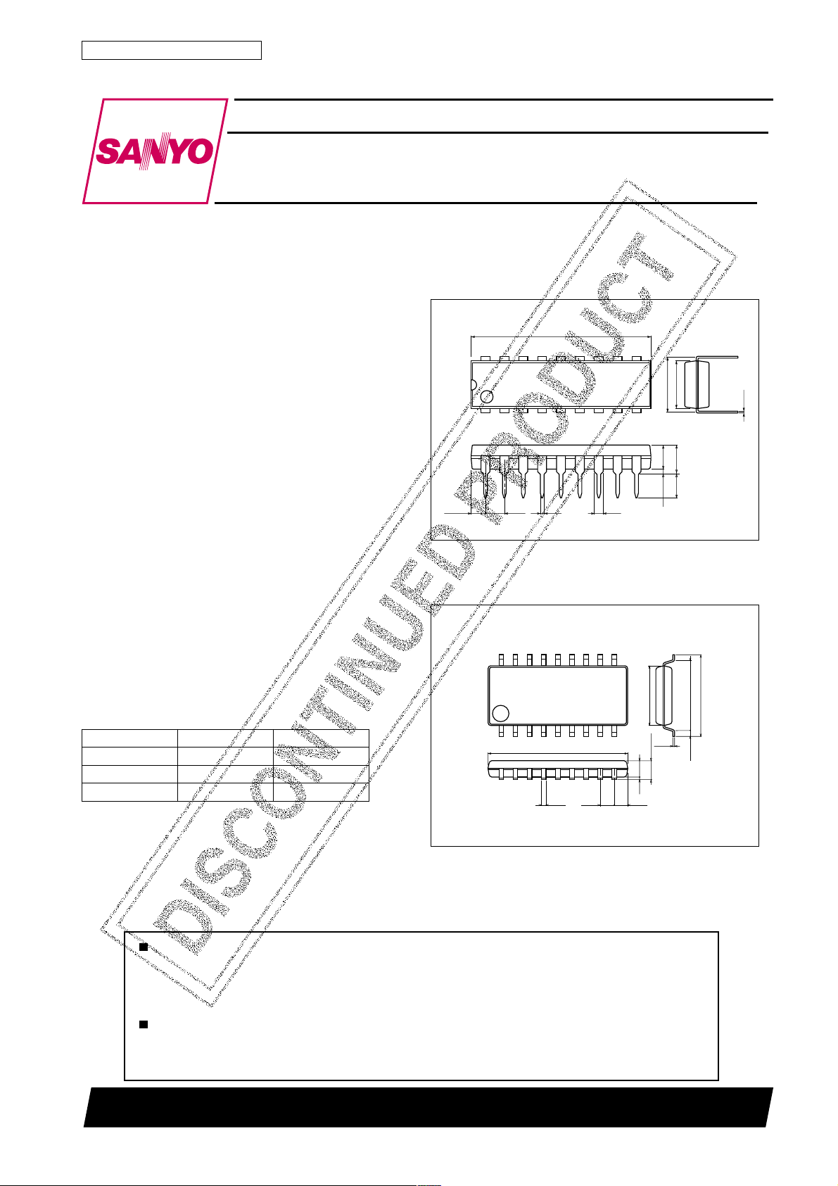
• 18-pin plastic DIP or MFP.
• Optional pull-ups on serial data outputs.
.oNepyTegakcaPpu-lluPtuptuO
N0707CL81PIDoN
MN0707CL81PFMoN
MN1707CL81PFM*seY
*: Only 3 pins for serial data output
Package Dimensions
unit:mm
3007B-DIP18
[LC7070N]
24.0
18
1
(1.84)
2.54
unit:mm
3095-MFP18
[LC7070NM, LC7071NM]
18
1
12.6
0.35
1.27
10
6.4
7.62
0.25
9
(3.25)
3.85max
3.3
1.20.5
10
9
0.51min
SANYO : DIP18
5.4
0.15
1.8max
1.5
0.1
1.22
SANYO : MFP18
6.35
0.625
7.6
71901TN (KT)/O188TA, TS No.2890–1/8
Page 2

Pin Assignment
LC7070N, 7070NM, 7071NM
Top view
Specifications
Absolute Maximum Ratings at Ta = 25˚C, VSS = 0V
retemaraPlobmySsnoitidnoCsgnitaRtinU
egatlovylppusmumixaMV
egatlovtuptuOV
egatlovtupnI
egatlovtuptuOV
tnerructuptuokaePI
egatlovtuptuoegarevA
)lavretnism001(
noitapissidrewopelbawollAdPxam
erutarepmetgnitarepOrpoT 58+ot04–
erutarepmetegarotSgtsT 521+ot55–
Allowable Operating Conditions at T a = –40 to +85˚C, V
retemaraPlobmySsnoitidnoC
egatlovylppusgnitarepOV
egatlovlevel-hgihtupnI
egatlovlevel-woltupnI
noitallicso
rotanosercimarecrofstnatsnocdeetnarauG
DD
V
V
V
I
I
V
V
V
V
V
xamV
1O
1I
2I
3I
2O
PO
AO
AO
DD
1HI
2HI
1LI
2LI
3LI
DD
2CSOVot3.0–
SER,TSETVot3.0–
).2
58+ot04–=aT ° egakcapPID:C082Wm
58+ot04–=aT ° ).3etoNeeS(egakcapPFM:C002Wm
V
DD
SERV8.0
TSETV
SERV
0.7+ot3.0– V
3.0+V
).1etoNeeS(1CSOVot3.0–
).2etoNeeS(1epytNI 51+ot3.0– V
).2etoNeeS(2,1epytTUO 51+ot3.0– V
).2etoNeeS(2,1epytTUO:niphcaeroftnerruckaeP 02+ot2– Am
etoNeeS(2,1epytTUO:niphcaeroftnerrucegarevA
).2etoNeeS(2,1epytTUO:snipllaroftnerruclatoT 09+ot41– Am
= 0V, VDD = 4.5 to 6.0V, unless otherwise specified.
SS
nimpytxam
5.40.6V
).2etoNeeS(1epytNIV7.0
).2etoNeeS(1epytNIV
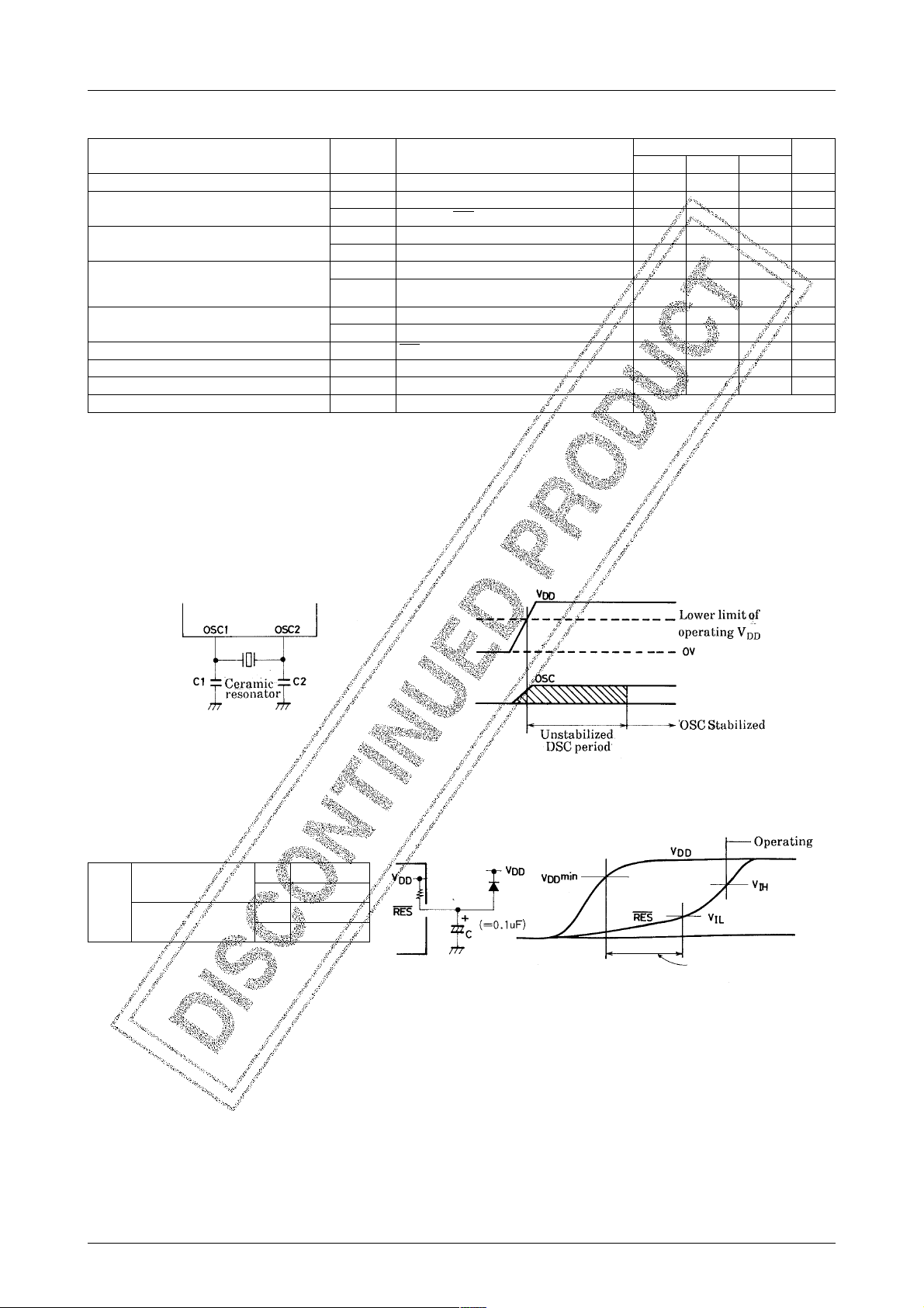
2CSO,1CSO:1erugiFeeS.1elbateeS
DD
DD
SS
SS
SS
DD
3.0+V
DD
3.0+V
DD
02+ot2– Am
˚C
˚C
sgnitaR
V
V3.0
V3.0
V52.0
tinU
5.31V
V
DD
V
DD
V
DD
V
DD
No.2890–2/8
Page 3
LC7070N, 7070NM, 7071NM
Electrical Characteristics at T a = –40 to +85˚C, V
retemaraPlobmySsnoitidnoC
tnerruclevel-hgihtupnII
tnerruclevel-woltupnI
egatlovlevel-hgihtuptuO
)ylnoMN1707CL(
egatlovlevel-woltuptuO
tnerrucegakaelFFOtuptuO
).ylno1epytTUOsiMN1707CL(
egatlovsiseretsyHV
).5etoNeeS(niardtnerruCI
emitnoitazilibatsnoitallicsorotanosercimareCt
emitteseRt
1HI
I
1LI
I
2LI
V
1HO
V
2HO
V
1LO
V
2LO
I
1FFO
I
2FFO
SIH
DD
SFC
TSR
= 0V, VDD = 4.5 to 6.0V, unless otherwise specified.
SS
sgnitaR
nimpytxam
V
NI
VNIV=SS:).2etoNeeS(1epytNI – 0.1Aµ
VNIV=SS:SER – 54 – 01Aµ
IHO=– ).2etoNeeS(2epytTUO:Aµ05
IHO=– ).2etoNeeS(2epytTUO:Aµ01
I
LO
I
LO
).2etoN
V
O
VOV=SS:).2etoNeeS(2,1epytTUO – 0.1Aµ
SERV1.0
).2etoNeeS(1epytNI:V5.31= 0.5Aµ
VDD– 2.1
VDD– 5.0
).2etoNeeS(2,1epytTUO:Am01= 5.1V
eeS(2,1epytTUO:).4etoNeeS(Am8.1=
).2etoNeeS(2,1epytTUO:V5.31= 0.5Aµ
V:1erugiFninwohstiucricgnisU
DD
2CSO,1CSO:2erugiFeeS 01sm
DD
0.401Am
3erugiFeeS
4.0V
tinU
V
V
V
(Note 1) Should be sufficient for oscillation amplitude when oscillator circuit shown in Figure 1 is operated at recom-
mended constants.
(Note 2) OUT type 1 : ERROR, CORRECTION, RECEIVE
OUT type 2 : CLOCK OUT, DATA OUT, DATA START
IN type 1 : CLOCK IN, DATA IN, CORR.SEL, CL.ED.SEL, D.S.CONTROL
(Note 3) Do not use solder dip (dipping in solder tank) when mounting MFP packaged devices to circuit board.
(Note 4) Except for four selectable output pins, other outputs are I
(Note 5) Current drain with N-channel output transistors OFF, and input and output pin voltages = V
at less than 1mA.
OL
DD
.
Figure 1. Oscillator Circuit Figure 2. Stabilization Time
Table 1. Guaranteed Constants
C
1
)ataruM(GM00.4ASC
C
zHM4
2
C
1
)arecoyK(M0.4RBK
C
2
%01±Fp03
%01±Fp03
%01±Fp33
%01±Fp33
Figure 3. Reset Circuit
10ms or more is
recommended allowing
for OSC stabilizing time.
No.2890–3/8
Page 4

LC7070N, 7070NM, 7071NM
Pin Descriptions
langiS
1CSO
2CSO
NIKCOLC5tupnI • .tupnikcolcnoitaludomed)1322AL(SDR tuptuolevel-H
NIATAD6tupnI • .tupniatadnoitaludomed)1322AL(SDR tuptuolevel-H
LES.RROC7tupnI
LES.DE.LC8tupnI
LORTNOC.S.D11tupnI
EVIECER01tuptuO
NOITCERROC21tuptuO
RORRE31tuptuO
TRATSATAD41tuptuO
TUOATAD51tuptuO
TUOKCOLC61tuptuO
SER4tupnI
niP
.oN
1
81
/tupnI
tuptuO
tupnI
• .noitcennocrotanosercimareczHM4
tuptuO
• .tcelesFFO/NOnoitcerrocrorrE
• .atadnoitaludomedSDRrofnoitcerrocrorrestibihni/steS
• .tcelesytiralopkcolcatadlaireS
• .lortnoclangisTRATSATADkcolB
• .langisatadSDRgniviecernehwtuptuO
• .noitcetedcnysretfatuptuoatadlairesgnirudlevel-WOL
• .niardnepO
• .elbanenoitcerrocrorrE
• .elbatcerrocnurodetcerrocsirorreatadlairesfilevel-WOL
• .niardnepO
• .elbanenoitcerrocrorrE
• .elbatcerrocnuerayehtdnasrorreeraerehtfilevel-WOL
• .niardnepO
• .tuptuoatadlairesroflangisTRATSATADkcolB
• atadlaireS
• kcolcatadlaireS
• tesermetsyS
• .selcyckcolc4nahteromroflevel-WOL
noitcerrocoN:0=tupnI
.semitrehtotalevel-HGIH
MN1707CL:pu-lluP
MN1707CL:pu-lluP
MN1707CL:pu-lluP
noitcnuFteseRnoetatS
demrofrepnoitcerroC:1=tupnI
.)egdegnillaftaetadpuatad(
.)egdegnisirtaetadpuatad(
.tupniSERfoemittateS:etoN
.tuptuolangisTRATSATADkcolbllA:0=tupnI
.tuptuolangisTRATSATADkcolb2#ylnO:1=tupnI
.deriuqererasnoitcerroconfilevel-HGIH
MN0707CL,N0707CL:niardnepO
MN0707CL,N0707CL:niardnepO
MN0707CL,N0707CL:niardnepO
tuptuolevel-H
kcolctuptuofoegdegnisirtadelbanetuptuoatadlaireS:0=tupnI
kcolctuptuofoegdegnillaftadelbanetuptuoatadlaireS:1=tupnI
.detelpmocsinoitcerrocrosrorreoneraerehtfilevel-HGIH
tuptuolevel-H
tuptuolevel-H
tuptuolevel-H
tuptuolevel-H
tuptuolevel-H
tuptuolevel-H
tuptuolevel-H
tuptuolevel-H
tuptuolevel-H
System Configuration
No.2890–4/8
Page 5

Timing Charts & Data Format
Serial Data Output
LC7070N, 7070NM, 7071NM
24-bit
data
10ms
Note: All blocks or second block-only output selectable usign D. S. CONTROL input.
No.2890–5/8
Page 6

Serial Data Output Format
LC7070N, 7070NM, 7071NM
EF
srorreoN00
detcerroC01
elbatcerrocnU11
CORR.SEL, D.S.CONTROL Pin Read Timing
• After sync detection
• States CORR. SEL and D. S. CONTROL are read at the start of each RDS demodulation data block. Four consecu-
tive input states are then confirmed, inputs following the fourth are affected.
• During sync detection.
• RED demodulation data bits from LA2231 are read. Four consecutive pin states are confirmed. If all four states are
the same, data are input internally.
No.2890–6/8
Page 7

Serial Data Output Timing (1)
LC7070N, 7070NM, 7071NM
• Serial data outputs from LC7070N, LC7070NM and LC7071NM are delayed one block from the RDS demodulation
data from the LA2231.
• When sync is detected, serial data output starts from the beginning of the next group (1 clock cycle).
• ERROR and CORRECTION signal outputs are generated ahead of the serial data output. These outputs are continu-
ous when errors are detected continuously.
No.2890–7/8
Page 8

Serial Data Output Timing (2)
LC7070N, 7070NM, 7071NM
Specifications of any and all SANYO products described or contained herein stipulate the performance,
characteristics, and functions of the described products in the independent state, and are not guarantees
of the performance, characteristics, and functions of the described products as mounted in the customer's
products or equipment. To verify symptoms and states that cannot be evaluated in an independent device,
the customer should always evaluate and test devices mounted in the customer's products or equipment.
SANYO Electric Co., Ltd. strives to supply high-quality high-reliability products. However, any and all
semiconductor products fail with some probability. It is possible that these probabilistic failures could
give rise to accidents or events that could endanger human lives, that could give rise to smoke or fire,
or that could cause damage to other property. When designing equipment, adopt safety measures so
that these kinds of accidents or events cannot occur. Such measures include but are not limited to protective
circuits and error prevention circuits for safe design, redundant design, and structural design.
In the event that any or all SANYO products(including technical data,services) described or
contained herein are controlled under any of applicable local export control laws and regulations,
such products must not be exported without obtaining the export license from the authorities
concerned in accordance with the above law.
No part of this publication may be reproduced or transmitted in any form or by any means, electronic or
mechanical, including photocopying and recording, or any information storage or retrieval system,
or otherwise, without the prior written permission of SANYO Electric Co. , Ltd.
Any and all information described or contained herein are subject to change without notice due to
product/technology improvement, etc. When designing equipment, refer to the "Delivery Specification"
for the SANYO product that you intend to use.
Information (including circuit diagrams and circuit parameters) herein is for example only ; it is not
guaranteed for volume production. SANYO believes information herein is accurate and reliable, but
no guarantees are made or implied regarding its use or any infringements of intellectual property rights
or other rights of third parties.
This catalog provides information as of July, 2001. Specifications and information herein are subject to
change without notice.
PS No.2890–8/8
 Loading...