

Page 1
Any and all SANYO products described or contained herein do not have specifications that can handle
applications that require extremely high levels of reliability, such as life-support systems, aircraft’s
control systems, or other applications whose failure can be reasonably expected to result in serious
physical and/or material damage. Consult with your SANYO representative nearest you before using
any SANYO products described or contained herein in such applications.
SANYO assumes no responsibility for equipment failures that result from using products at values that
exceed, even momentarily, rated values (such as maximum ratings, operating condition ranges,or other
parameters) listed in products specifications of any and all SANYO products described or contained
herein.
CMOS IC
4-bit Microcontroller with Built-in PROM
Ordering number:ENN3492
LC66P408
SANYO Electric Co.,Ltd. Semiconductor Company
TOKYO OFFICE Tokyo Bldg., 1-10, 1 Chome, Ueno, Taito-ku, TOKYO, 110-8534 JAPAN
Overview
The LC66P408 is a 4-bit microcontroller with a built-in 8
Kbyte PROM. It is compatible with the LC6640X series
mask ROM devices, making it ideal for prototyping and
software development and testing.
The LC66P408 features 33 user-defined options comprising output configuration, output level after reset, watchdog timer and oscillator configuration options. The output
configuration options are open-drain, open-drain with pullup, and CMOS. The oscillator options are ceramic resonator, RC oscillator and external clock.
The LC66P408 operates from a 5 V supply and is a v ailable
in 42-pin DIPs and 48-pin QFPs.
Features
• 33 user-defined options including port output configuration, output level after reset and watchdog timer options
• Ceramic resonator, RC oscillator or external cloc k option
• 8 Kbyte PRQM (0000H to 2007H user addressable)
• Compatible with the LC6640X series mask ROM devices
• 0.92 to 10.0 µs instruction cycle time
• 5 V supply
• 42-pin DIP and 48-pin QFP
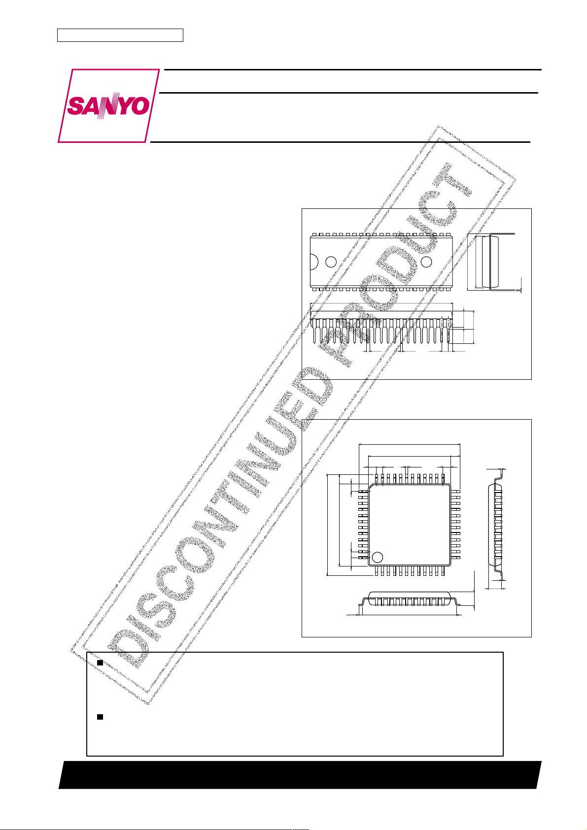
Package Dimensions
Unit:mm
3025B-DIP42S
[LC66P408]
42
1
Unit:mm
3156-QIP48E
1.6
1.5
37.9
0.95
1.5
36
37
0.48
[LC66P408]
17.2
14.0
0.35
1.0
1.78
22
21
1.15
SANYO : DIP42S
1.6
1.5
25
15.24
4.25
5.1max
3.8
0.51min
24
13.8
0.25
0.15
14.0
17.2
1.0
48
1.5
1
0.8
15.6
O2501TN (KT)/4092JN No.3492–1/14
13
12
3.0max
SANYO : QIP48E
0.1
2.7
Page 2
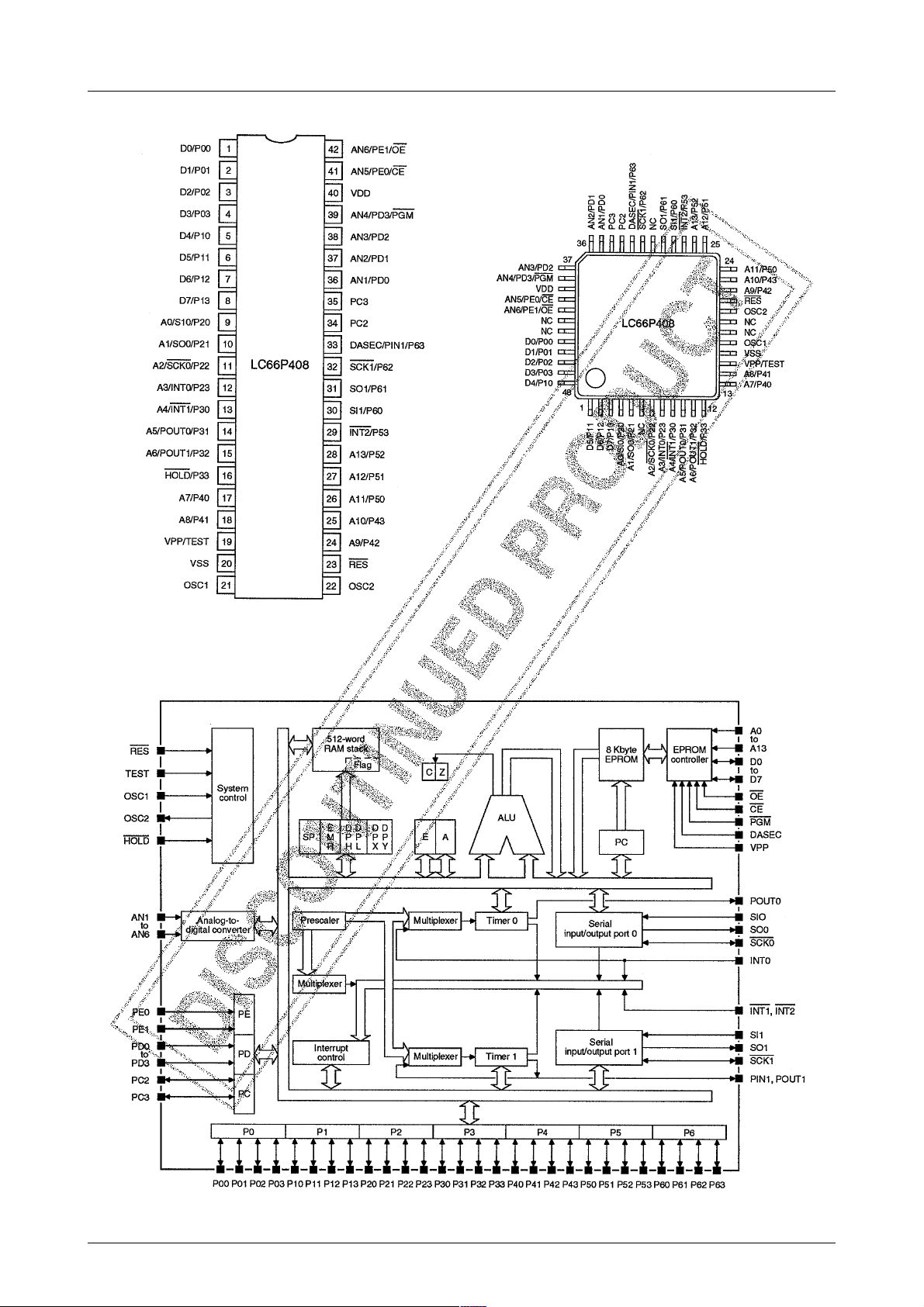
Pin Assignments
LC66P408
Block Diagram
Top view
No.3492–2/14
Page 3

Pin Function
rebmuN
S24PIDE84PIQ
14400P/0D
25410P/1D
36420P/2D
47430P/3D
58401P/4D
61 11P/5D
72 21P/6D
83 31P/7D
94 02P/0IS/0A
015 12P/0OS/1A
117 22P/0KCS/2A
218 32P/0TNI/3A
319 03P/1TNI/4A
410113P/0TUOP/5A
511123P/1TUOP/6A
612133P/DLOH )DLOH(tupnilortnocedom-dlohdna)33P(troptupnitib-elgnisdexelpitluM
713104P/7A
814114P/8A
422224P/9A
523234P/01A
9151TSET/PPVtupnitsetUPC
0261VSSdnuorG
12711CSO
22022CSO
3212SERtupniteseR
624205P/11A
725215P/21A
826225P/31A
927235P/2TNI
038206P/1IS
139216P/1OS
231326P/1KCS
332336P/1NIP/CESAD
43332CP
53433CP
63530DP/1NA
73631DP/2NA
83732DP/3NA
9383MGP/3DP/4NA
0493VDDylppusV5
1404EC/0EP/5NA
2414EO/1EP/6NA
–
34,24
LC66P408
emaNnoitpircseD
)3Dot0D(senil
)7Dot4D(senil
)3Aot0A(senilsubsserdda
)01Aot7A(senil
snoitcennocrotallicsolanretxE
)31Aot11A(senilsubsserddaMORPdna
)CESAD(tupnilortnocytirucesatad
CPtroptuptuo/tupnitib-2
)4NAot1NA(stupniretrevnoclatigid-ot-golanadna)MGP(
,03,91,81,6
CNnoitcennocoN
subatadMORPdna)30Pot00P(0Ptroptuptuo/tupnitib-4dexelpitluM
subatadMORPdna)31Pot01P(1Ptroptuptuo/tupnitib-4dexelpitluM
laires,)0IS(0tupnilaires,)32Pot02P(2Ptroptuptuo/tupnitib-4dexelpitluM
MORPdna)0TNI(0tseuqertpurretnI,)0KCS(0kcolclaires,)0OS(0tuptuo
,)1TNI(1tseuqertpurretni,)23Pot03P(3Ptroptuptuo/tupnitib-3dexelpitluM
)6Aot4A(senilsubsserddaMORPdna)1TUOPdna0TUOP(stuptuoremit
subsserddaMORPdna)34Pot04P(4Ptroptuptuo/tupnitib-4dexelpitluM
)2TNI(2tseuqertpurretni,)35Pot05P(5Ptroptuptuo/tupnitib-4dexelpitluM
laires,)1IS(1tupnilaires,)36Pot06P(6Ptroptuptuo/tupnitib-4dexelpitluM
MORPdna)1NIP(tupniretnuoctneve,)1KCS(1kcolclaires,)1OS(1tuptuo
tupnilortnocmargorpMORP,)3DPot0DP(DPtroptupnitib-4dexelpitluM
dna)EC(elbanepihcMORP,)1EPot0EP(EPtroptupnitib-2dexelpitluM
)6NAdna5NA(stupniretrevnoclatigid-ot-golanadna,)EO(elbanetuptuo
No.3492–3/14
Page 4

LC66P408
Specifications
Absolute Maximum Ratings
retemaraPlobmySsnoitidnoCsgnitaRtinU
egatlovylppuSV
egatlovtupni)33Pgnidulcxe(6Pot2PstroPV
stupnillarofegnaregatlovtupnIV
egatlovtuptuo)33Pgnidulcxe(6Pot2PstroPV
stuptuollarofegnaregatlovtuptuOV
tnerrucecruostuptuo5Pdna,4P,1P,0PstroPI–
CPdna6P,)33Pgnidulcxe(3P,2PstroP
tnerrucecruostuptuo
tuptuoCPdna)33Pgnidulcxe(6Pot0PstroP
tnerrucknis
14Pdna04P,)33Pgnidulcxe(3Pot0PstroP
tnerrucknislatot
knislatotCPdna6P,5P,34P,24PstroP
tnerruc
14Pdna04P,)33Pgnidulcxe(3Pot0PstroP
tnerrucecruoslatot
ecruoslatotCPdna6P,5P,34P,24PstroP
tnerruc
noitapissidrewopelbawollAP
noitapissidrewopelbawollAP
erutarepmetgnitarepOrpoT 07+ot03–
erutarepmetegarotSgtsT 521+ot55–
DD
1I
2I
1O
2O
1PO
I–
2PO
I
NO
I
1NO
I
2NO
I–
1PO
I–
2PO
1D
2D
1etoneeS 0.51+ot3.0– V
2etoneeSVot3.0–
1etoneeS 0.51+ot3.0– V
2etoneeSVot3.0–
S24PID 006Wm
3etoneeS,E84PIQ 034Wm
Notes
1. Open-drain output configuration option
2. All output configuration options
3. Heat-soak the QIP package before mounting. Do not immerse the package in the solder dip tank when mounting the
QIP on the substrate, and avoid prolonged contact with the solder.
0.7+ot3.0– V
3.0+V
DD
3.0+V
DD
2Am
4Am
02Am
57Am
57Am
52Am
52Am
˚C
˚C
Recommended Operating Conditions at Ta = 25°C, V
retemaraPlobmySsnoitidnoCsgnitaRtinU
egatlovylppuSV
egnaregatlovylppuSV
noitneter
atadrofegnaregatlovylppusedom-dloH
DD
DD
V
DD
SS
= 0V
Electrical Characteristics at T a = –30 to +70°C, VDD = 4.5 to 5.5V, VSS = 0V unless otherwise noted
retemaraPlobmySsnoitidnoC
rotanosercimareczHM45.40.8Am
tnerrucylppusedom-teseRI
tnerrucylppusedom-tlaHI
tnerrucylppusedom-dloHI
SER.6Pdna5P,)33Pgnidulcxe(3P,2PstroP
egatlovlevel-woltupni1CSOdna
egatlovlevel-woltupni33P/DLOHV
TSETdnaEPdnaDP,CP,4P,1P,0PstroP
egatlovlevel-woltupni
level-hgihtupni)33Pgnidulcxe(6Pot2PstroP
egatlov
level-hgihtupni1CSOdnaSER,33P/DLOH
egatlov
level-hgihtupniEPdnaDP,CP,1P,0PstroP
egatlov
tuptuoCPdna)33Pgnidulcxe(6Pot0PstroP
egatlovlevel-wol
CPdna6P,)33Pgnidulcxe(3P,2PstroP
egatlovlevel-hgihtuptuo
level-hgihtuptuo5Pdna4P,1P,0PstroP
egatlov
DD
THDD
V
DHDD
DD
V
1LI
V
2LI
V
3LI
V
V
V
V
LO
V
V
DD
1HI
2HI
3HI
I
LO
I
LO
I
HO
1HO
I
HO
V
DD
2HO
I
HO
kcolclanretxezHM45.60.11Am
rotallicsoCR48Am
rotanosercimareczHM40.35.5Am
kcolclanretxezHM45.30.6Am
rotallicsoCR0.35.5Am
V5.5ot8.1=10.00.01Aµ
.1etoneeS
V5.5ot8.1=V
.1etoneeS
.2etoneeS
.1etoneeS
Am6.1= 4.0
Am6.1= 5.1
I,V5.4=
HO
.FFOrotsisnartlennahc-ntuptuO
.FFOrotsisnartlennahc-ntuptuO
.FFOrotsisnartlennahc-ntuptuO
FFOrotsisnartlennahc-ntuptuO
.FFOrotsisnartlennahc-ntuptuO
.3etoneeS.Am1–=V
.3etoneeS.Am1.0–=V
.4etoneeS.Am2.0–=4.2
.4etoneeS.Am31.0–=
nimpytxam
V
SS
SS
V
SS
V57.0
DD
V57.0
DD
V7.0
DD
0.1–
DD
5.0–
DD
V
53.1–
DD
sgnitaR
Continued on next page.
5V
5.5ot5.4V
5.5ot8.1V
tinU
V52.0
V
DD
V52.0
V
DD
V3.0
V
DD
5.31V
V
V
DD
V
V
DD
V
V
V
No.3492–4/14
Page 5

LC66P408
Continued from preceding page.
retemaraPlobmySsnoitidnoC
1CSOdnaSERdna,6Pdna5P,3P,2PstroP
V
egatlovdlohserhtlevel-wolreggirt-ttimhcS
1CSOdnaSERdna,6Pdna,5P,3P,2PstroP
egatlovdlohserhtlevel-hgihreggirt-ttimhcS
1CSOdnaSER,6Pdna5P,3P,2PstroP
egatlovsiseretsyhreggirt-ttimhcS
stupnillaroftnerruclevel-woltupnII
tnerruc
tnerruclevel-hgihtupni
tnerruc
noitpopu-llup
ycneuqerftupnirotanosercimareCf
ycneuqerftupnirotallicsoCRf
ecnaticapacrotallicsoCRlanretxEC
ecnatsiserrotallicsoCRlanretxER
level-hgihtupni)33Pgnidulcxe(6Pot2PstroP
1CSOdnaSERdna,33Pdna1P,0PstroP
level-hgihtupniEPdnaDP,3CP,2CPstroP
tnerrucegakaeltuptuo6Pot2PstroPI
tnerrucegakaeltuptuoCPdna1P,0PstroPI
htiwtnerructuptuo5Pdna4P,1P,0PstroP
emitnoitazilibatstupnirotanosercimareCf
Notes
1. Ports with CMOS output configuration option cannot be used as input ports.
2. Open-drain output configuration option
3. CMOS output configuration option
4. Pull-up output configuration option
Lt
V
Ht
V
SYH
VIV=
V
I
VIV=
VIV=
V
I
VIV=
VIV=
SS
.2etoneeS
.2etoneeS
DD
.1etoneeS
DD
.1etoneeS
DD
SSV,DD
Ω
k2.2=R
.2etoneeS.V5.31=
.2etoneeS.
%1±Fp001=C,%1±23
LI
I
1HI
I
2HI
I
3HI
1FFO
2FFO
I
OP
FC
SFC
CR
txe
txe
sgnitaR
nimpytxam
V52.0
DD
V5.0
DD
V1.0
.FFOrotsisnartlennahc-ntuptuo,
.FFOrotsisnartlennahc-ntuptuo,V5.31=
.FFOrotsisnartlennahc-ntuptuo,
.FFOrotsisnartlennahc-ntuptuo,
.4etoneeS.V5.5=6.1– Am
1– Aµ
V5.0
DD
V57.0
DD
DD
5
1
1
5
1
4zHM
01
4
001Fp
2.2k
tinU
V
V
V
Aµ
Aµ
Aµ
Aµ
Aµ
sm
zHM
Ω
A/D converter characteristics at Ta = –30 to +70 °C, V
retemaraPlobmySsnoitidnoC
noituloseRseR 6tib
ycaruccaetulosbAA
rorreytiraeniLniL 5.0±1±bsI
egatlovtupnigolana6NAot1NAV
emitnoisrevnocdeeps-woLt
emitnoisrevnocdeeps-hgiHt
SBA
DANI
LDAC
HDAC
= 4.5 to 5.5 V, VSS = 0V
DD
Comparator characteristics at Ta = –30 to +70 °C, VDD = 4.5 to 5.5 V, VSS = 0V
retemaraPlobmySsnoitidnoC
ycaruccarotarapmoc6NAot1NAA
egatlovdlohserht6NAot1NAV
egatlovtupnigolana6NAot1NAV
egatlovtupni6NAot1NAV
emitnoisrevnoCt
MCEC
MCHT
DANI
MCNI
MCC
sgnitaR
nimpytxam
1±5.1±bsI
V
SS
t821
CYC
t46
CYC
sgnitaR
nimpytxam
1±5.1±bsI
5.0±1±bsI
V
SS
V
SS
V
t652
t821
V
V
DD
CYC
CYC
DD
DD
03sµ
tinU
V
sµ
sµ
tinU
V
V
No.3492–5/14
Page 6

Timing Characteristics
Serial input/output timing
LC66P408
Ta = –30 to +70 °C, V
emitelcycnoitcurtsnIt
= 4.5 to 5.5 V, VSS = 0 V
DD
retemaraPlobmySsnoitidnoC
emitelcyctupnikcolclaires1KCSdna0KCSt
emitelcyctuptuokcolclaires1KCSdna0KCSt
htdiwesluptupnikcolclaires1KCSdna0KCSt
htdiwesluptuptuokcolclaires1KCSdna0KCSt
emitesirtuptuokcolclaires1KCSdna0KCSt
emitllaftuptuokcolclaires1KCSdna0KCSt
emitputesatadlaires1ISdna0ISt
emitdlohatadlaires1ISdna0ISt
yaledtuptuoatadlaires1OSdna0OSt
CYC
YCKC
YCO
LKC
HKC
RKC
FKC
KCI
IKC
OKC
Note
Each test input and output has an RC load as shown in the following figure.
External clock timing
sgnitaR
nimpytxam
29.001sµ
9.0sµ
t2
CYC
4.0sµ
t
CYC
3.0sµ
3.0sµ
tinU
sµ
sµ
1.0sµ
1.0sµ
3.0sµ
Ta = –30 to +70 °C, VDD = 4.5 to 5.5 V, VSS = 0 V
retemaraPlobmySsnoitidnoC
ycneuqerftupnikcolclanretxe1CSOf
htdiwesluplevel-woltupnikcolclanretxe1CSOt
htdiwesluplevel-hgihtupnikcolclanretxe1CSOt
emitesirtupnikcolclanretxe1CSOt
emitllaftupnikcolclanretxe1CSOt
txe
Ltxe
Htxe
Rtxe
Ftxe
sgnitaR
nimpytxam
4.053.4zHM
07sn
07sn
No.3492–6/14
tinU
03sn
03sn
Page 7

Interrupt and reset timing
LC66P408
Ta = –30 to +70 °C, V
= 4.5 to 5.5 V, VSS = 0 V
DD
retemaraPlobmySsnoitidnoC
htdiwesluplevel-wol0TNIt
htdiwesluplevel-hgih0TNIt
htdiwesluplevel-wol2TNIdna1TNIt
htdiwesluplevel-hgih2TNIdna1TNIt
htdiwesluplevel-woltupni1NIPt
htdiwesluplevel-hgihtupni1NIPt
htdiwesluplevel-woltupniSERt
htdiwesluplevel-hgihtupniSERt
LOI
HOI
L1I
H1I
LNIP
HNIP
LSR
HSR
sgnitaR
nimpytxam
t2
CYC
t2
CYC
t2
CYC
t2
CYC
t2
CYC
t2
CYC
t3
CYC
t3
CYC
tinU
sµ
sµ
sµ
sµ
sµ
sµ
sµ
sµ
Input and Output Functions
The LC66P408 has many multiplexed pins whose function is controlled by software. The function of each of these pins
is shown in the following table.
emaN noitcnuF
00P/0D
10P/1D
20P/2D
30P/3D
01P/4D
11P/5D
21P/6D
31P/7D
02P/0IS/0A
12P/0OS/1A
22P/0KCS/2A
32P/0TNI/3A
03P/1TNI/4A
13P/0TUOP/5A
23P/1TUOP/6A
33P/DLOH
04P/7A
14P/8A
24P/9A
34P/01A
05P/11A
15P/21A
25P/31A
35P/2TNI
06P/1IS
16P/1OS
26P/1KCS
36P/1NIP/CESAD
2CP
3CP
0DP/1NA
1DP/2NA
2DP/3NA
MGP/3DP/4NA
.desserdda
.edomdlohgnirudderongiera
.snoitcnuflortnocedom-tlahevahoslayehT.desserdda
.0remitgnisutupniretnuoctnevednatnemerusaemhtdiweslup,tseuqertpurretninasa32P
.tuptuoMWPadna1remitmorftuptuoevaw-erauqsasa23Pdna0remit
.desserddasiyromemnehwstupnisubsserdda
.tupnitseuqertpurretninasanoitcnufosla35PtroP.desserddasiyromemnehwstupnisubsserddasanoitcnuf
.stroptib-elgnis,owtrotroptib-2arehtiesadesserddaebnac3CPdna2CPstroP
.tupnilortnocmargorpyromemehtsasnoitcnufosla3DPtrop,noitiddanI.stupni
Continued on next page.
No.3492–7/14
siyromemnehwsenilsubatadsanoitcnufyehT.stroptib-elgnisruofrotroptib-4arehtiesadesserddaebnac3OPot00PstroP
siyromemnehwsenilsubatadsanoitcnufyehT.stroptib-elgnis,ruofrotroptib-4arehtiesadesserddaebnac31Pot01PstroP
nehwstupnisubsserddasanoitcnufyehT.stroptib-elgnisruofrotroptib-4arehtiesadesserddaebnac32Pot02PstroP
dnakcolcatadlairesasa22P,tuptuoatadlairesasa12P,tupniatadlairesasasnoitcnufosla02PtroP.desserddasiyromem
sserddasanoitcnufyehT.stroptib-elgnis,eerhtro33Phtiwtroptib-4a,troptib-3arehtiesadesserddaebnac23Pot03PstroP
morftuptuoevaw-erauqsasa13P,tupnitseuqertpurretninasasnoitcnufosla03PtroP.desserddasiyromemnehwstupnisub
tupnilortnocedom-dlohehtsanoitcnuffI.troptib-elgnisaro23Pot03Phtiwtroptib-4arehtiesadesserddaebnac33PtroP
SERnoslangisteseR.niagaHGIHseog33PnehwstratserUPCehT.detucexesinoitcurtsniDLOHehtdnaWOLsi33Pnehw
sanoitcnufyehT.35Pot05Phtiwtroptib-8narostroptib-elgnisruof,troptib-4arehtiesadesserddaebnac34Pot04PstroP
25Pot05PstroP.34Pot04Phtiwtroptib-8narostroptib-elgnisruof,troptib-4arehtiesadesserddaebnac35Pot05PstroP
16P,tupniatadlairesasanoitcnufosla06PtroP.stroptib-elgnisruofrotroptib-4arehtiesadesserddaebnac36Pot06PstroP
.tupniretnuoctneve1remitdnatupnilortnocytirucesatadasa36Pdnakcolcatadlairesasa26P,tuptuoatadlairesasa
retrevnoclatigid-ot-golanasanoitcnufoslayehT.stroptib-elgnisruofrotroptib-4arehtiesadesserddaebnac3DPot0DPstroP
Page 8

LC66P408
Continued from preceding page.
emaN noitcnuF
EC/0EP/5NA
EO/1EP/6NA
1CSO
2CSO
SER .tesersiUPCeht,HGIHsi33P/DLOHetihwWOLseogSERnehW
TSET/PPVdnuorgotdetcennocyllamroN.tupnitsetUPC
User Options
Oscillator Options
There are three user options for the oscillator : an external clock, an RC oscillator and a ceramic resonator. The
internal circuits of OSC1 and OSC2 for the external clock,
RC oscillator and ceramic resonator options are shown in
figures 1, 2 and 3, respectively. Note the Schmitt-trigger
inputs for both the external clock and RC oscillator options.
Figure 1. External clock option
.nepotfel
.stupniretrevnoclatigid-ot-golanasanoitcnufoslayehT.desserddasiyromemnehw,ylevitcepser
,elbaneetirwdnaelbanepihcsanoitcnufyehT.stroptib-elgnisowtrotroptib-2arehtiesadesserddaebnac1EPot0EPstroP
si2CSO,desusikcolclanretxenanehW.snoitcennocrotallicsoCRrorotanosercimareclanretxeehtsanoitcnuf2CSOdna1CS
Figure 4. N-channel open-drain option
The p-channel pull-up option for ports P0, P1, P4 and P5
results in an n-channel sink transistor with a p-channel,
active pull-up transistor configuration, and for ports P2,
P3, P6 and PC, a CMOS configuration.
Figure 2. RC oscillator option
Figure 3. Ceramic resonator option
Output Options
There are two user options for the output configuration of
each port-n-channel open drain and p-channel, active pullup, shown in figures 4 and 5, respectively. Ports P2, P3,
P5 and P6 have Schmitt-trigger inputs in both output configurations.
Figure 5. P-channel pull-up option
The n-channel open-drain outputs for ports P2 to P6 have
a withstand voltage greater than 15 V.
Output Level After Reset Option
The output level of ports P0 and P1 after a CPU reset is
user selectable.
Watchdog Timer Option
A watchdog timer is available to prevent program runaway.
No.3492–8/14
Page 9

LC66P408
PROM Specification
Specifying Programs and Options
The user-addressable memory is 0000H to 2007H.
Addresses 0000H to 1FFFH are for user programs, and
addresses 2000H to 2007H, for option specification. The
option specification is coded using the information shown
in the following table.
sserddAtibataDretemaraP
0DnoitcnufremitgodhctaW oNseY
1Dteserretfalevel0PtroP WOLHGIH
H0002
H1002
H2002
H3002
H4002
H50027Dot0DnoitcnufoN 0otteS
H60027Dot0DnoitcnufoN 0otteS
H7002
2Dteserretfalevel1PtroP WOLHGIH
3DnoitcnufoN 0otteS
4DrotallicsO
7Dot5DnoitcnufoN 0otteS
0Dnoitarugifnoctuptuo00PtroP
1Dnoitarugifnoctuptuo10PtroP
2Dnoitarugifnoctuptuo20PtroP
3Dnoitarugifnoctuptuo30PtroP
4Dnoitarugifnoctuptuo01PtroP
5Dnoitarugifnoctuptuo11PtroP
6Dnoitarugifnoctuptuo21PtroP
7Dnoitarugifnoctuptuo31PtroP
0Dnoitarugifnoctuptuo02PtroP
1Dnoitarugifnoctuptuo12PtroP
2Dnoitarugifnoctuptuo22PtroP
3Dnoitarugifnoctuptuo32PtroP
4Dnoitarugifnoctuptuo03PtroP
6Dnoitarugifnoctuptuo23PtroP
7DnoitcnufoN 0otteS
0Dnoitarugifnoctuptuo04PtroP
1Dnoitarugifnoctuptuo14PtroP
2Dnoitarugifnoctuptuo24PtroP
3Dnoitarugifnoctuptuo34PtroP
4Dnoitarugifnoctuptuo05PtroP
5Dnoitarugifnoctuptuo15PtroP
6Dnoitarugifnoctuptuo25PtroP
7Dnoitarugifnoctuptuo35PtroP
0Dnoitarugifnoctuptuo06PtroP
1Dnoitarugifnoctuptuo16PtroP
2Dnoitarugifnoctuptuo26PtroP
3Dnoitarugifnoctuptuo36PtroP
7Dot4DnoitcnufoN 0otteS
1D,0DnoitcnufoN 0otteS
2Dnoitarugifnoctuptuo2CPtroP
3Dnoitarugifnoctuptuo3CPtroP
7Dot4DnoitcnufoN 0otteS
01
kcolc
niard-nepOpu-lluP
niard-nepOpu-lluP
niard-nepOpu-lluP
niard-nepOpu-lluP5Dnoitarugifnoctuptuo13PtroP
niard-nepOpu-lluP
niard-nepOpu-lluP
niard-nepOpu-lluP
niard-nepOpu-lluP
noitpO
lanretxerorotallicsoCR
rotanosercimareC
Note
Ports with CMOS output configuration cannot be used as input ports.
The assembler execute command when specifying programs and options using a SANYO cross assembler is LC66S .EXE.
No.3492–9/14
Page 10

LC66P408
PROM Programming
The PROM can be programmed using a special adapter
board, W66EP308D/408D for the 42-pin DIP and
W66EP308Q/408Q for the 48-pin QIP as shown in the
following figure, and a universal EPROM programmer.
The PROM address range is 0000H to 2007H, Addresses
2008H and above cannot be either programmed or read.
The EPROM programmer should be Intel 27128 compatible with V
= 21 V . The recommended program-
PP
mers are shown in the following table. Please contact your
nearest SANYO representative if you intend to use an
alternative EPROM programmer.
Manufacturer
ADVANTEST
SANYO
TR4943, R4944A, R4945 or equivalent
EVA850 or EVA800 special-purpose
Model
programmers
Note
Intel is a registered trademark of Intel Corporation.
ADVANTEST is a registered trademark of ADVANTEST
Corporation.
The EPROM programmer adapter incorporates a data
security switch. When this switch is ON, data is secure,
and when OFF, the data lines are floating and the PROM
can be programmed. Note that when the data lines are
floating, the EPROM programmer will return an error.
This error can be ignored.
No.3492–10/14
Page 11

LC66P408
APPLICATION NOTES
Reset Timing
The reset signal on RES should be held LOW for a minimum of three instruction cycles after the oscillator has
stabilized to ensure correct operation, as shown in the
following figure.
After a reset occurs, all I/O ports are reset to open-drain
output configuration with floating outputs, except for ports
P0 and P1 which both have an output level after reset
option. The output configuration of each port is then set
using the specified options during the eight instruction
cycles after RES goes HIGH. Program execution then
begins from address 0000H.
The LC66E408/P408 can also be reset while in hold mode
(HOLD/P33 is LOW) as long as hold mode is exited before RES goes HIGH again.
Reference Clock
The external circuit for a ceramic resonator is shown in
figure 6, and the recommended resonator and component
values, in the following table. The oscillator stabilization characteristics are shown in figure 7.
Figure 6. Ceramic resonator
No.3492–11/14
Page 12

LC66P408
rotanosercimareC
GM00.4–ASCataruMzHM4%01±Fp33%01±Fp33
SM0.4–RBKarecoyKzHM4%01±Fp33%01±Fp33
GM00.4–TSCataruMzHM4
roticapaclanretnihtiw
SEM0.4–RBKarecoyKzHM4
roticapaclanretnihtiw
1C2C
A/NA/N
A/NA/N
ecnaticapaC
Figure 7. Ceramic resonator stabilization time
The external circuit for an RC oscillator is shown in the
following figure.
The external clock input connection is OSC1. The remaining oscillator connection, OSC2, should be left open as
shown in the following figure.
The RC oscillator frequency is detemined by the external resistor and capacitor and has only been specified for
Rext = 2.2 kΩ and Cext = 100 pF. The frequency for other
values of Rext and Cext can be determined from the graph
in the following figure.
Preparation Procedure
The preparation procedures shown in the following figure for DIP and QFP packages should always be followed
prior to mounting the packages on the substrate.
Note that the QIP package should be heat-soaked for 24
hours at 125 °C immediately prior to mounting.
No.3492–12/14
Page 13

LC66P408
Screening procedure
The construction of the microcontroller with a blank builtin PROM makes it impossible for SANYO to completely
factory-test it before shipping. To prove reliability of the
programmed devices, the screening procedure shown in
the following figure should always be followed.
Ordering Information
When ordering identical mask ROM and PROM devices
simultaneously, provide an EPROM containing the target
memory contents together with separate order forms for
each of the mask ROM and PROM versions.
When ordering a PROM device, provide an EPROM containing the target memory contents together with an order
from.
When ordering either an LC66404A 4 Kbyte or LC66406A
6 Kbyte mask ROM device, insert a jump command, or
retemaraPlobmySnoitidnoC804P66CLseiresX0466CLtinU
egnaregatlovylppusdednemmoceRV
terrucylppusedom-tlahmumixaMI
ecnaticapacrotallicsoCRlanretxEC
ecnatsiserrotallicsoCRlanretxEtxeR2.27.2kΩ
teserretfanoitarugifnoctuptuotroP
DD
THDD
rotallicsoCR5.55.5
txe
A breakdown of the LC66 series devices, which includes the LC66408 and LC6640X devices, is shown in the following
table.
Note that it is not possible to perform a write test on the
blank PROM. 100% yield, therefore, cannot be guaranteed.
any similar command, to avoid executing an address beyond the range of the target device. In addition, write a 0
into all locations above 2007H.
A comparison of the LC66P408 characteristics with those
of the LC6640X mask ROM devices is shown in the following table.
5.5ot5.40.6ot0.4V
rotanosercimareczHM45.50.3
AmkcolclanretxezHM40.65.3
001001Fp
0P(niard-nepO
osla1Pdna
)pu-llupevah
ybdeificepS
noitporesu
eciveDniPyticapacMORyticapacMARepytegakcaP
A803/A603/A40366CL24MORetybK8/6/4
803E66CL24MORPEetybK8 84CFQroS24CID
803P66CL24MORPetybK8 E84PIQroS24PID
804/A604/A40466CL24MORetybK8/6/4 E84PIQroS24PID
804E66CL24MORPEetybK8 84CFQroS24CID
804P66CL24MORPetybK8 E84PIQroS24PID
B615/B215/B805/B60566CL46MORetybK61/21/8/6 A46PIQroS46PID
615E66CL46MORPEetybK61 46CFQroS46CID
615P66CL46MORPetybK61 E46PIQroS46PID
setyb215
E84PIQroS24PID
SANYO ROM Services
SANYO offers various services at nominal charges. These include ROM writing, ROM reading, and package stamping
and screening. Contact your local SANYO representative for further information.
No.3492–13/14
Page 14

LC66P408
Specifications of any and all SANYO products described or contained herein stipulate the performance,
characteristics, and functions of the described products in the independent state, and are not guarantees
of the performance, characteristics, and functions of the described products as mounted in the customer's
products or equipment. To verify symptoms and states that cannot be evaluated in an independent device,
the customer should always evaluate and test devices mounted in the customer's products or equipment.
SANYO Electric Co., Ltd. strives to supply high-quality high-reliability products. However, any and all
semiconductor products fail with some probability. It is possible that these probabilistic failures could
give rise to accidents or events that could endanger human lives, that could give rise to smoke or fire,
or that could cause damage to other property. When designing equipment, adopt safety measures so
that these kinds of accidents or events cannot occur. Such measures include but are not limited to protective
circuits and error prevention circuits for safe design, redundant design, and structural design.
In the event that any or all SANYO products(including technical data,services) described or
contained herein are controlled under any of applicable local export control laws and regulations,
such products must not be exported without obtaining the export license from the authorities
concerned in accordance with the above law.
No part of this publication may be reproduced or transmitted in any form or by any means, electronic or
mechanical, including photocopying and recording, or any information storage or retrieval system,
or otherwise, without the prior written permission of SANYO Electric Co. , Ltd.
Any and all information described or contained herein are subject to change without notice due to
product/technology improvement, etc. When designing equipment, refer to the "Delivery Specification"
for the SANYO product that you intend to use.
Information (including circuit diagrams and circuit parameters) herein is for example only ; it is not
guaranteed for volume production. SANYO believes information herein is accurate and reliable, but
no guarantees are made or implied regarding its use or any infringements of intellectual property rights
or other rights of third parties.
This catalog provides information as of October, 2001. Specifications and information herein are subject
to change without notice.
PS No.3492–14/14
 Loading...