

Page 1

Any and all SANYO products described or contained herein do not have specifications that can handle
applications that require extremely high levels of reliability, such as life-support systems, aircraft’s
control systems, or other applications whose failure can be reasonably expected to result in serious
physical and/or material damage. Consult with your SANYO representative nearest you before using
any SANYO products described or contained herein in such applications.
SANYO assumes no responsibility for equipment failures that result from using products at values that
exceed, even momentarily, rated values (such as maximum ratings, operating condition ranges,or other
parameters) listed in products specifications of any and all SANYO products described or contained
herein.
CMOS IC
4-bit Single Chip Microcontroller with EPROM
Ordering number:ENN*2928A
LC66E516
SANYO Electric Co.,Ltd. Semiconductor Business Headquarters
TOKYO OFFICE Tokyo Bldg., 1-10, 1 Chome, Ueno, Taito-ku, TOKYO, 110-8534 JAPAN
Preliminary
Overview
The LC66E516 is a 4-bit single-chip microcontroller with
an EPROM on-chip, and can be used for developing and
evaluating application programs for the LC665XX series
4-bit single-chip microcontrollers.
The LC66E516 microcontroller is a 4-bit single-chip IC
with an EPROM on-chip and brought to you in ceramic
DIC64S package with a window and ceramic QFC64 package with a window. This window permits the user to erase
EPROM program data as many times as he or she wants.
Then, it could be said that this single-chip IC is best suited
for developing application programs.
The LC66E516 microcontroller has the same function and
the pin assignment as those of the 4-bit single-chip mask
programmed ROM-version LC66E516 microcontroller . The
on-chip EPROM is 16k bytes in size.
Features
• Optional functions user-selectable by speciflying EPROM
option data.
The 56 optional functions on the LC665XX series singlechip microcontrollers can be selected by writing appropriate data to the on-chip EPROM. This function specification by the user allows application system to be developed and tested under the same working environment as
that of production chip. In other words, the same interface circuit functions as those of production chips can be
built up by the user.
Please note that the above-mentioned optional functions
include port output type(open-drain or pull-up), output
pin logic level at reset, watchdog timer selection and the
like.
• On-chip 16KB EPROM
The on-chip EPROM enable the user to develop and evaluate application programs which can be run on every
LC665XX series microcontroller. Please note that the
LC665XX series microcontrollers are LC66506B,
LC66508B, LC66512B, LC66516B, LC66556A,
LC66558A, LC66562A, LC66566A, LC66556B,
LC66558B, LC66562B, LC66566B and that they are listed
in the table on page 18 with a few pieces of information.
• Write/Read operation with an EPROM writer
Used with the dedicated writer board (W66E516DH for
DIC, W66E516QH for QFC), an EPROM writer available on your local market permits the user to write or read
data to or form the 16KB on-chip EPROM. Please note
that the EPROM writer should be an ADVANTEST product or the EVA800/850 accessory writer used for the 27128
type EPROM.
• Pin-compatible with a mask programmed ROM-version
single-chip microcontroller (LC66516B, for example)
• Instruction cycle time:0.92µs to 10µs
• Single +5V power supply (Ta=10°C to 40°C)
O2501TN (KT)/71595HA/0268TA(KI) No.2928–1/18
Page 2
LC66E516
Usage notes
The LC66E516 single-chip IC is intended for use by those who are in charge of the development and evaluation of application programs for the LC665XX series 4-bit single-chip microcontrollers. please keep in mind the following when the
user application developers are to work with this single-chip microcontroller.
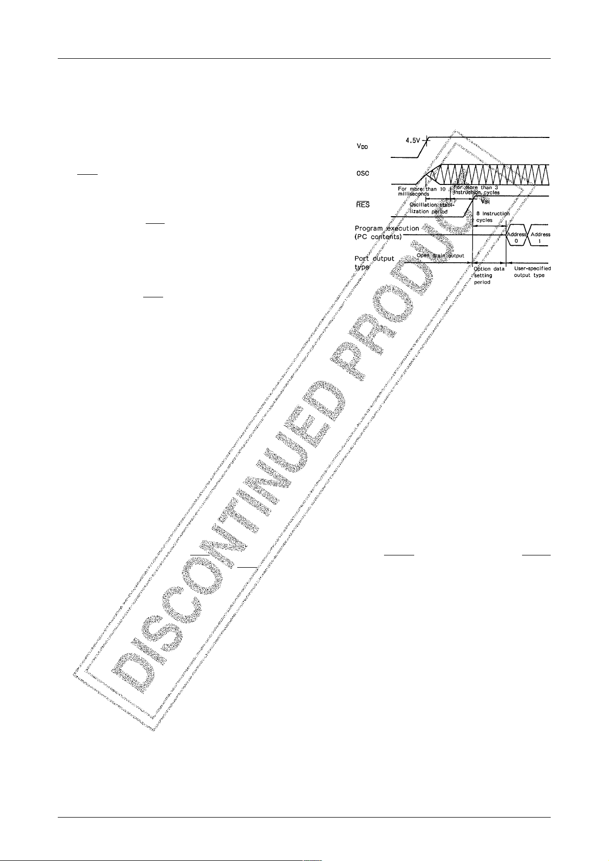
• Notes on LC66E516 internal operations after reset
As the figure shows, the LC66E516 microcontroller starts normal
program execution at least 3 instruction cycles later after the oscillation by the OSC function block becomes stable. In other words,
the RES pin level (active low) must be active for at least 3 instruction cycles after the oscillation becomes stabilized. As the figure
also shows, the oscillation stabilization requires more than 10 milliseconds. It is also shown that option data setting requires 8 instruction cycles after the RES pin level changes to the inactive level (or
voltage level). After all those operations are carried out, the
to V
IH
LC66E516 microcontroller starts program execution normally from
address 0 in the EPROM (that is, the content at address 0 is automatically set in the program counter (PC)). At this point, Please
note that port output type will be open-drain, not pull-up output
type, as long as the RES pin stays active.
• Notes on evaluation of user application programs for the LC66506, LC66508, LC66512, LC66556, LC66558, LC66562,
microcontrollers
The above six mask programmed ROM-version microcontrollers are equipped with different ROMs in size from that of
the LC66E516 microcontroller. Therefore, the following things should be taken into consider ation when you are to mak e
an access to the ROM on the LC66E516 microcontroller.
First, it should be kept in mind that the last 8 addresses between 3FF8 and 3FFF are used by the user in order to specify
functional option data. This 8-byte area is called option specification area. This option specification area must be exclusively used for storing function option data. The option specification will be discussed in detail later in this catalog.
As far as the cross assembler to be employed is concerned, the user should use the one for the LC66516 microcontroller.
In addition, when you write your user application program, you cannot make any access to addresses beyond the area of
a mask programmed ROM. Such addresses cannot exist an ywhere on mask programmed ROM-version microcontrollers.
T o avoid such an illegal access to those nonexistent area, it is recommended that jump (or branc h) operations with a JMP
instruction and so on be used in your user application program. Furthermore, please write "0" to the area beyond that of
a mask programmed ROM. In this case, needless to say, the last 8 addresses of the EPR OM should be e xcluded fr om the
"0" padding.
When evaluating the LC66506, LC66508, LC66556, LC66558, do not use the SB instruction.
• Program protection from exposure to light
Exposure to light will destroy the precious EPROM data that you ha v e entered with much labor. In order to protect them,
it should be strongly recommended that the EPROM window should be covered with an opaque label while you are at
work with the EPROM.
• For the LC66E516/P516, if the RES is set to "L" level during the HOLD mode (HOLD=L), be sure to change the HOLD
level from "L" to "H" and then change the RES level from "L" to "H" when releasing the HOLD mode.
No.2928–2/18
Page 3
LC66E516
Option-specified output type
“FFO
H
” is set.
4.0V to 6.0V/0.92 to 10
µs (tool:5V ±5%)
–30 to +70°C
2.5mA max.(4MHz ceramic resonator oscillation)
3.5mA max.(4MHz external clock source)
2.5mA max.(3MHz typ.RC oscillation)
(tool:evaluation impossible)
LC6655X series
65536 cycles
Approx. 64ms at 4MHz (Tcyc=1
µs)
16384 cycles
Approx. 32ms at 2MHz (Tcyc=2
µs)
Approx. 64ms at 1MHz (Tcyc=4
µs)
4.5V to 5.5V/0.92 to 10
µs
Open-drain output (other than P0, P1) (floating)
H/L output(P0, P1)with pull-up
“FFO
H
” is set.
65536 cycles
Approx. 64ms at 4MHz (Tcyc=1
µs)
LC665XX series(masked ROM version)
10 to 40°C
C=100pF
R=2.7kΩ(tool:R=2.2kΩ)
C=100pF
R=2.2kΩ
5.0mA max. (4MHz ceramic resonator oscillation)
6.0mA max. (4MHz external clock source)
5.0mA max. (3MHz typ. RC oscillation)
LC6650X series(including tool)
DIP64S
QFP64E
Not applicable
2.5mA max.(4MHz ceramic resonator oscillation)
3.5mA max.(4MHz external clock source)
DIP64S
QFP64A
LC66E516
Option-specified output type
“FFC
H
” is set.
DlC64S with window
QFC64 with window
2.2V to 5.5V/3.92 to 10
µs
3.0V to 5.5V/1.96 to 10
µs
Case outline (package)
• Port output type during reset
• Value(including the value after HOLD mode
release)of timer 0 during reset
Item
Differences in system
• Hardware wait time (number of cycles)at HOLD
mode released state
• External constants for RC oscillation
• Current drain during HALT mode ON (l
DD
HALT)
Differences in main characteristics
• Operating supply voltage/operating speed
• Operating free-air temperature (Topr)
Comparison of LC66E516 and the masked ROM version(LC665XX)
No.2928–3/18
Page 4
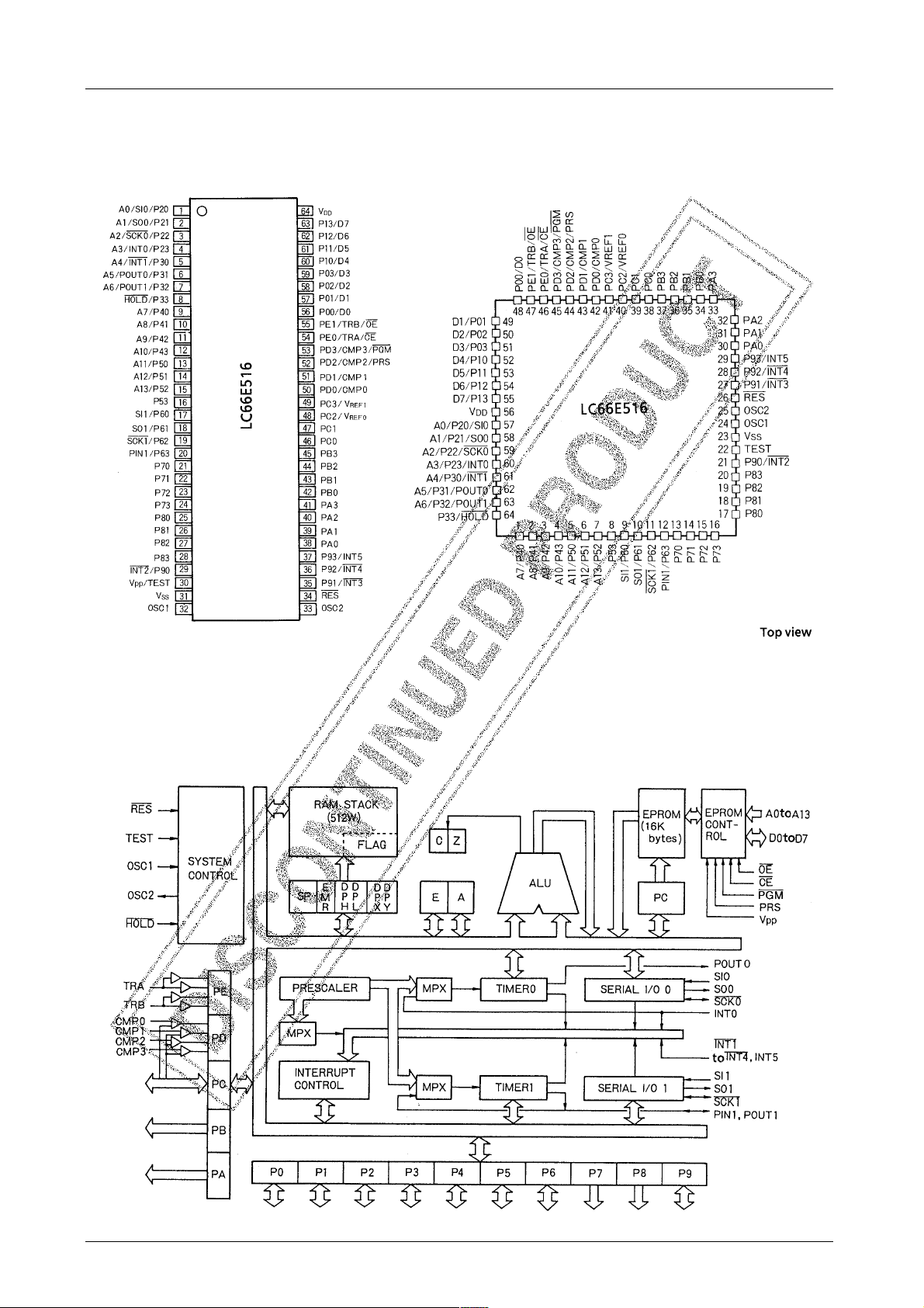
Pin Assignments
DIC64S with window QFC64 with window
LC66E516
Block Diagram
No.2928–4/18
Page 5
Pin Function
Pin name
P00/D0
P01/D1
P02/D2
P03/D3
P10/D4
P11/D5
P12/D6
P13/D7
P20/Sl0/A0
P21/SO0/A1
P22/SCK0/A2
P23/INT0/A3
LC66E516
Input/
output
Input/output port pins P00 to P03
I/O · Pch: Pull-up (Pu) MOS
· Used for input/output operation in 4-bit
units or bit units.
· Used for controlling HALT mode
operation.
Input/output port pins P10 to P13
I/O
· Used for input/output operation in 4-bit
units or bit units.
I/O
· Used for input/output operation in 4-bit
units or bit units.
· P20: Common with serial input SI0
P21: Common with serial output SO0
P22: Common with serial clock SCK0
· P23: Common with INT0 interrupt
request input, timer 0-used
event count input, pulse width
measurement input
Functional description
Input/output port pins P20 to P23
Output driver circuit
output type
type
· Nch: Small sink current
output type
· Pch: Pull-up (Pu) MOS
type
· Nch: Small sink current
output type
· Pch: CMOS type
· Nch: Small sink current
output type
· +15V withstand voltage at
Nch open drain (OD)
output
Option
· Pull-up (Pu) MOS
output type or Nch
open-drain (OD)
output type
· Output pin level at
reset
· Pu MOS output
type or Nch OD
output type
· Output pin level at
reset
· CMOS output type
or Nch OD output
type
During EPROM
mode operation
Data input/output
pins
(D0 to D3)
Data input/output
pins
(D4 to D7)
Address input
(A0 to A3)
P30/INT1/A4
P31/POUT0/A5
P32/POUT1/A6
P33/HOLD
P40/A7
P41/A8
P42/A9
P43/A10
P51/A12
P52/A13
P53
Input/output port pins P30 to P32
I/O
· Used for input/output operation in 3-bit
units or bit units and for input operation
in 4-bit units (together with the P33 pin)
or bit units.
· P30 : Common with INT1 interrupt
request input
· P31 : Common with burst pulse output
from timer 0
· P32 : Common with burst pulse output
from timer 1 and PWM output
I
HOLD mode control signal input
· Used for activating HOLD operation
mode with HOLD = L (active low) by
using a HOLD instruction.
· Used for restarting the CPU operation
from the HOLD mode operation by
changing the HOLD pin level from L to
H.
· Used as input port pin P33 to form a 4 bit input port with P30 to P32.
· The CPU blocks cannot be reset even if
the RES (active low) pin level changes
from H to L, with the HOLD pin level
= L. This means that you cannot write
a user application program requiring
the P33/HOLD pin to enter the L level
state at the moment the system is
powered on.
Input/output port pins P40 to P43
I/O
· Used for input/output operation in 4-bit
units or bit units.
· These four pins, combined with port
pins P50 to P53, can be used for
input/output operation in 8-bit units.
· These four pins, together with port pins
P50 to P53, can be used for 8-bit
ROM data output.
Input/output port pins P50 to P53
I/OP50/A11
· Used for input/output operation in 4-bit
units or bit units.
· These four pins, combined with port
pins P40 to P43, can be used for
input/output operation in 8-bit units.
· These four pins, together with port pins
P40 to P43, can be used for 8-bits ROM
data output.
· Pch: CMOS type
· Nch: Small sink current
output type
· +15V withstand voltage
for Nch OD output
· Pch: Pull-up (Pu) MOS
type
· Nch: Small sink current
output type
· Pch: Pull-up (Pu) MOS
type
· Nch: Small sink current
output type
· CMOS output type
or Nch OD output
type
· Pu MOS output type
or Nch OD output
type
· Pu MOS output type
or Nch OD output
type
Continued on next page.
Address input
(A4 to A6)
Address input
(A7 to A10)
Address input
(A11 to A13)
No.2928–5/18
Page 6
Continued from preceding page.
Pin name
P60/SI1
P61/SO1
P62/SCK1
P63/PIN1
Input/
output
I/O
LC66E516
Input/output port pins P60 to P63
· Used for input/output operation in 4-bit
units or bit units.
· P60: Common with serial input SI1
· P61: Common with serial output SO1
· P62: Common with serial clock SCK1
· P63: Common with timer 1-used event
count input
Output driver circuit
output type
· Pch: CMOS type
· Nch: Small sink current
output type
· +15V withstand voltage
for Nch OD output
OptionFunctional description
· CMOS output type
or Nch OD output
type
During EPROM
mode operation
P70
P71
P72
P73
P80
P81
P82
P83
P90/INT2
P91/INT3
P92/INT4
P93/INT5
PA0
PA1
PA2
PA3
PB0
PB1
PB2
PB3
PC0
PC1
PC2/VREF0
PC3/VERF1
Output port pins P70 to P73
O
· Used for output operation in 4-bit units or
in bit units.
· If you use an input-related instruction in
your application program, the content of
the output latch will be input.
Output port pins P80 to P83
O
· Used for output operation in 4-bit units or
bit units.
· If you use an input-related instruction in
your application program,the content of
the output latch will be read in.
· Pch OD output type optionally available.
More about this later.
Input/output port pins P90 to P93
I/O
· Used for input/output operation in 4-bit
units or bit units.
· P90: Common with INT2 interrupt request
input
· P91: Common with INT3 interrupt request
input
· P92: Common with INT4 interrupt request
input
· P93: Common with INT5 interrupt request
input
O
Output port pins PA0 to PA3
· Used for input operation in 4-bit units or bit
units.
· If you use an input-related instruction in
your application program, the content of
the output latch will be read in.
Output port pins PB0 to PB3
O
· Used for output operation in 4-bit units or
bit units.
· If you use an input-related instruction in
your application program, the content of
the output latch will be read in.
I/O
Input/output port pins PC0 to PC3
· Used for input/output operation in 4-bit
units or bit units.
· PC2: Common with VREF0 comparator
comparison voltage terminal
· PC3: Common with VREF1 comparator
comparison voltage terminal
· Pch: Pull-up (Pu) MOS
type
· Nch: Medium sink
current output type
· +15V withstand voltage
for Nch OD output type
· Pch: CMOS type
· Nch: Small sink current
type
· Pch: CMOS type
· Nch: Small sink current
type
· Pch: Pull-up (Pu) MOS
type
· Nch: Medium sink
current type
· +15V withstand voltage
for Nch OD output type
· Pch: Pull-up (Pu) MOS
type
· Nch: Medium sink
current type
· Pch: CMOS type
· Nch: Small sink current
type
· Pu MOS output type
or Nch output type
· CMOS output type
or Pch OD output
type
· Output pin level at
reset
· CMOS output type
or Nch OD output
type
· Pu MOS output type
or Nch OD output
type
· Pu MOS output type
or Nch OD output
type
· CMOS output type
or Nch OD output
type
PD0/CMP0
PD1/CMP1
PD2/CMP2/PRS
PD3/CMP3/PGM
PE0/TRA/CE
PE1/TRB/OE
Input port pins PD0 to PD3
I
· These four pins can be programmed for
comparator inputs in user application
programs. PD0 input will be compared
with VREF0. Other inputs will be
compared with VREF1. Please note that
there are four comparators available in this
system and these four comparators are
grouped into two (one group: CMP0 and
CMP1. the other group: CMP2 and CMP3),
and that the comparators must be selected
in group units.
I Input port pins PE0 to PE1
· These two tristate input port pins can be
controlled in your application programs.
EPROM control
signal inputs
(PRS and PGM)
EPROM controi
signal inputs
(OE and CE)
Continued on next page.
No.2928–6/18
Page 7

LC66E516
Continued from preceding page.
pin name
OSC1
OSC2
RES
TEST/V
V
DD
Vss
pp
Input/
output
Pins for connecting system clock oscillator
I
externally. If external clock source mode is
O
to be employed, use the OSC1 pin only for
clock input. Leave the other pin open.
Input port pin for system reset request
I
signal
· To initialize the CPU, the RES (active
low) pin level must be L with the P33/
HOLD pin level = H.
Input port pin for CPU test signal
I
This pin should be connected with the
VSS pin when this device is in operation.
Power supply pin
Functional description
Remarks:
Pu MOS type output --- Pch MOS type transistor acts as a pull-up resistor when data is output.
CMOS type output --- Pch MOS type transistor does not act as a pull-up resistor when data is output.
Instead, it forms a complementary-symmetry MOS output circuit with an Nch MOS type
transistor.
OD output --- Open drain output type
Note:
At the system reset, the pin output level of each of input/output and output port pins will be "H" except for such pins as
ports 0, 1 and 8. The output level of these e xceptions can be specified by the user options. In addition to this system reset
operation, the port output type will be set to open drain at the system reset, which is irrespective of user option specification. In this case, there is no exception.
User options
1. Option for specifying the output level of ports 0, 1 and 8 at the system reset
The output level of ports 0, 1 and 8 at the system reset can be selected from the following two optional levels by the
user option. In this case, it should be kept in mind that the output levels of all the four bits of each input/output port are
specified at the same time.
Option name
1. "H" output level
Output driver circuit
output type
Condition
In 4-bit units
In 4-bit units2. "L" output level
Option
· Ceramic resonator
oscillation. RC
oscillation or
external clock
source
During EPROM
mode operation
2. Option for selecting oscillation circuit
Option name Selectable oscillation circuit
1. External clock source
OSC2) RC oscillation
circuit
3. Ceramic resonator
oscillation circuit
Condition
· Schmitt trigger input
· Schmitt trigger input2. 2-pin (OSC1 and
No.2928–7/18
Page 8

LC66E516
3. Option for selecting watchdog timer function
This option permits the user to select the watchdog timer function. This function could be helpful in detecting a
timeout error from your user application program.
4. Option for specifying port output type
i) This option permits the user to select a desired port output type of the following ports from the two output types listed
in the table below. Please note that port output types can be specified in bit units.
Ports: P0, P1, P2, P3 (P33/HOLD not included), P4, P5, P6, P7, P9, PA, PB, and PC
Selected output circuit typeOption name Condition
1. Open drain output
type
Ports P7, PA and PB are provided exclusively for output operation.
Ports P2, P3, P6 and P9 employ Schmitt trigger input.
2. Pull-up transistor
output type
Ports P7, PA and PB are provided exclusively for output operation.
Ports P2, P3, P6 and P9 employ Schmitt trigger input.
The Pch type MOS transistor can act as either a pull-up resistor (for
Pu MOS output circuit) or an output transistor (CMOS output circuit),
which depends on its driving capability.
CMOS output type: P2, P3, P6, P9 and PC.
Pu MOS output: P0, P1, P4, P5, P7, PA and PB.
ii) The output type of P8 can be selected from the following two options. Please note that the output types for the por t pins
can be specified in bit units.
Selected output circuit typeOption name Condition
1. Option drain output
type (Pch OD)
2. Pull-down resistor
output type
iii) Comparator input of the PD and tristate input of the PE can be specified in your user application program.
User option specification
To select desired user options, you must write appropriate data into the user option specification area in the on-chip
EPROM. The user option specification will be discussed in detail on the following pages.
No.2928–8/18
Page 9

LC66E516
How to write data in the user option specification area and the program area in the on-chip EPROM
(1) Writing option codes to the user option specification area
Use the cross assembler for the LC66516 mask programmed ROM-version microcontroller when you write option
codes in the user specification area. When your source application program is assembled, the option data will be
stored in the user option specification area (3FF8 through 3FFF). In addition to the above writing , you are allowed to
write option data directly into the user option specification area in the on-chip EPROM. In this case, making references to the option code specification list on the next page will be a "must".
(2) Writing program into the on-chip EPROM program area
An EPROM writer available on your local market can be used to write program into the on-chip EPROM program
area. In this case, the EPROM writer (27128 EPROM writer) must be used together with the dedicated writer board
because the pin conversion (64 into 28) is required. The dedicated writer board is shown below.
Please note that the EPROM writer must be either an ADVANTEST product or the EVA800/850 accessory writer.
Such an EPROM writer enables you to write your application program into the EPROM in Intel high-speed writing
method.
ModelManufacturer
This dedicated writer board is inserted into
ADVANTEST
TR4943, R4944A, R4945 or equivalent
the EPROM writer available on your local
market. (Select either an ADVANTEST
writer product or the EVA800/850 acces-
SANYO
EVA850 or EVA800 accessory
EPROM writer
sory EPROM writer).
Notes
1. Intel is a registered trademark of Intel Corporation.
2. ADVANTEST is a registered trademark of
ADVANTEST Corporation.
(3) How to erase the contents of the on-chip EPROM
To erase the contents of the on-chip EPROM, you can use an EPROM eraser available on your local market.
No.2928–9/18
Page 10

Option code specification list
LC66E516
ROM address
3FF8H
3FF9H
3FFAH
3FFBH
3FFCH
3FFDH
3FFEH
3FFFH
Bit
7
6
5
4
3
2
1
0
7
6
5
4
3
2
1
0
7
6
5
4
3
2
1
0
7
6
5
4
3
2
1
0
7
6
5
4
3
2
1
0
7
6
5
4
3
2
1
0
7
6
5
4
3
2
1
0
7
6
5
4
3
2
1
P8
P1
P0
P13
P12
P11
P10
P03
P02
P01
P00
P33
P32
P31
P30
P23
P22
P21
P20
P53
P52
P51
P50
P43
P42
P41
P40
P73
P72
P71
P70
P63
P62
P61
P60
P93
P92
P91
P90
P83
P82
P81
P80
PB3
PB2
PB1
PB0
PA3
PA2
PA1
PA0
PC3
PC2
PC1
PC00
Optional item
Unused
Oscillation circuit type
Output level at the
system reset
Watchdog timer function option
Output circuit type
Output circuit type
Unused
Output circuit type
Output circuit type
Output circuit type
Output circuit type
Output circuit type
Output circuit type
Output circuit type
Output circuit type
Output circuit type
Output circuit type
Unused
Output circuit type
1: Ceramic resonator oscillation. 0: RC oscillation or external clock source
Option data and selections
Always set to "0".
1="H"–level, 0="L"–level
1: Selected. 0: Not selected.
1=PU, 0=OD
1=PU, 0=OD
Always set to "0".
1=PU, 0=OD
1=PU, 0=OD
1=PU, 0=OD
1=PU, 0=OD
1=PU, 0=OD
1=PU, 0=OD
1=PU, 0=OD
1=PD, 0=OD
1=PU, 0=OD
1=PU, 0=OD
Always set to "0".
1=PU, 0=OD
Remarks:
PU --- Pull-up MOS type resistance output
PD --- Pull-down MOS type resistance output
OD --- Open-drain output
Note: The pull-up MOS type resistance output represents the pull-up MOS (Pu MOS) type resistor output circuit and the
complementary MOS (CMOS) type output circuit.
No.2928–10/18
Page 11

LC66E516
Specifications
Absolute Maximum Ratings at Ta = 25˚C, VSS=0V
Supply voltage
Input voltage
Output voltage
Output current per
pin
Pin total current
Symbol
V
DD
VIN(1)
VIN(2)
V
(1)
OUT
V
(2)
OUT
ION(1)
ION(2)
–IOP(1)
∑ION(1)
∑ION(2)
–∑IOP(1)
Pins applicable and related
information
V
DD
P2, P3 (except P33/HOLD)
and P6.
All the pins other than the
above
P2,P 3 (except P33/HOLD),
P6, P7 and PA.
All the pins other than the
above.
P0, P1, P2, P3 ( except
P33/HOLD), P4, P5, P6,P8,P9
and PC.
P7, PA, PB
P0, P1, P4, P5, P7, PA, PB
P2, P3 (except P33/HOLD),
P6, P8, P9 and PC.
P2, P3 (except P33/HOLD),
P4, P5, P6, P7 and P8.
P0, P1, P9, PA, PB, PC
P2, P3 (except P33/HOLD),
P4, P5, P6, P7 and P8.
Conditions
Ratings
–0.3 to +7.0
–0.3 to +15.0
–0.2 to VDD+0.3
–0.3 to +15.0
–0.3 to VDD+0.3
Unit
V
V
V
V
V
4
mA
20
mA
2
mA
4–IOP(2)
mA
75
mA
75
mA
25
mA
NoteParameter
1
2
1
2
3
3
4
4
3
3
4
Allowable power
dissipation
Operating
temperature
–∑IOP(2)
Pd max
Topr 10 to 40 °C
Tstg °C–55 to +125Storage temperature
P0, P1, P9, PA, PB, PC
Ta=10 to 40°C DIC-64S
600
25
mA
mW
4
Note 1: Applicable only to the pins with open drain output circuit. Otherwise, refer to the values listed in the "all the pins
other than the above" column.
Note 2: As far as oscillation input and output are concerned, the voltage range can cover the self-oscillating level.
Note 3: Sink current. As far as the P8 is concerned, these parameters can apply only to the CMOS output circuit.
Note 4: Source current. Apply to the both of the pull-up output circuit and the CMOS output circuit except for P8.
Allowable operating conditions at Ta = 10˚C to 40°C, V
Parameter
Operating supply
voltage
Memory backup
voltage
Input high-level
voltage
symbol
V
DD
VDD(H)
VIH(1)
VIH(2)
VIH(3)
VIH(4) PE
V
DD
V
DD
P2, P3(except P33/
HOLD) and P6.
P33/HOLD, P9
RES
OSC1
PO, P1, P4, P5, PC,
PD, PE
ConditionsPins applicable
With HOLD mode
"ON"
With output Nch
transistor "OFF"
With output Nch
transistor "OFF"
With output Nch
transistor "OFF"
With tristate input
mode selected
=0V, unless otherwise noted
SS
4.5
1.8
4.5 to 5.5
4.5 to 5.5
4.5 to 5.5
4.5 to 5.5
0.75V
0.75V
0.7V
0.8V
DD
DD
DD
DD
Ratings
typVDD(V) min max
5.0
Unit
Note
5.5
V
5.5
V
+13.5
V
DD
V
DD
V
DD
1
V
2
V
3
V
V
Continued on next page.
No.2928–11/18
Page 12

Continued from preceding page.
LC66E516
Parameter
Intermediate level
input voltage
In-phase input
voltage
Input low-level
voltage
Operating frequency
(instruction cycle
time)
Frequency
Pulse width
External clock input modeself oscillation mode
Rise and Fall
times
Oscillation
frequency
Oscillation
stabilization
Ceramic resonator
oscillation
time period
External R and
C constants
Symbol
V
IM
V
CMM
VIL(1)
VIL(2)
VIL(3)
VIL(4)
fop
(TCYC)
fext
textH
textL
textR
textF
f
CF
CFS
Cext
Rext
ConditionsPins applicable
PE
PD, PC2, PC3 4.5 to 5.5
P2, P3(except P33/
HOLD), P6, P9 and
RES.
OSC1
P33/HOLD
P0, P1, P4, P5, PC, PD,
PE, TEST
PE
OSC1
OSC1, OSC2
OSC1, OSC2
With tristate input
mode selected.
With comparator
input mode selected
With output Nch
transistor "OFF"
With output Nch
transistor "OFF"
With tristate input mode
selected.
Please refer to Figure 1.
As it shows, input clocks
reach the OSCl pin from
an external clock source
and the OSC2 pin should
be left open. The oscil-
lation circuit option
should be "external clock
input".
Please refer to Figure 1.
As it shows, input clocks
reach the OSC1 pin from
an external clock source
and the OSC2 pin should
be left open. The oscil-
lation circuit option
should be "external clock
input".
Please refer to Figure 1.
As it shows, input clocks
reach the OSC1 pin from
an external clock source
and the OSC2 pin should
be left open. The oscil-
lation circuit option
should be "external clock
input".
Refer to
Figure 2.
Refer to
Figure 3
Refer to Figure 4
4MHz 4.5 to 5.5t
VDD(V)
4.5 to 5.5
4.5 to 5.5 Vss
1.8 to 5.5
4.5 to 5.5
4.5 to 5.5
4.5 to 5.5
4.5 to 5.5
4.5 to 5.5
4.5 to 5.5
4.5 to 5.54MHz
4.5 to 5.5
Ratings
min typ max
0.4V
DD
1.0
Vss
Vss
Vss
0.4
(10)
0.4
70
0.6V
VDD–l.5
0.25V
0.25V
0.3V
0.2V
4.0
100
2.2
DD
DD
DD
DD
DD
4.35
(0.92)
4.35
30
10
Unit
V
V
V2
V
V3
V
MHz
(µs)
MHz
ns
ns
MHz
ms
pF
kΩ
Note
Note 1: These values apply to the case where the open-drain circuit type has been specified. Note that the P33/HOLD pin
is not included (refer to the values listed in V
(2) column and that the pins P2, P3 and P6 cannot be used as the
IH
input pins as far as the CMOS output circuit type has been employed.
Note 2: These values apply to the case where the open drain circuit type has been selected. Note that the pin P9 cannot be
used as the input pin as far as the CMOS type output circuit has been employed.
Note 3: When the pin PE has been selected as the tristate input pin, the values listed in the V
(4), VIM and VIL(4) columns
IH
should apply to the pin. Note that the pin PC cannot be used as the input pin as far as the CMOS type output circuit
has been employed.
No.2928–12/18
Page 13

LC66E516
Electrical chracteristics at Ta = 10˚C to 40°C, VSS=0V, unless otherwise noted
Parameter Symbol
Input high-level
current
Input low-level
current
Output high-level
voltage
Output pull-up
current
Output low-level
voltage
Output-OFF
leakage current
Comparator offset
current
IIH(2)
IIH(3)
IIL(1)
IIL(2)
VOH(1)
VOH(2)
I
PO
VOL(1)
VOL(2)
I
OFF
I
OFF
I
OFF
V
OFF
Pins applicable
P2, P3(except P33/
HOLD) and P6.
P0, P1, P4, P5, P9, PC,
OSC1, RES and P33/
HOLD.
Note that the PD, PE,
PC2, and PC3 are not
included.
PD, PE, PC2, PC3
Input pins otner than
PD, PE, PC2 and PC3
PC2, PC3, PD, PE
P2, P3(except P33/
HOLD), P6, P8, P9, and
PC.
P0, P1, P4, P5, P7, PA,
PB
P0, P1, P4, P5, P7, PA,
PB
PO, P1, P2, P3, P4, P5,
P6, P8, P9 and PC
(except P33/ HOLD).
P7, PA, PB
(1)
P2, P3, P6, P7, PA
Pins other than P2, P3,
(2)
P6, P7, P8 and PA
(3)
P8
PD
Conditions
VIN = 13.5V
With output Nch
transistor "OFF"
VIN = V
DD
With output Nch
transistor "OFF"
VIN = V
DD
With output Nch
transistor "OFF"
VIN = Vss
With output Nch
transistor "OFF"
VIN = Vss
With output Nch
transistor "OFF"
IOH = –1mA
IOH = –0.1mA
I
= –200µA
OH
I
= –130µA
OH
VIN = Vss
IOL = 1.6mA
IOL = 10mA
VIN = 13.5V
VIN = V
DD
VIN = 1.0V to
VDD–l.5V
VDD(V)
4.5 to 5.5
4.5 to 5.5
4.5 to 5.5
4.5 to 5.5
4.5 to 5.5
4.5 to 5.5
4.5 to 5.5
4.5
4.5 to 5.5
5.5
4.5 to 5.5
4.5 to 5.5
4.5 to 5.5
4.5 to 5.5
4.5 to 5.5 –1.0VIN = Vss
4.5 to 5.5
min
VDD–1.0
VDD–0.5
VDD–1.35
–1.0
–1.0
2.4
–1.6
Ratings
±50
Unit
µA
µA
µA
µA
µA
V
V
V
V
mA
V
V
µA
µA
µA
mV
Note
1
1
1
2
2
3
3
4
4
4
5
6
6
7
maxtyp
5.0IIH(1)
1.0
1.0
0.4
1.5
5.0
1.0
±300
Hysteresis
voltage
High-level
threshold
voltage
Low-level
threshold
Schmitt characteristics
voltage
RC oscillation
frequency range
V
Vt H
Vt L
HYS
P2, P3, RES, P6, P9,
OSC1 (RC, EXT)
f
OSC1, OSC2
RC
Refer to Figure 4.
C =100pF ±5%
R = 2.2kΩ ±1%
4.5 to 5.5
0.5V
DD
0.25V
DD
2.04.5 to 5.5 3.0
0.1V
DD
0.75V
DD
0.5V
DD
4.0
Continued on next page.
V
V
V
MHz
No.2928–13/18
Page 14

Continued from preceding page.
LC66E516
Parameter
Cycle time
Low-level
and highlevel pulse
width
Rise and
fall time
Data setup time
Data HOLD
Serial input Serial timing clock
time
Output delay
time
Data
input
Data
output
Data
input
Data
output
Data
output
symbol
t
CKCY
tCKL
tCKH
t
CKR
t
CKF
t
ICK
t
CKI
t
CKO
Pins applicable
SCK0, SCK1
SI0, SI1
SO0, SO1
Conditions
Refer to Figure 5
(timings) and Figure6
(test load).
Refer to Figure 5
(timings).
Time periods based
on the SCK0 and
SCK1 clock rising
edges(↑).
Refer to Figure 5
(timings) and Figure 6
(test load).
Time period based on
the SCK0 and SCK1
clock falling edges(↓).
4.5 to 5.5
4.5 to 5.5
4.5 to 5.5
4.5 to 5.5
4.5 to 5.5
4.5 to 5.5
4.5 to 5.5
4.5 to 5.5
Ratings
min typVDD(V)
0.9
2.0
0.4
1.0
0.3
0.3
max
0.1
0.3
Unit
T
T
Note
µs
CYC
µs
CYC
µs
µs
µs
µs
INT0 high-level
and low-level
pulse width
High-level and
low-level pulse
width (INTO
not included)
Pulse input conditions Serial output
PIN1 high-level
and low-level
pulse width
RES high-level
and low-level
pulse width
Comparator
response speed
Current drain during
basis operation
mode
t
I0H
t
I0L
t
I1H
t
I1L
t
PINH
t
PINL
t
RSH
t
RSL
T
RS
I
DD OP
INT0
INT1, INT2,
INT3, INT4,
INT5
PIN1
RES
PD
V
DD
· With INTO interrupt
request input
acceptable.
· With event counter
(timer 0) input or
pulse width
measuring input
acceptable.
Refer
to
· With interrupt
Figure
request inputs
7.-
acceptable
·With event counter
(timer 1) input
acceptable
· With reset request
acceptable
Refer
to
Figure
8.
4 MHz ceramic
resonator oscillation
4 MHz external clock
source
RC oscillation
4.5 to 5.5
4.5 to 5.5
4.5 to 5.5
2
2
2
3
4.5
6.5
T
CYC
T
CYC
T
CYC
T
CYC
30
µs
8
mA
mA
mA4.0 8
8
11
Continued on next page.
No.2928–14/18
Page 15

Continued from preceding page.
LC66E516
Parameter Unit
Current drain during
HALT operation
mode
Current drain during
HOLD operation
mode
symbol
I
DDHALTVDD
I
DDHOLD
Pin applicable
V
DD
Conditions
4 MHz ceramic
resonator oscillation
4 MHz external clock
source
RC oscillation
VDD(V)
4.5 to 5.5
1.8 to 5.5 0.01
Limits
typ
2.5
3.5
2.5
maxmin
4.5
6.0
4.5
10 µA
Note
mA
mA
mA
Note 1: Applicable to the case where input/output common ports have been set to open-drain output circuit type and the
output Nch transistors have been in OFF state. Note that the input/output common ports cannot be used as the
input port if they have been set to the CMOS output circuit type.
Note 2: Applicable to the case where input/output common ports have been set to open-drain output circuit type and the
output Nch transistors have been in OFF state. If the pull-up transistor output circuit type has been employed,
please refer to the value listed in the output pull-up current column (IPO). Note that input/output common ports
cannot be used as the input ports if they have been set to the CMOS output circuit type.
Note 3: Applicable to the case where the ports ha ve been set to the CMOS output circuit type and the output Nc h transistors
have been in OFF state. Also applicable to the P8 pin as far as it has been set to the Pch open-drain output circuit
type.
Note 4: Applicable to the case where the ports have been set to the pull-up resistor output circuit type and the output Nch
transistors have been in OFF state.
Note 5: Applicable to the case where the P8 pin has been set to the CMOS output circuit type.
Note 6: Applicable to the case where the ports have been set to the open-drain output circuit type and the output Nch
transistors have been in OFF state.
Note 7: Applicable to the case where the port has been set to the open-drain output circuit type and the output Pch transistor
has been in OFF state.
Note 8: Reset mode.
Figure 1. External clock input waveform
Figure 2. Ceramic resonator oscillation circuit Figure 3. Oscillation stabilization time
No.2928–15/18
Page 16

33pF±10%
4 MHz (Murata)
CSA4.00MG
4 MHz (Kyocera)
Capacitance
(external)
KBR4.0MS
4 MHz (Murata) CST4.00MG
4 MHz (Kyocera) KBR–4.0MES
Capacitance
(internal)
C1
C2
C1
C2
33pF±10%
33pF±10%
33pF±10%
Table 1. Ceramic resonator oscillation constants
(recommended)
LC66E516
Figure 4. RC oscillation
Figure 6. Timing load
Figure 5. Serial input/output timings
Figure 7. Input timings for INT0, INT1, INT2, INT3, INT4, INT5, PIN1 and RES
No.2928–16/18
Page 17

LC66E516
Figure 8. Comparator response speed (TRS) and output timing
LC66E516 RC oscillation characteristics
Figure 9 shows the RC oscillation characteristics of the LC66E516 microcontroller.
The RC oscillation frequency range that can be guaranteed is shown below with the external constants and other conditions:
<
2.0MHz fRC 4.0MHz
<
=
=
External constants --- Cext = 100pF and Rext = 2.2kΩ
Ta = 10°C to 40°C and V
= 4.5V to 5.5V
DD
If you are to employ the external constants other than the above, the Rext and the Cext should be within the range between
T.B.D kΩ and T.B.D kΩ, and between T.B.D pF and T.B.D pF, respectively. Please take a close look at the figure below.
Note 10: With V
= 4.5V to 5.5V and Ta = 10°C to 40°C, the oscillation frequency to be selected should meet the
DD
requirement that the operating frequencies in the range between 0.4MHz and 4.3MHz must be provided without fail.
Figure 9. RC oscillation frequency reference values
No.2928–17/18
Page 18

Series Lineup
LC66E516
Type Number
LC66304A/306A/308A
LC66404A/406/408A
LC66506B/508B/512B/516B
LC66354A/356A/358A
LC66354S/356S/358S
LC66556A/558A/562A/566A
LC66354B/356B/358B
LC66556B/558B
LC66562B/566B
LC66E308
LC66P308
LC66E408
LC66P408
LC66E516
*
Pins PackageROM capacity
4K/6K/8KB 512W DIP42S QFP48E42
4K/6K/8KB
42
6K/8K/12K/16KB
64
42
4K/6K/8KB
4K/6K/8KB
42
64
6K/8K/12K/16KB
42
4K/6K/8KB
64
6K/8KB
64
12K/16KB
42
EPROM 8KB
OTPROM 8KB
42
EPROM 8KB 512W
42
42
EPROM 16KB
64
RAM cap
512W
512W
512W
512W
512W
512W
512W
512W
512W
512W
512WOTPROM 8KB
512W DIC64S
DIP42S QFP48E
DIP64S QFP64A
DIP42S QFP48E
QFP44M
DIP64S QFP64E
DIP42S QFP48E
DIP64S QFP64E
DIP64S QFP64E
DIC42S
DIP42S QFP48E
DIC42S
DIP42S QFP48E
QFC48
*
QFC48
*
QFC64
*
Features
Normal version
4.0 to 6.0V/0.92µs
Low voltage version
2.2 to 5.5V/0.92µs
Low voltage high-speed
version 3.0 to 5.5V/0.92µs
*
Evaluation-use windowed
version & one-time version
4.5 to 5.5V/0.92µs
*
:with window
*
*
64LC66P516 OTPROM 16KB
512W
DIP64S QFP64E
*Note : Under develoment
Specifications of any and all SANYO products described or contained herein stipulate the performance,
characteristics, and functions of the described products in the independent state, and are not guarantees
of the performance, characteristics, and functions of the described products as mounted in the customer's
products or equipment. To verify symptoms and states that cannot be evaluated in an independent device,
the customer should always evaluate and test devices mounted in the customer's products or equipment.
SANYO Electric Co., Ltd. strives to supply high-quality high-reliability products. However, any and all
semiconductor products fail with some probability. It is possible that these probabilistic failures could
give rise to accidents or events that could endanger human lives, that could give rise to smoke or fire,
or that could cause damage to other property. When designing equipment, adopt safety measures so
that these kinds of accidents or events cannot occur. Such measures include but are not limited to protective
circuits and error prevention circuits for safe design, redundant design, and structural design.
In the event that any or all SANYO products(including technical data,services) described or
contained herein are controlled under any of applicable local export control laws and regulations,
such products must not be exported without obtaining the export license from the authorities
concerned in accordance with the above law.
No part of this publication may be reproduced or transmitted in any form or by any means, electronic or
mechanical, including photocopying and recording, or any information storage or retrieval system,
or otherwise, without the prior written permission of SANYO Electric Co. , Ltd.
Any and all information described or contained herein are subject to change without notice due to
product/technology improvement, etc. When designing equipment, refer to the "Delivery Specification"
for the SANYO product that you intend to use.
Information (including circuit diagrams and circuit parameters) herein is for example only ; it is not
guaranteed for volume production. SANYO believes information herein is accurate and reliable, but
no guarantees are made or implied regarding its use or any infringements of intellectual property rights
or other rights of third parties.
This catalog provides information as of October, 2001. Specifications and information herein are subject
to change without notice.
No.2928–18/18
 Loading...