

Page 1

Ordering number : EN4677
93098HA (OT) / 83194TH (OT) B8-0696 No. 4677-1/23
LC66354B, 66356B, 66358B
SANYO Electric Co.,Ltd. Semiconductor Bussiness Headquarters
TOKYO OFFICE Tokyo Bldg., 1-10, 1 Chome, Ueno, Taito-ku, TOKYO, 110-8534 JAPAN
Four-bit Single-Chip Microcontrollers
On-Chip 4 K/6 K/8 K-byte ROM
CMOS LSI
Any and all SANYO products described or contained herein do not have specifications that can handle
applications that require extremely high levels of reliability, such as life-support systems, aircraft’s
control systems, or other applications whose failure can be reasonably expected to result in serious
physical and/or material damage. Consult with your SANYO representative nearest you before using
any SANYO products described or contained herein in such applications.
SANYO assumes no responsibility for equipment failures that result from using products at values that
exceed, even momentarily, rated values (such as maximum ratings, operating condition ranges, or other
parameters) listed in products specifications of any and all SANYO products described or contained
herein.
Overview
The LC66354B, LC66356B and LC66358B are 42-pin
package four-bit CMOS microcontrollers that integrate on
a single chip all functions required in a control
microcontroller, including ROM, RAM, I/O ports, serial
interfaces, comparator inputs, three-value inputs, timers
and an interrupt system. These products differ from the
earlier LC66358A series in their power supply voltage
range and operating speed specifications.
Features and Functions
• ROM (with 4 K-, 6 K- and 8 K-byte capacities) and
RAM (512 4-bit digits) on chip
• LC66000 series compatible instruction set
(128 instructions)
• A total of 36 I/O port pins
• Two eight-bit serial interfaces that can be connected in
cascade to form a 16-bit interface
• Instruction cycle time: 0.92 to 10 µs (3 to 5.5 V)
The earlier LC66358A series had instruction cycle times
of from 1.96 to 10 µs (at 3 to 5.5 V) and from 3.92 to
10 µs (at 2.2 to 5.5 V).
• Powerful timer and prescaler functions
Time limit timer, event counter, pulse width measurement
and square wave output using a 12-bit timer.
Time limit timer, event counter, PWM output and
square wave output using an 8-bit timer.
Time base function using a 12-bit prescaler.
• Powerful interrupt system with eight interrupts and eight
vector locations
External interrupts: three interrupts and three vector
locations
Internal interrupts: five interrupts and five vector
locations
• Flexible I/O functions
Comparator inputs, three-value inputs, 20 mA drive
outputs, 15 V withstand voltage, pull-up or open-drain
option switching
• Runaway detection function (watchdog timer) option
• Eight-bit I/O function
• Power reduction functions using halt and hold modes
• Packages: DIP42S, QIP48E (QFP48E)
• Evaluation LSI: used together
— LC66599 (evaluation chip) + EVA850/800-
TB6630X
— LC66E308 (on-chip EPROM microcontroller)
Page 2
Series Structure
Note: * Under development
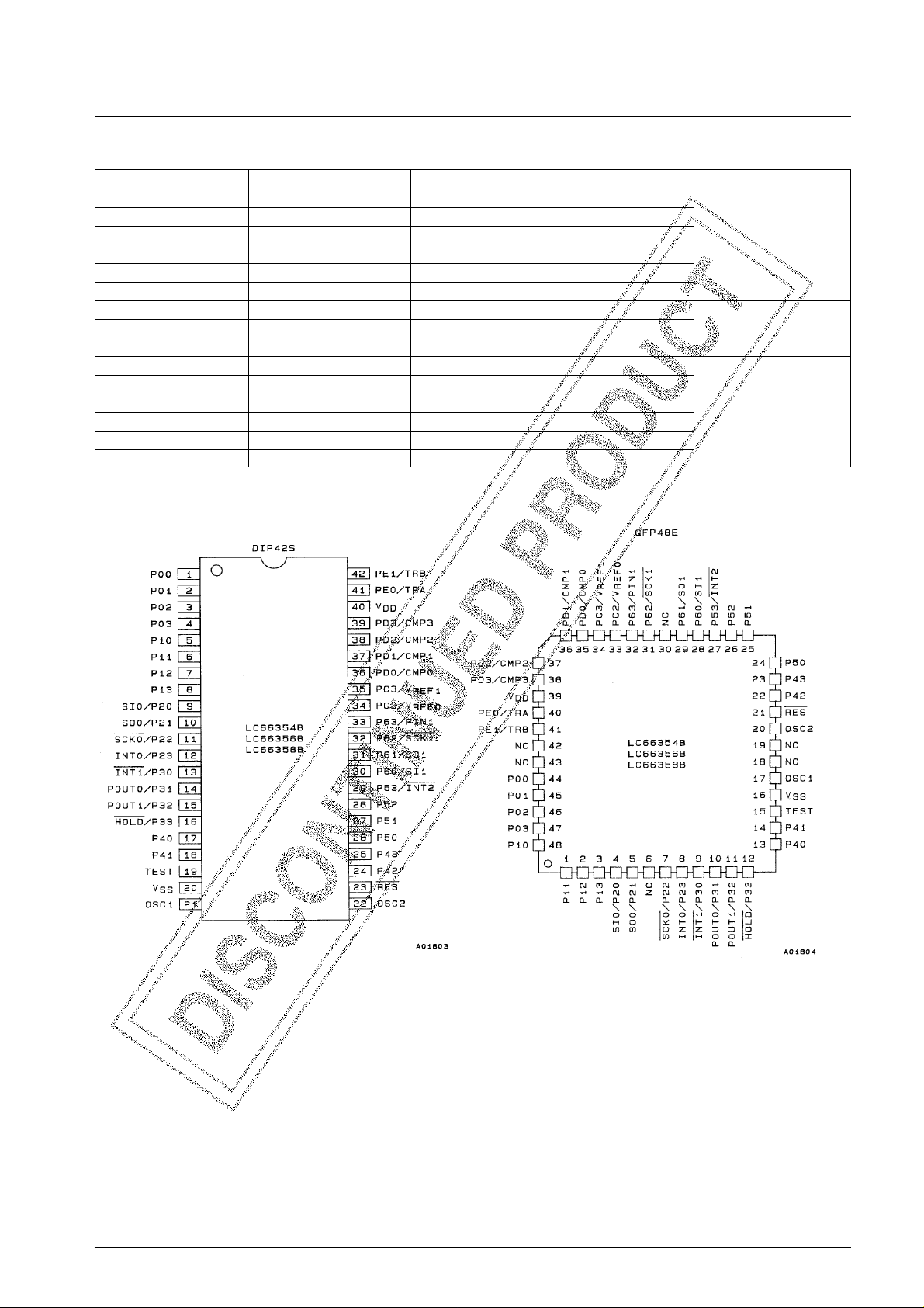
Pin Assignments
We recommend using reflow soldering methods to mount the QFP package version.
Contact your Sanyo sales representative to discuss process conditions if techniques in which the whole package is
immersed in a solder bath (solder dip or spray techniques) are used.
No. 4677-2/23
LC66354B, 66356B, 66358B
Product name Pins ROM capacity RAM capacity Package Features
LC66304A/306A/308A 42, 48 4 K/6 K/8 K bytes 512 W DIP42S QFP48E
Normal version
LC66404A/406A/408A 42, 48 4 K/6 K/8 K bytes 512 W DIP42S QFP48E
4.0 to 6.0 V/0.92 µs
LC66506B/508B/512B/516B 64 6 K/8 K/12 K/16 K bytes 512 W DIP64S QFP64A
LC66354A/356A/358A 42, 48 4 K/6 K/8 K bytes 512 W DIP42S QFP48E
Low-voltage version
LC66354S/356S/358S
*
44 4 K/6 K/8 K bytes 512 W QFP44M
2.2 to 5.5 V/3.92 µs
LC66556A/558A/562A/566A 64 6 K/8 K/12 K/16 K bytes 512 W DIP64S QFP64E
LC66354B/356B/358B 42, 48 4 K/6 K/8 K bytes 512 W DIP42S QFP48E
Low-voltage, high-speed
LC66556B/558B
*
64 6 K/8 K bytes 512 W DIP64S QFP64E version
LC66562B/566B 64 12 K/16 K bytes 512 W DIP64S QFP64E
3.0 to 5.5 V/0.92 µs
LC66E308 42, 48 EPROM, 8 K bytes 512 W DIC42S (window) QFC48 (window)
LC66P308 42, 48 OTPROM, 8 K bytes 512 W DIP42S QFP48E
LC66E408 42, 48 EPROM, 8 K bytes 512 W DIC42S (window) QFC48 (window)
Evaluation window and OTP
LC66P408 42, 48 OTPROM, 8 K bytes 512 W DIP42S QFP48E
versions
LC66E516 64 EPROM 16 K bytes 512 W DIC64S (window) QFC64 (window)
4.5 to 5.5 V/0.92 µs
LC66P516 64 OTPROM 16 K bytes 512 W DIP64S QFP64E
Top view
Page 3
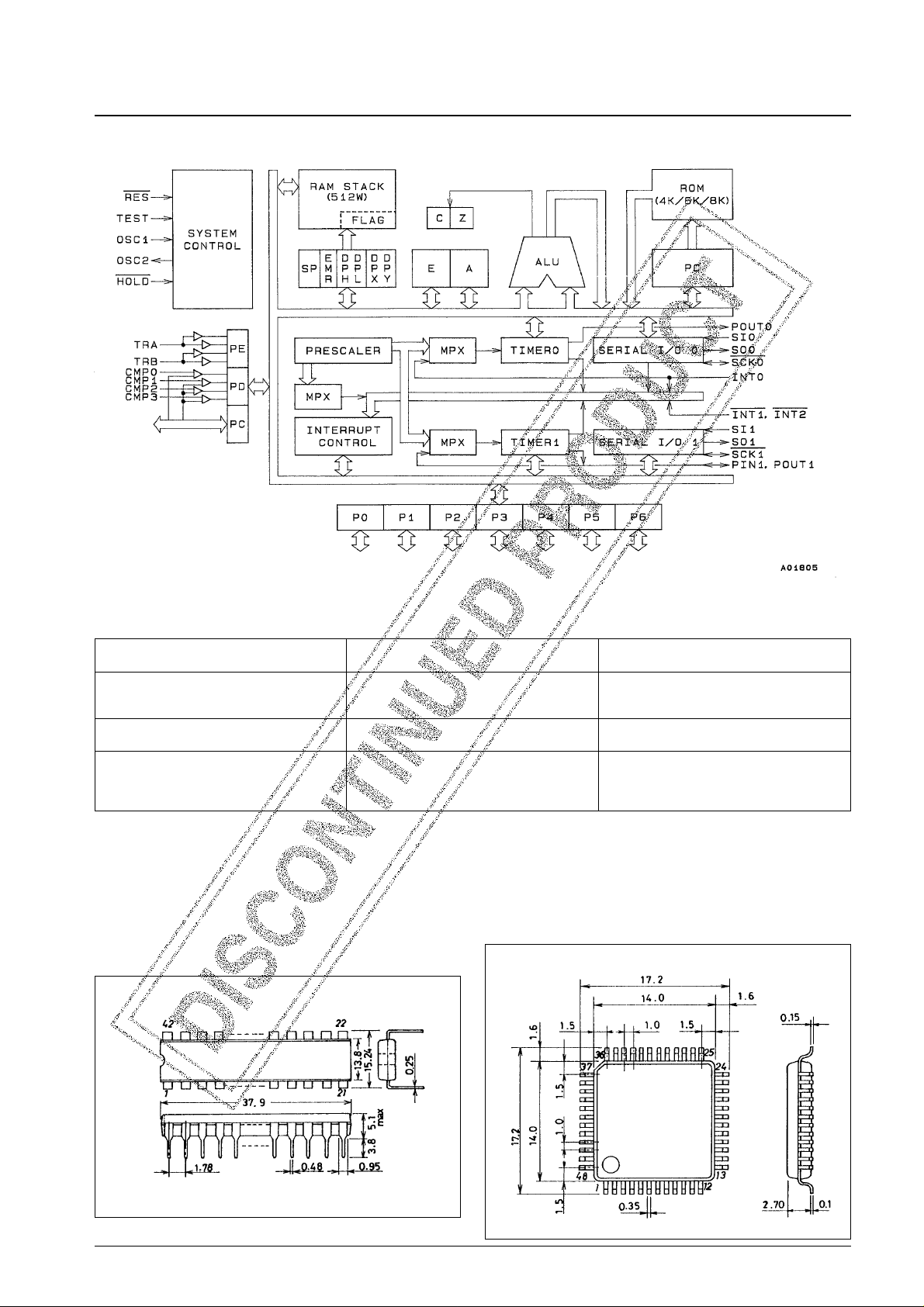
System Block Diagram
Differences between the LC66354B, LC66356B and LC66358B and the LC6630X Series
Note: 1. An RC oscillator cannot be used with the LC66354B, LC66356B and LC66358B.
2. In addition, there are differences in the output currents, comparator input voltages and other aspects.
For details, refer to the individual catalogs for the LC66308A, LC66E308 and the LC66P308.
3. These points require care when using the LC66E308 or LC66P308 for evaluation purposes.
No. 4677-3/23
LC66354B, 66356B, 66358B
Parameter
LC6630X series
LC6635XB series
(including the LC66599 evaluation chip)
System Differences
65536 cycles 16384 cycles
• Hardware wait time (number of cycles)
At 4 MHz (Tcyc = 1 µs): About 64 ms At 4 MHz (Tcyc = 1 µs): About 16 ms
when HOLD mode is cleared
• Value of timer 0 on reset
The value FFO is loaded. The value FFC is loaded.
(including the value after HOLD mode is cleared)
Main differences in product characteristics
LC66304A, 66306A, 66308A
3.0 to 5.5 V/0.92 to 10 µs
• Operating power supply voltage/operating speed
4.0 to 6.0 V/0.92 to 10 µs
LC6635XA, 2.2 to 5.5 V/3.92 to 10 µs,
(cycle time)
LC66E308, 66P308
3.0 to 5.5 V/1.96 to 10 µs
4.5 to 5.5 V/0.92 to 10 µs
SANYO: QFP48E
[LC66354B, 66356B, 66358B]
SANYO: DIP42S
[LC66354B, 66356B, 66358B]
Package Dimensions
unit: mm
3025B-DIP42S
unit: mm
3156-QFP48E
Page 4
Pin Function Overview
No. 4677-4/23
LC66354B, 66356B, 66358B
Pin I/O Overview Output drive type Option Value on reset
P00
P01
P02
P03
P10
P11
P12
P13
P20/SI0
P21/SO0
P22/SCK0
P23/INT0
P30/INT1
P31/POUT0
P32/POUT1
P33/HOLD
P40
P41
P42
P43
I/O
I/O
I/O
I/O
I
I/O
I/O ports P00 to P03
• Input or output in 4-bit or 1-bit units
• P00 to P03 have control functions in
HALT mode.
I/O ports P10 to P13
• Input or output in 4-bit or 1-bit units
I/O ports P20 to P23
• Input or output in 4-bit or 1-bit units
• P20 is also used as the serial input
SI0 pin.
• P21 is also used as the serial output
SO0 pin.
• P22 is also used as the serial clock
SCK0 pin.
• P23 is also used as the INT0
interrupt request, the timer 0 event
counter and pulse width
measurement input.
I/O ports P30 to P32
• Input or output in 3-bit or 1-bit units
• P30 is also used as the INT1
interrupt request.
• P31 is also used for square wave
output from timer 0.
• P32 is also used for square wave
output from timer 1 and PWM
output.
Hold mode control input
• Hold mode is entered if a HOLD
instruction is executed when HOLD
is low.
• When in hold mode, the CPU is
reactivated by setting HOLD to the
high level.
• P33 can also be used as an input
port along with P30 to P32.
• When P33/HOLD is low, the CPU
will not be reset by a low level on
RES. Therefore, RES cannot be
used in applications that set
P33/HOLD low when power is first
applied.
I/O ports P40 to P43
• Input or output in 3-bit or 1-bit units
• I/O in 8-bit units when used in
conjunction with P50 to P53
• Output of 8-bit ROM data when
used in conjunction with P50 to P53
• P-channel: pull-up MOS
type
• N-channel: intermediate
sink current type
• P-channel: pull-up MOS
type
• N-channel: intermediate
sink current type
• P-channel: CMOS type
• N-channel: intermediate
sink current type (+15 V
withstand voltage in OD)
• P-channel: CMOS type
• N-channel: intermediate
sink current type (+15 V
withstand voltage in OD)
• P-channel: pull-up MOS
type
• N-channel: intermediate
sink current type (+15 V
withstand voltage in OD)
• Either with pull-up MOS
or n-channel OD output
• Reset output level
• Either with pull-up MOS
or n-channel OD output
• Reset output level
• Either CMOS or n-channel
OD output
• Either CMOS or n-channel
OD output
• Either with pull-up MOS
or n-channel OD output
High or low level (option)
High or low level (option)
H
H
H
Continued on next page.
Page 5
Continued from preceding page.
Note: Pull-up MOS output:........A pull-up MOS transistor is connected to the output circuit.
CMOS output:.................Complementary output
OD output:.......................Open drain output
No. 4677-5/23
LC66354B, 66356B, 66358B
Pin I/O Overview Output drive type Option Value on reset
P50
P51
P52
P53/INT2
P60/SI1
P61/SO1
P62/SCK1
P63/PIN1
PC2/VREF0
PC3/VREF1
PD0/CMP0
PD1/CMP1
PD2/CMP2
PD3/CMP3
PE0/TRA
PE1/TRB
OSC1
OSC2
RES
TEST
V
DD
V
SS
I/O
I/O
I/O
I
I
I
O
I
I
I/O ports P50 to P53
• Input or output in 4-bit or 1-bit units
• I/O in 8-bit units when used in
conjunction with P40 to P43
• Output of 8-bit ROM data when
used in conjunction with P40 to P43
• P53 is also used for the INT2
interrupt request.
I/O ports P60 to P63
• Input or output in 4-bit or 1-bit units
• P60 is also used as the serial input
SI1 pin.
• P61 is also used as the serial output
SO1 pin.
• P62 is also used as the serial clock
SCK1 pin.
• P63 is also used as the timer 1
event counter input.
I/O ports PC2 and PC3
• Output in 4-bit or 1-bit units
• PC2 is also used as the VREF0
comparator comparison voltage pin.
• PC3 is also used as the VREF1
comparator comparison voltage pin.
Dedicated input ports PD0 to PD3
• Can be switched to use as comparator inputs under program control.
The PD0 comparison voltage is
VREF0.
The PD1 to PD3 comparison
voltage is VREF1.
Comparisons can be specified in
units of PD0, PD2, and PD2 and
PD3 together.
Dedicated input ports
• Can be switched to function as threevalue inputs under program control.
System clock oscillator external
connection
When an external clock is used, leave
OSC2 open and input the clock signal
to OSC1.
System reset input
The CPU is initialized if a low level is
input to RES when the P33/HOLD pin
is high.
CPU test pin
This pin must be connected to V
SS
during normal operation.
Power supply connections
• P-channel: pull-up MOS
type
• N-channel: intermediate
sink current type (+15 V
withstand voltage in OD)
• P-channel: CMOS type
• N-channel: intermediate
sink current type (+15 V
withstand voltage in OD)
• P-channel: CMOS type
• N-channel: intermediate
sink current type
• Either with pull-up MOS
or n-channel OD output
• Either CMOS or n-channel
OD output
• Either CMOS or n-channel
OD output
• Selection of either
ceramic oscillator or
external clock input.
H
H
H
Normal input
Normal input
Page 6

User Option Types
1. Port 0 and 1 reset time output level option
The output levels of ports 0 and 1 can be selected from the following two options in 4-bit units.
2. Oscillator circuit option
Note: There is no RC oscillator option.
3. Watchdog timer option
The presence or absence of a watchdog timer can be selected as an option.
4. Port output type option
• One of the following two output circuit options can be selected for each bit in ports P0, P1, P2, P3 (except for the
P33/HOLD pin), P4, P5. P6 and PC.
• The PD comparator inputs and the PE three-value inputs are selected in software.
No. 4677-6/23
LC66354B, 66356B, 66358B
Option Conditions and notes
High level output at reset time Ports 0 and/or 1 in 4-bit sets
Low level output at reset time Ports 0 and/or 1 in 4-bit sets
Option Circuit Conditions and notes
External clock
Ceramic oscillator
This input is a Schmitt specification input.
Option Circuit Conditions and notes
Open drain output
Built-in pull-up resistor output
P2, P3, P5 and P6 are Schmitt inputs.
P2, P3, P5 and P6 are Schmitt inputs.
CMOS outputs (P2, P3, P6 and PC) and pull-up MOS
outputs (P0, P1, P4 and P5) are differentiated according to
the drive capacity of the p-channel transistor.
Page 7
Specifications
Absolute Maximum Ratings at Ta = 25°C, VSS= 0 V
Note: 1. Applies to open drain output specification pins. The rating from the “other pin” entry applies for specifications other than the open drain output
specification.
2. Levels up to the free-running oscillation level are allowed for the oscillator input and output pins.
3. Inflow current
4. Outflow current (Applies to the pull-up output specification and CMOS output specification pins.)
5. We recommend using reflow soldering methods to mount the QFP package version.
Contact your Sanyo sales representative to discuss process conditions if techniques in which the whole package is immersed in a solder bath
(solder dip or spray techniques) are used.
Allowable Operating Ranges at Ta = –30 to + 70°C, VSS= 0 V, VDD= 3.0 to 5.5 V unless otherwise specified
Note: 1. Applies to open drain specification pins. However, the rating for VIH(2) applies to the P33/HOLD pin. Ports P2, P3 and P6 cannot be used as input
pins when CMOS output specifications are used.
2. Applies to open drain specification pins.
3. When PE is used as a three-value input, V
IH
(4), VIMand VIL(4) apply. Port P3 cannot be used as input pins when CMOS output specifications
are used.
No. 4677-7/23
LC66354B, 66356B, 66358B
Parameter Symbol Applicable pins, notes Conditions Ratings Unit Note
Maximum supply voltage V
DD
max V
DD
–0.3 to +7.0 V
Input voltage
V
IN
(1) P2, P3 (except for the P33/HOLD pin), P4, P5, P6 –0.3 to +15.0 V 1
V
IN
(2) Other inputs –0.3 to VDD+ 0.3 V 2
Output voltage
V
OUT
(1) P2, P3 (except for the P33/HOLD pin), P4, P5, P6 –0.3 to +15.0 V 1
V
OUT
(2) Other outputs –0.3 to VDD+ 0.3 V 2
I
ON
P0, P1, P2, P3 (except for the P33/HOLD pin),
20 mA 3
P4, P5, P6, PC
Output current per pin
–IOP(1) P0, P1, P4, P5 2mA 4
–I
OP
(2) P2, P3 (except for the P33/HOLD pin), P6, PC 4 mA 4
ΣI
ON
(1) P0, P1, P2, P3, (except for the P33/HOLD pin), P40, P41 75 mA 3
Total pin current
ΣI
ON
(2) P5, P6, P42, P43, PC 75 mA 3
ΣI
OP
(1) P0, P1, P2, P3 (except for the P33/HOLD pin), P40, P41 25 mA 4
ΣI
OP
(2) P5, P6, P42, P43, PC 25 mA 4
Allowable power dissipation Pd max Ta = –30 to +70°C
DIP42S 600 mW
QFP48E 430 mW 5
Operating temperature Topr –30 to +70 °C
Storage temperature Tstg –55 to +125 °C
Parameter Symbol Applicable pins Conditions
Ratings
Unit Note
min typ max
Operating supply voltage V
DD
V
DD
0.92 ≤ Tcyc ≤ 10 µs 3.0 5.5 V
Memory hold supply voltage V
DD
(H) V
DD
In HOLD mode 1.8 5.5 V
P2, P3 (except for
With the output n-channel
V
IH
(1) the P33/HOLD pin),
transistor off
0.8 V
DD
13.5 V 1
P4, P5, P6
Input high level Voltage
V
IH
(2) P33/HOLD, RES, OSC1
With the output n-channel
0.8 V
DD
V
DD
V2
transistor off
V
IH
(3) P0, P1, PC, PD, PE
With the output n-channel
0.75 V
DD
V
DD
V3
transistor off
V
IH
(4) PE Using three-value input 0.8 V
DD
V
DD
V
Middle level input voltage V
IM
PE Using three-value input 0.4 V
DD
0.6 V
DD
V
Common mode input
V
CMM
(1) PD0, PC2
Using comparator input
1.5 V
DD
V
voltage range
V
CMM
(2) PD1, PD2, PD3, PC3 V
SS
VDD– 1.5 V
P2, P3 (except for
With the output n-channel
V
IL
(1) the P33/HOLD pin),
transistor off
0.2 V
DD
V1
P5, P6, RES, OSC1
Input low level voltage
V
IL
(2) P33/HOLD VDD= 1.8 to 5.5 V 0.2 V
DD
V
V
IL
(3)
P0, P1, P4, PC, PD, PE, With the output n-channel
V
SS
0.25 V
DD
V3
TEST transistor off
V
IL
(4) PE Using comparator input V
SS
0.2 V
DD
V
Operating frequency f
OP
0.4 4.35 MHz
(instruction cycle time) (T
CYC
) (10) (0.92) (µs)
Continued on next page.
Page 8

Continued from preceding page.
Electrical Characteristics at Ta = –30 to + 70°C, VSS= 0 V, VDD= 3.5 to 5.5 V unless otherwise specified
No. 4677-8/23
LC66354B, 66356B, 66358B
Parameter Symbol Applicable pins Conditions
Ratings
Unit Note
min typ max
See Figure 1.
With the signal input to
Frequency f
ext
OSC1 and with OSC2
0.4 4.35 MHz
open (with external clock
input selected for the
oscillator circuit option)
See Figure 1.
External clock
With the signal input to
input Pulse width
t
ext
H
OSC1
OSC1 and with OSC2
100 ns
conditions
t
ext
L open (with external clock
input selected for the
oscillator circuit option)
See Figure 1.
With the signal input to
Rise/fall times
t
ext
R OSC1 and with OSC2
30 ns
t
ext
F open (with external clock
input selected for the
oscillator circuit option)
Parameter Symbol Applicable pins Conditions
Ratings
Unit Note
min typ max
P2, P3 (except for V
IN
= 13.5,
I
IH
(1) the P33/HOLD pin), Wit h t h e o u t p u t n - channel 5.0 µA 1
P4, P5, P6 transistor off
P0, P1, PC, OSC1,
V
IN
= VDD,
Input high level current I
IH
(2)
RES, P33/HOLD
With the output n-channel 1.0 µA 1
transistor off
V
IN
= VDD,
I
IH
(3) PD, PE, PC2, PC3 With the output n-channel 1.0 µA 1
transistor off
Inputs other than PD, PE,
V
IN
= VSS,
I
IL
(1)
PC2 and PC3
With the output n-channel –1.0 µA 2
Input low level current
transistor off
V
IN
= VSS,
I
IL
(2) PC2, PC3, PD, PE With the output n-channel –1.0 µA 2
transistor off
P2, P3 (except for
I
OH
= –1 mA
V
DD
– 1.0
VOH(1) the P33/HOLD pin) V3
Output high level voltage
P6, PC
I
OH
= –0.1 mA VDD– 0.5
V
OH
(2) P0, P1, P4, P5
I
OH
= –50 µA VDD– 1.0
V4
I
OH
= –30 µA VDD– 0.5
Output pull-up current I
PO
P0, P1, P4, P5 VIN= VSS, VDD= 5.5 V –1.6 mA 4
P0, P1, P2, P3, P4, P5,
V
OL
(1) P6, PC (except for IOL= 1.6 mA 0.4 V 5
Output low level voltage
the P33/HOLD pin)
P0, P1, P2, P3, P4, P5,
V
OL
(2) P6, PC (except for IOL= 8 mA 1.5 V
the P33/HOLD pin)
Output off leakage current
I
OFF
(1) P2, P3, P4, P5, P6 VIN= 13.5 V 5.0 µA 5
I
OFF
(2) P0, P1, PC VIN= V
DD
1.0 µA 5
Comparator offset voltage
V
OFF
(1) PD1, PD2, PD3 VIN= VSSto VDD– 1.5 V ±50 ±300 mV
V
OFF
(2) PD0 VIN= 1.5 to V
DD
±50 ±300 mV
Hysteresis V
HIS
0.1 V
DD
V
voltage
Schmitt
High level
P2, P3, P5, P6,
characteristics
thresHOLD VtH
OSC1 (EXT), RES
0.5 V
DD
0.8 V
DD
V
voltage
Low level
thresHOLD VtL 0.2 V
DD
0.5 V
DD
V
voltage
Continued on next page.
Page 9

Continued from preceding page.
Note: 1. Common input and output ports with open-drain output specifications are specified for the state with the output n-channel transistor turned off.
These pins cannot be used for input when the CMOS output specification option is selected.
2. Common input and output ports with open-drain output specifications are specified for the state with the output n-channel transistor turned off.
Ratings for pull-up output specification pins are stipulated for the output pull-up current I
PO
. These pins cannot be used for input when the CMOS
output specification option is selected.
3. Stipulated for CMOS output specifications with the output n-channel transistor in the off state.
4. Stipulated for pull-up output specifications with the output n-channel transistor in the off state.
5. Stipulated for open-drain output specifications with the output n-channel transistor in the off state.
6. In the reset state
No. 4677-9/23
LC66354B, 66356B, 66358B
Parameter Symbol Applicable pins Conditions
Ratings
Unit Note
min typ max
Oscillator
f
CF
OSC1, OSC2 Figure 2, 4 MHz 4.0 MHz
frequency
Ceramic
Oscillator
oscillator
stabilization f
CFS
Figure 3, 4 MHz 10 ms
time
Cycle
Input
t
CKCY
0.9 µs
time
Output 2.0 Tcyc
Low
level/ Input t
CKL
0.4 µs
Serial clock
high
SCK0, SCK1
level
pulse Output t
CKH
1.0 Tcyc
widths
Rise/
t
CKR
fall Output
t
CKF
0.1 µs
times
Data setup time t
ICK
Stipulated with respect to
0.3 µs
Serial input SI0, SI1
the rising edge timing for
Data hold time t
CKI
SCK0 and SCK1 from
0.3 µs
Figure 4
Stipulated with respect to
Output delay
the rising edge timing for
Serial output
time
t
CKO
SO0, SO1 SCK0 and SCK1 from 0.3 µs
Figure 4 and the test load
shown in Figure 5
INT0 high/low
level pulse
t
IOH
INT0 2 Tcyc
widths
t
IOL
Pulse High/low level
Figure 6
conditions pulse widths for t
IIH
INT1, INT2 2 Tcyc
interrupt inputs t
IIL
other than INT0
PIN1 high/low
t
PINH
level pulse
t
PINL
PIN1 2 Tcyc
widths
RES high/low
t
RSH
level pulse
t
RSL
RES 3 Tcyc
widths
Comparator response speed T
RS
PD Figure 7 20 ms
Using a 4 MHz ceramic
3.0 5.0 mA
Operating mode current drain I
DD OPVDD
oscillator
8
Using a 4 MHz external
3.0 5.0 mA
clock
Using a 4 MHz ceramic
1.0 2.0 mA
HALT mode current drain I
DDHALTVDD
oscillator
Using a 4 MHz external
1.0 2.0 mA
clock
Hold-mode current drain I
DDHOLDVDD
VDD= 1.8 to 5.5 V 0.01 10 µA
The timing from Figure 4
and the test load from
Figure 5
• Conditions such that
the INT0 interrupt is
accepted
• Conditions such that
timer 0 event counter
and pulse width
measurement inputs
are accepted.
• Conditions such that
all interrupts are
accepted
• Conditions such that
timer 1 event counter
inputs are accepted.
• Conditions such that
reset occurs
Page 10

Figure 1 External Clock Input Waveform
Figure 2 Ceramic Oscillator Circuit
Figure 3 Oscillator Stabilization Time
Table 1 Ceramic Oscillator Guaranteed Constants
Figure 4 Serial I/O Timing
No. 4677-10/23
LC66354B, 66356B, 66358B
C1 = 33 pF ± 10% C1 = 47 pF ± 10%
2 MHz (Murata) CSA2.00MG C2 = 33 pF ± 10% 2 MHz (Kyocera) KBR2.0MS C2 = 47 pF ± 10%
External
Rd = 0 Ω Rd = 0 Ω
capacitance type
C1 = 33 pF ± 10% C1 = 33 pF ± 10%
4 MHz (Murata) CSA4.00MG C2 = 33 pF ± 10% 4 MHz (Kyocera) KBR4.0MS C2 = 33 pF ± 10%
Rd = 0 Ω Rd = 0Ω
Page 11

Figure 5 Timing Load
Figure 6 Input Timing for INT0, INT1, INT2, PIN1 and RES
Figure 7 Comparator Response Speed Trs Timing
No. 4677-11/23
LC66354B, 66356B, 66358B
Page 12

Application Development Tools
Programs for the LC66354B, LC66356B and LC66358B microcontrollers are developed on an IBM-PC compatible
personal computer running the MS-DOS operating system. A cross assembler and other tools are available. To make
application development more convenient, Sanyo also provides a program debugging unit (EVA800/850), an evaluation
board (EVA800/850-TB6630X), an evaluation chip (LC66599) and an on-chip EPROM microprocessor (LC66E308).
Structure of the Application Development Tools
1. Program debugging unit (EVA800/850)
This is an emulator that provides functions for EPROM writing and serial data communications with external
equipment (such as a host computer). It supports application development in machine language and program
modification. Its main debugging functions include breaking, stepping and tracing. (The MPM6630X is used for the
EVA800/850 monitor ROM.)
2. Evaluation chip board (EVA800/850-TB6630X)
The evaluation chip signals and ports are output to the 42-pin connector and when the output cable is connected, the
evaluation chip board converts these signals to the same pin assignments as those on the mass production chip. The
evaluation chip board includes jumpers for setting options and other states, and these jumper settings allow the
evaluation chip to implement the same I/O circuit types and functions as the mass production chip. However, there
are differences in the HOLD mode clear timing and the electrical characteristics.
Jumper
Switches (SW9, SW10 and SW11)
Switches SW1 to SW8: Pull-up resistor option settings
• Set the corresponding switch to the on position for built-in pull-up resistors, and set the switch to the off position
for open drain output.
• These settings can be specified for individual pins.
No. 4677-12/23
LC66354B, 66356B, 66358B
Type OSC Reset method Power supply to the user application board
Jumper Jumper 1 (J1) Jumper 2 (J2: RES) Jumper 3 (J3: V
DD
)
EXT
External oscillator
Reset by a RUN instruction from
V
DD
is supplied to the user
(external clock) INT (a)
the host computer.
ON (a) application printed circuit board
Jumper setting
RC RC oscillator
through the evaluation chip board.
and mode Reset by the reset circuit on the Separate power supplies on the
CF CF oscillator EXT (b)
user application printed circuit
OFF (b)
user application printed circuit
board. board and the evaluation chip
board.
Type Port 0 and 1 output levels on reset Watchdog timer presence or absence setting
Switch SW11: P0HL SW10: P1HL SW9: WDC
Switch setting
ON Port 0 high ON Port 1 highPort 1 low ON Watchdog timer present
and mode
OFF Port 0 low OFF OFF Watchdog timer absent
Page 13

3. Cross Assembler
4. Simulation chip (See the LC66E308 individual product catalog for more details.)
The LC66E308 simulation chip is an on-chip EPROM microprocessor. Mounted configuration operation can be
confirmed in the application product by using a dedicated conversion board (the W66EP308D/408D for DIP
products and the W66EP308Q/408Q for QFP products) and writing programs with a commercial PROM writer.
• Form
The LC66E308 has a pin arrangement and functions identical to those of the LC66354B, LC66356B and
LC66358B. However, there are differences in the HOLD mode clear timing and the electrical characteristics. The
figure below shows the pin assignment.
• Options
The options (the port 0 and 1 level at reset, the watchdog timer and the port output circuit types) for the
microprocessor to be evaluated can be specified by EPROM data. (The next item describes the option data area and
definitions.) This allows evaluation with the same peripheral circuits as those that will be used in the mass
production product.
Pin Assignment
No. 4677-13/23
LC66354B, 66356B, 66358B
Cross assembler (file name) Object microprocessors Limitations on program creation
SB instruction limitations
LC66354B, 66356B, 66358B • LC66354B : Only SB0 can be used.
LC66S. EXE (LC66E308, 66P308) • LC66356B, 66358B : Only SB0 and SB1 can be used.
(LC66599) (LC66E308, 66P308)
• LC66599 : SB0, SB1, SB2 and SB3 can be used.
Page 14

Option Data Area and Definitions
No. 4677-14/23
LC66354B, 66356B, 66358B
ROM area Bit Option item Relation between option and data
7
6 Unused Must be set to zeros.
5
4 Oscillator option
1 = ceramic oscillator
2000H
0 = external clock
3 Unused Must be set to zero.
2P1
Level of reset
1 = high level
1P0
0 = low level
0 Watchdog timer option 1 = present, 0 = absent
7 P13
6 P12
5 P11
2001H
4 P10
Output circuit type 1 = PU, 0 = OD
3 P03
2 P02
1 P01
0 P00
7 Unused Must be set to zero.
6 P32
5 P31
2002H
4 P30 Output circuit type 1 = PU, 0 = OD
3 P23
2 P22
1 P21
0 P20
7 P53
6 P52
5 P51
2003H
4 P50
Output circuit type 1 = PU, 0 = OD
3 P43
2 P42
1 P41
0 P40
7 to 4 Unused
3 P63
2004H 2 P62
Output circuit type 1 = PU, 0 = OD
1 P61
0 P60
2005H 7 to 0 Unused Must be set to zero.
2006H 7 to 0 Unused Must be set to zero.
7 to 4 Unused Must be set to zero.
3 PC3
Output circuit type 1 = PU, 0 = OD
2007H
2 PC2
1
Unused Must be set to zero.
0
Page 15

LC663XX Series Instruction Table (by function)
Abbreviations:
AC: Accumulator
E: E register
CF: Carry flag
ZF: Zero flag
HL: Data pointer DPH, DPL
XY: Data pointer DPX, DPY
M: Data memory
M (HL): Data memory pointed to by the DPH, DPL data pointer
M (XY): Data memory pointed to by the DPX, DPY data pointer
M2 (HL): Two words of data memory (starting on an even address) pointed to by the DPH, DPL data pointer
SP: Stack pointer
M2 (SP): Two words of data memory pointed to by the stack pointer
M4 (SP): Four words of data memory pointed to by the stack pointer
in: n bits of immediate data
t2: Bit specification
PCh: Bits 8 to 11 in the PC
PCm: Bits 4 to 7 in the PC
PCl: Bits 0 to 3 in the PC
Fn: User flag, n = 0 to 15
TIMER0: Timer 0
TIMER1: Timer 1
SIO: Serial register
P: Port
P (i4): Port indicated by 4 bits of immediate data
INT: Interrupt enable flag
( ), [ ]: Indicates the contents of a location
←: Transfer direction, result
: Exclusive or
: Logical and
: Logical or
+: Addition
–: Subtraction
—: Taking the one’s complement
No. 4677-15/23
LC66354B, 66356B, 66358B
t2 11 10 01 00
Bit 2
3222120
Page 16

Instructions
Note: 1. Has a vertical skip function.
2. CF will be zero if there was a borrow and one otherwise.
No. 4677-16/23
LC66354B, 66356B, 66358B
Mnemonic
Instruction code
Operation Description
Affected
Note
D
7D6D5D4D3D2D1D0
status bits
CLA Clear AC 1000 0000 1 1
AC ← 0
Clear AC. ZF 1
(Equivalent to LAI0.)
DAA
Decimal adjust AC 1100 1111
22
AC ← (AC) + 6
Add six to AC. ZF
in addition 0010 0110 (Equivalent to ADI6.)
Decimal adjust AC 1100 1111
AC ← (AC) + 10
DAS
in subtraction 0010 1010
2 2 (Equivalent to Add 10 to AC. ZF
ADIOAH.)
CLC Clear CF 0001 1110 1 1 CF ← 0 Clear CF to 0. CF
STC Set CF 0001 1111 1 1 CF ← 1 Set CF to 1. CF
CMA Complement AC 0001 1000 1 1 AC ← (AC)
Take the one’s complement
ZF
of AC.
IA Increment AC 0001 0100 1 1 AC ← (AC) + 1 Increment AC. ZF, CF
DA Decrement AC 0010 0100 1 1 AC ← (AC) – 1 Decrement AC. ZF, CF
Rotate AC right
AC
3
← (CF),
RAR
through CF
0001 0000 1 1 ACn ← (ACn + 1), Shift AC (including CF) right. CF
CF ← (AC
0
)
Rotate AC left
AC
0
← (CF),
RAL
through CF
0000 0001 1 1 ACn + 1 ← (ACn), Shift AC (including CF) left. CF, ZF
CF ← (AC
3
)
TAE Transfer AC to E 0100 0101 1 1 E ← (AC) Move the contents of AC to E.
TEA Transfer E to AC 0100 0110 1 1 AC ← (E) Move the contents of E to AC. ZF
XAE
Exchange AC
0100 0100 1 1 (AC) ↔ (E)
Exchange the contents of
with E AC and E.
IM Increment M 0001 0010 1 1
M (HL) ← [M (HL)]
Increment M (HL). ZF, CF
+ 1
DM Decrement M 0010 0010 1 1
M (HL) ← [M (HL)]
Decrement M (HL). ZF, CF
– 1
IMDR i8
Increment M 1100 0111
2 2 M (i8) ← [M (i8)] + 1 Increment M (i8). ZF, CF
direct I
7I6I5I4I3I2I1I0
DMDR i8
Decrement M 1100 0011
2 2 M (i8) ← [M (i8)] – 1 Decrement M (i8). ZF, CF
direct I
7I6I5I4I3I2I1I0
SMB t2 Set M data bit 0000 11t1t01 1 [M (HL), t2] ← 1
Set the bit in M (HL) specified
by t0 and t1 to 1.
RMB t2 Reset M data bit 0010 11t
1t0
1 1 [M (HL), t2] ← 0
Clear the bit in M (HL)
ZF
specified by t0 and t1 to 0.
Add the contents of AC and
AD Add M to AC 0000 0110 1 1 AC ← (AC) + [M (HL)]
M (HL) as two’s complement
ZF, CF
values and store the result
in AC.
Add the contents of AC and
ADDR i8 Add M direct to AC
1100 1001
2 2 AC ← (AC) + [M (i8)]
M (i8) as two’s complement
ZF, CF
I
7I6I5I4I3I2I1I0
values and store the result
in AC.
Add the contents of AC,
ADC
Add M to AC with
0000 0010 1 1
AC ← (AC) + [M (HL)] M (HL) and C as two’s
ZF, CF
CF + (CF) complement values and
store the result in AC.
Add the contents of AC and
ADI i4
Add immediate 1100 1111
22
AC ← (AC) + I
3
, I2, the immediate data as two’s
ZF
data to AC 0010 I
3I2I1I0
I1, I
0
complement values and
store the result in AC.
Subtract the contents of AC
SUBC
Subtract AC from
0001 0111 1 1
AC ← [M (HL)] – (AC) and CF from M (HL) as two’s
ZF, CF 2
M with CF – (CF) complement values and
store the result in AC.
ANDA And M with AC
AC ← (AC)
Take the logical and of AC
then store AC 0000 0111 1 1
[M (HL)]
and M (HL) and store the ZF
result in AC.
Instruction
group
Number of
bytes
Number of
cycles
Accumulator manipulation instructionsMemory manipulation instructionArithmetic, logic and comparison instructions
Continued on next page.
Page 17

Continued from preceding page.
Note: 3. Has a vertical skip function.
No. 4677-17/23
LC66354B, 66356B, 66358B
Mnemonic
Instruction code
Operation Description
Affected
Note
D
7D6D5D4D3D2D1D0
status bits
Or M with AC then AC ← (AC)
Take the logical or of AC and
ORA
store AC
0000 0101 1 1
[M (HL)]
M (HL) and store the result ZF
in AC.
Exclusive or M
AC ← (AC)
Take the logical exclusive or
EXL with AC then 0001 0101 1 1
[M (HL)]
of AC and M (HL) and store ZF
store AC the result in AC.
And M with AC M (HL) ← (AC)
Take the logical and of AC
ANDM
then store M
0000 0011 1 1
[M (HL)]
and M (HL) and store the ZF
result in M (HL).
Or M with AC then M (HL) ← (AC)
Take the logical or of AC and
ORM
store M
0000 0100 1 1
[M (HL)]
M (HL) and store the result ZF
in M (HL).
Compare the contents of AC
and M (HL) and set or clear
CF and ZF according to
the result.
Compare AC
CM
with M
0001 0110 1 1 [M (HL)] + (AC) + 1 ZF, CF
Compare the contents of AC
and the immediate data I
3I2
I1I0and set or clear CF and
ZF according to the result.
Compare AC wiht 1100 1111
CI i4
immediate data 1010 I
3I2I1I0
22I3I2I1I0+ (AC) +1 ZF, CF
ZF ← 1 Compare the contents of DP
L
CLI i4
Compare DP
L
with1100 1111
22
if (DPL) = I3I2I1I0with the immediate data. Set
ZF
immediate data 1011 I
3I2I1I0
ZF ← 0 ZF if identical and clear ZF
if (DP
L
) = I3I2I1I0if not.
ZF ← 1
if (AC, t2) = Compare the corresponding
CMB t2
Compare AC bit 1100 1111
22
[M (HL), t2] bits specified by t
0
and t1in
ZF
with M data bit 1101 00t
1t0
ZF ← 0 AC and M(HL). Set ZF if
if (AC, t2) = identical and clear ZF if not.
[M (HL), t2]
LAE
Load AC and E
0101 1100 1 1
AC ← M (HL) Load the contents of M2 (HL)
from M2 (HL) E ← M (HL +1) into AC, E.
LAI i4
Load AC with
1000 I
3I2I1I0
1 1 AC ← I3I2I1I
0
Load the immediate data
ZF 3
immediate data into AC.
LADR i8
Load AC from M 1100 0001
2 2 AC ← [M (i8)]
Load the contents of M (i8)
ZF
direct I
7I6I5I4I3I2I1I0
into AC.
S Store AC to M 0100 0111 1 1 M (HL) ← (AC)
Store the contents of AC
into M (HL).
SAE
Store AC and E to
0101 1110 1 1
M (HL) ← (AC) Store the contents of AC, E
M2 (HL) M (HL + 1) ← (E) into M2(HL).
Load the contents of M (reg)
into AC. The reg is either HL
or XY depending on t0.
LA reg
Load AC from
0100 10t
0
0 1 1 AC ← [M (reg)] ZF
M (reg)
Instruction
group
Number of
bytes
Number of
cycles
Arithmetic, logic and comparison instructionsLoad and store instructions
Magnitude
CF ZF
comparison
[M (HL)] > (AC) 0 0
[M (HL)] = (AC) 1 1
[M (HL)] < (AC) 1 0
Magnitude
CF ZF
comparison
I
3I2I1I0
> AC 0 0
I
3I2I1I0
= AC 1 1
I
3I2I1I0
< AC 1 0
reg t
0
HL 0
XY 1
Continued on next page.
Page 18

Continued from preceding page.
Note: 4. ZF is set according to the result of incrementing DPLor DPY.
5. ZF is set according to the result of decrementing DP
L
or DPY.
6. ZF is set according to the result of incrementing DP
L
or DPY.
7. ZF is set according to the result of decrementing DP
L
or DPY.
No. 4677-18/23
LC66354B, 66356B, 66358B
Mnemonic
Instruction code
Operation Description
Affected
Note
D
7D6D5D4D3D2D1D0
status bits
Load the contents of M (reg)
into AC. (The reg is either HL
Load AC from AC ← [M (reg)] or XY.) Then increment the
LA reg, I M (reg) then 0100 10t
0
11 2DPL← (DPL) + 1 contents of either DPLor DPY.ZF 4
increment reg or DP
Y
← (DPY) + 1 The relationship between t0
and reg is the same as that
for the LA reg instruction.
Load the contents of M (reg)
into AC. (The reg is either HL
Load AC from AC ← [M (reg)] or XY.) Then decrement the
LA reg, DM (reg) then 0101 10t
0
11 2DPL← (DPL) – 1 contents of either DPLor DPY.ZF 5
decrement reg or DP
Y
← (DPY) – 1 The relationship between t
0
and reg is the same as that
for the LA reg instruction.
Exchange the contents of
M (reg) and AC. The reg is
either HL or XY depending
Exchange AC
on t
0
.
XA reg
with M (reg)
0100 11t
0
0 1 1 (AC) ↔ [M (reg)]
Exchange the contents of
M (reg) and AC. (The reg is
Exchange AC (AC) ↔ [M (reg)]
either HL or XY.) Then
XA reg, I with M (reg) then 0100 11t
0
11 2DPL← (DPL) + 1
increment the contents of
ZF 6
increment reg or DP
Y
← (DPY) + 1
either DP
L
or DPY. The
relationship between t0 and
reg is the as that for the XA
reg instruction.
Exchange the contents of
M (reg) and AC. (The reg is
Exchange AC (AC) ↔ [M (reg)]
either HL or XY.) Then
XA reg, Dwith M (reg) then 0101 11t
0
11 2DPL← (DPL) – 1
decrement the contents of
ZF 7
decrement reg or DP
Y
← (DPY) – 1
either DP
L
or DPY. The
relationship between t0 and
reg is the as that for the XA
reg instruction.
XADR i8
Exchange AC 1100 1000
2 2 (AC) ↔ [M (i8)]
Exchange the contents of AC
with M direct I
7I6I5I4I3I2I1I0
with M (i8).
LEAI i8
Load E & AC with 1100 0110
22
E ← I
7I6I5I4
Load the immediate data i8
immediate data I
7I6I5I4I3I2I1I0
AC ← I3I2I1I
0
into E, AC.
Load into E, AC the ROM
Read table data
E, AC ←
data at the location
RTBL from program 0101 1010 1 2
[ROM (PCh, E, AC)]
determined by replacing the
ROM lower 8 bits of the PC with
E, AC.
Read table data
Output from ports 4 and 5 the
from program Port 4, 5 ←
ROM data at the location
RTBLP
ROM then output
0101 1000 1 2
[ROM (PCh, E, AC)]
determined by replacing the
to P4, 5
lower 8 bits of the PC with
E, AC.
Instruction
group
Number of
bytes
Number of
cycles
Load and store instructions
reg t
0
HL 0
XY 1
Continued on next page.
Page 19

Continued from preceding page.
No. 4677-19/23
LC66354B, 66356B, 66358B
Continued on next page.
Mnemonic
Instruction code
Operation Description
Affected
Note
D
7D6D5D4D3D2D1D0
status bits
Load DP
H
with
LDZ i4
zero and DP
L
with
0110 I
3I2I1I0
11
DP
H
← 0 Load zero into DPHand the
immediate data DP
L
← I3I2I1I
0
immediate data i4 into DPL.
respectively
LHI i4
Load DP
H
with 1100 1111
22DP
H
← I3I2I1I
0
Load the immediate data i4
immediate data 0000 I
3I2I1I0
into DPH.
LLI i4
Load DP
L
with 1100 1111
22DP
L
← I3I2I1I
0
Load the immediate data i4
immediate data 0001 I
3I2I1I0
into DPL.
Load DP
H
, DP
L
1100 0000 DPH← I7I6I5I
4
Load the immediate data into
LHLI i8 with immediate
I
7I6I5I4I3I2I1I0
22
DP
L
← I3I2I1I
0
DLH, DPL.
data
Load DP
X
, DP
Y
1100 0010 DPX← I7I6I5I
4
Load the immediate data into
LXYI i8 with immediate
I
7I6I5I4I3I2I1I0
22
DP
Y
← I3I2I1I
0
DLX, DPY.
data
IL Increment DP
L
0001 0001 1 1 DPL← (DPL) + 1
Increment the contents .
ZF
of DP
L
DL Decrement DP
L
0010 0001 1 1 DPL← (DPL) – 1
Decrement the contents
ZF
of DP
L
.
IY Increment DP
Y
0001 0011 1 1 DPY← (DPY) + 1
Increment the contents
ZF
of DP
Y
.
DY Decrement DP
Y
0010 0011 1 1 DPY← (DPY) – 1
Decrement the contents
ZF
of DP
Y
.
TAH
Transfer AC to 1100 1111
22DP
H
← (AC)
Transfer the contents of AC
DP
H
1111 0000 to DPH.
THA
Transfer DP
H
to 1100 1111
2 2 AC ← (DP
H
)
Transfer the contents of DP
H
.
ZF
AC 1110 0000 to AC
XAH
Exchange AC with
0100 0000 1 1 (AC) ↔ (DP
H
)
Exchange the contents of
DP
H
AC and DPH.
TAL
Transfer AC to 1100 1111
22DP
L
← (AC)
Transfer the contents of AC
DP
L
1111 0001 to DPL.
TLA
Transfer DP
L
to 1100 1111
2 2 AC ← (DP
L
)
Transfer the contents of DP
L
ZF
AC 1110 0001 to AC.
XAL
Exchange AC with
0100 0001 1 1 (AC) ↔ (DP
L
)
Exchange the contents of
DP
L
AC and DPL.
TAX
Transfer AC to 1100 1111
22DP
X
← (AC)
Transfer the contents of AC
DP
X
1111 0010 to DPX.
TXA
Transfer DP
X
to 1100 1111
2 2 AC ← (DP
X
)
Transfer the contents of DP
X
ZF
AC 1110 0010 to AC.
XAX
Exchange AC with
0100 0010 1 1 (AC) ↔ (DP
X
)
Exchange the contents of
DP
X
AC and DPX.
TAY
Transfer AC to 1100 1111
22DP
Y
← (AC)
Transfer the contents of AC
DP
Y
1111 0011 to DPY.
TYA
Transfer DP
Y
to 1100 1111
2 2 AC ← (DP
Y
)
Transfer the contents of DP
Y
ZF
AC 1110 0011 to AC.
XAY
Exchange AC with
0100 0011 1 1 (AC) ↔ (DP
Y
)
Exchange the contents of
DP
Y
AC and DP
Y
SFB n4 Set flag bit 0111 n3n2n1n01 1 Fn ← 1
Set the flag specified by
n4 to 1.
RFB n4 Reset flag bit 0011 n
3n2n1n0
1 1 Fn ← 0
Clear the flag specified by
ZF
n4 to 0.
Instruction
group
Number of
bytes
Number of
cycles
Data pointer manipulation instructions
Flag manipulation
instructions
Page 20

Continued from preceding page.
Note: 8. This becomes PC12 + (PC12) immediately following a BANK instruction.
No. 4677-20/23
LC66354B, 66356B, 66358B
Continued on next page.
Mnemonic
Instruction code
Operation Description
Affected
Note
D
7D6D5D4D3D2D1D0
status bits
Jump in the 1110P
11P10P9P8
PC12 ← PC12 Jump to the location in the
JMP addr
current bank P
7P6P5P4P3P2P1P0
2 2 PC11 to 0 ← same bank specified by the 8
P
11
to P
0
immediate data P12.
Jump to the PC12 to PC8 ← Jump to the location
JPEA
address stored at
0010 0111 1 1
PC12 to PC8 determined by replacing the
E and AC in the PC7 to 4 ← (E) lower 8 bits of the PC
current page PC3 to 0 ← (AC) by E, AC.
PC12, 11 ← 0
PC10 to 0 ←
CAL addr Call subroutine
0101 0P
10P9P8
22
P
10
to P
0
Call a subroutine.
P
7P6P5P4P3P2P1P0
M4 (SP) ← (CF, ZF,
PC12 to 0)
SP ← (SP) – 4
PC12 to 6,
PC1 to 0 ← 0
CZP addr
Call subroutine in
1010P
3P2P1P0
12
PC5 to 2 ← P
3
to P0Call a subroutine on page 0
the zero page M4 (SP) ← (CF, ZF, in bank 0.
PC12 to 0)
SP ← SP – 4
BANK Change bank 0001 1011 1 1
Change the memory bank
and register bank.
Store the contents of reg in
M2 (SP). Subtract 2 from SP
after the store.
PUSH reg
Push reg on 1100 1111
22
M2 (SP) ← (reg)
M2 (SP) 1111 1i
1i0
0 SP ← (SP) – 2
Add 2 to SP and then load the
Pop reg off 1100 1111 SP ← (SP) + 2
contents of M2 (SP) into reg.
POP reg
M2 (SP) 1110 1i
1i0
0
22
reg ← [M2 (SP)]
The relation between i
1i0
and reg is the same as that
for the PUSH reg instruction.
Return from SP ← (SP) + 4
Return from a subroutine or
RT
subroutine
0001 1100 1 2
PC ← [M4 (SP)]
interrupt handling routine.
ZF and CF are not restored.
Return from
SP ← (SP) + 4 Return from a subroutine or
RTI
interrupt routine
0001 1101 1 2 PC ← [M4 (SP)] interrupt handling routine. ZF, CF
CF, ZF ← [M4 (SP)] ZF and CF are restored.
PC7 to 0 ← P
7P6P5
Branch to the location in the
1101 00t
1t0
P4P3P2same page specified by P0to
BAt2 addr Branch on AC bit
P
7P6P5P4P3P2P1P0
22 P1P0P7if the bit in AC specified
if (AC, t2) by the immediate data t
1t0
= 1 is one.
PC7 to 0 ← P
7P6P5
Branch to the location in the
MNAt2 Branch on no AC 1001 00t
1t0
P4P3P2same page specified by P0to
addr bit P
7P6P5P4P3P2P1P0
22 P1P0P7 if the bit in AC specified
if (AC, t2) by the immediate data t
1t0
= 0 is zero.
PC7 to 0 ← P
7P6P5
Branch to the location in the
1101 01t
1t0
P4P3P2same page specified by P0to
BMt2 addr Branch on M bit
P
7P6P5P4P3P2P1P0
22 P1P0P7if the bit in M (HL) specified
if [M (HL), by the immediate data t
1t0
t2] = 1 is one.
PC7 to 0 ← P
7P6P5
Branch to the location in the
BNMt2 Branch on no M 1001 01t1t
0
P4P3P2same page specified by P0to
addr bit P
7P6P5P4P3P2P1P0
22 P1P0P7if the bit in M (HL) specified
if [M (HL), by the immediate data t
1t0
t2] = 0 is zero.
Instruction
group
Number of
bytes
Number of
cycles
Jump and subroutine instructionsBranch instructions
reg i
1i0
HL 0 0
XY 0 1
AE 1 0
Illegal setting 1 1
Page 21

Continued from preceding page.
Note: 9. Internal control registers can also be tested by executing this instruction immediately after a BANK instruction. However, this is limited to registers
that can be read out.
No. 4677-21/23
LC66354B, 66356B, 66358B
Continued on next page.
Mnemonic
Instruction code
Operation Description
Affected
Note
D
7D6D5D4D3D2D1D0
status bits
PC7 to 0 ← P
7P6P5
Branch to the location in the
P
4P3P2
same page specified by P0to
BPt2 addr Branch on port bit
1101 10t
1t0
22
P
1P0
P7if the bit in port (DPL) 9
P
7P6P5P4P3P2P1P0
if [P
specified by the immediate
(DP
L
), t2]
data t
1t0
is one.
= 1
PC7 to 0 ← P
7P6P5
Branch to the location in the
P
4P3P2
same page specified by P0to
BNPt2 Branch on no port 1001 10t
1t0
22
P
1P0
P7if the bit in port (DPL) 9
addr bit P
7P6P5P4P3P2P1P0
if [P
specified by the immediate
(DP
L
), t2]
data t
1t0
is zero.
= 0
PC7 to 0 ← P
7P6P5
1101 1100
P
4P3P2
Branch to the location in the
BC addr Branch on CF
P7P6P5P4P3P2P1P
0
22 P1P0same page specified by P0to
if (CF) P
7
if CF is one.
= 1
PC7 to 0 ← P
7P6P5
1001 1100
P
4P3P2
Branch to the location in the
BNC addr Branch on no CF
P
7P6P5P4P3P2P1P0
22 P1P0same page specified by P0to
if (CF) P
7
if CF is zero.
= 0
PC7 to 0 ← P
7P6P5
1101 1101
P
4P3P2
Branch to the location in the
BZ addr Branch on ZF
P
7P6P5P4P3P2P1P0
22 P1P0same page specified by P0to
if (ZF) P
7
if ZF is one.
= 1
PC7 to 0 ← P
7P6P5
1001 1101 P4P3P2Branch to the location in the
BNZ addr Branch on no ZF P
7P6P5P4P3P2P1P0
22 P1P0same page specified by P0to
if (ZF) P
7
if ZF is zero.
= 0
PC7 to 0 ← P
7P6P5
Branch to the location in the
1111n
3n2n1n0
P4P3P2same page specified by P0to
BFn4 addr Branch on flag bit
P
7P6P5P4P3P2P1P0
22 P1P0P7if the flag (of the 16 user
if (Fn) flags) specified by n
3n2n1n0
= 1 is one.
PC7 to 0 ← P
7P6P5
Branch to the location in the
BNFn4 Branch on no flag 1011 n
3n2n1n0
P4P3P2same page specified by P0to
addr bit P
7P6P5P4P3P2P1P0
22 P1P0P7if the flag (of the 16 user
if (Fn) flags) specified by n
3n2n1
= 0 n0is zero.
IP0 Input port 0 to AC 0010 0000 1 1 AC ← (P0)
Input the contents of port 0
ZF
to AC.
IP Input port to AC 0010 0110 1 1 AC ← [P (DP
L
)]
Input the contents of port
ZF
P (DP
L
) to AC.
IPM Input port to M 0001 1001 1 1 M (HL) ← [P (DP
L
)]
Input the contents of port
P (DP
L
) to M (HL).
IPDR i4
Input port to AC 1100 1111
2 2 AC ← [P (i4)]
Input the contents of P (i4)
ZF
direct 0110 I
3I2I1I0
to AC.
Input port 4, 5 to 1100 1111 E ← [P (4)]
Input the contents of ports
IP45
E, AC respectively 1101 0100
22
AC ← [P (5)]
P (4) and P (5) to E and AC
respectively.
OP Output AC to port 0010 0101 1 1 P (DP
L
) ← (AC)
Output the contents of AC to
port P (DP
L
).
OPM Output M to port 0001 1010 1 1 P (DP
L
) ← [M (HL)]
Output the contents of M (HL)
to port P (DP
L
).
OPDR i4
Output AC to port 1100 1111
2 2 P (i4) ← (AC)
Output the contents of AC
direct 0111 I
3I2I1I0
to P (i4).
Output E, AC to
1100 1111 P (4) ← (E)
Output the contents of E and
OP45 port 4, 5
1101 0101
22
P (5) ← (AC)
AC to ports P (4) and P (5)
respectively respectively.
Instruction
group
Number of
bytes
Number of
cycles
Branch instructionsI/O instructions
Page 22

Continued from preceding page.
No. 4677-22/23
LC66354B, 66356B, 66358B
Mnemonic
Instruction code
Operation Description
Affected
Note
D
7D6D5D4D3D2D1D0
status bits
Set to one the bit in port
SPB t2 Set port bit 0000 10t
1t0
1 1 [P (DPL), t2] ← 1 P (DPL) specified by the
immediate data t
1t0
.
Clear to zero the bit in port
RPB t2 Reset port bit 0010 10t
1t0
1 1 [P (DPL), t2] ← 0 P (DPL) specified by the ZF
immediate data t
1t0
.
And port with
Take the logical and of P (P
3
ANDPDR
immediate data
1100 0101
22
P (P3to P0) ← to P0) and the immediate
ZF
i4, p4
then output
I
3I2I1I0P3P2P1P0
[P (P3to 0)] I
3 to 0
data I3I2I1I0and output the
result to P (P
3
to P0).
Or port with
Take the logical or of P (P
3
to
ORPDR
immediate data
1100 0100
22
P (P
3
to P0) ← P0) and the immediate data
ZF
i4, p4
then output
I
3I2I1I0P3P2P1P0
[P (P3to 0)] I
3 to 0I3I2I1I0
and output the
result to P (P
3
to P0).
TIMER0 ← [M2 (HL)],
Write the contents of M2 (HL),
WTTM0 Write timer 0 1100 1010 1 2
(AC)
AC into the timer 0 reload
register.
1100 1111
Write the contents of E, AC
WTTM1 Write timer 1
1111 0100
2 2 TIMER1 ← (E), (AC) into the timer 1 reload
register A.
M2 (HL), AC ←
Read out the contents of the
RTIM0 Read timer 0 1100 1011 1 2
(TIMER0)
timer 0 counter into M2 (HL),
AC.
RTIM1 Read timer1
1100 1111
2 2 E, AC ← (TIMER1)
Read out the contents of the
1111 0101 timer 1 counter into E, AC.
START0 Start timer 0
1100 1111
2 2 Start timer 0 counter Start the timer 0 counter.
1110 0110
START1 Start timer 1
1100 1111
2 2 Start timer 1 counter Start the timer 1 counter.
1110 0111
STOP1 Stop timer 0
1100 1111
2 2 Stop timer 0 counter Stop the timer 0 counter.
1111 0110
STOP1 Stop timer 1
1100 1111
2 2 Stop timer 1 counter Stop the timer 1 counter.
1111 0111
MSET
Set interrupt 1100 1101
2 2 MSE ← 1
Set the interrupt master
master enable flag 0101 0000 enable flag to one.
MRESET
Reset interrupt 1100 1101
2 2 MSE ← 0
Clear the interrupt master
master enable flag 1001 0000 enable flag to zero.
EIH i4
Enable interrupt 1100 1101
2 2 EDIH ← (EDIH) i4
Set the interrupt enable flag
high 0101 I
3I2I1I0
to one.
EIL i4
Enable interrupt 1100 1101
2 2 EDIL ← (EDIL) i4
Set the interrupt enable flag
low 0100 I
3I2I1I0
to one.
DIH i4
Disable interrupt 1100 1101
2 2 EDIH ← (EDIL) i4
Clear the interrupt enable
ZF
high 1001 I
3I2I1I0
flag to zero.
DIL i4
Disable interrupt 1100 1101
2 2 EDIL ← (EDIL) i4
Clear the interrupt enable
ZF
low 1000 I
3I2I1I0
flag to zero.
WTSP Write SP
1100 1111
2 2 SP ← (E), (AC)
Transfer the contents of E,
1101 1010 AC to SP.
RSP Read SP
1100 1111
2 2 E, AC ← (SP)
Transfer the contents of SP
1101 1011 to E, AC.
1100 1111
HALT HALT
1101 1110
2 2 HALT Enter halt mode.
1100 1111
HOLD HOLD
1101 1111
2 2 HOLD Enter HOLD mode.
Instruction
group
Number of
bytes
Number of
cycles
I/O instructionsTimer control instructionsInterrupt control instructions
Standby control
instructions
Continued on next page.
Page 23

PS No. 4677-23/23
LC66354B, 66356B, 66358B
This catalog provides information as of September, 1998. Specifications and information herein are
subject to change without notice.
Specifications of any and all SANYO products described or contained herein stipulate the performance,
characteristics, and functions of the described products in the independent state, and are not guarantees
of the performance, characteristics, and functions of the described products as mounted in the customer’s
products or equipment. To verify symptoms and states that cannot be evaluated in an independent device,
the customer should always evaluate and test devices mounted in the customer’s products or equipment.
SANYO Electric Co., Ltd. strives to supply high-quality high-reliability products. However, any and all
semiconductor products fail with some probability. It is possible that these probabilistic failures could
give rise to accidents or events that could endanger human lives, that could give rise to smoke or fire,
or that could cause damage to other property. When designing equipment, adopt safety measures so
that these kinds of accidents or events cannot occur. Such measures include but are not limited to protective
circuits and error prevention circuits for safe design, redundant design, and structural design.
In the event that any or all SANYO products (including technical data, services) described or contained
herein are controlled under any of applicable local export control laws and regulations, such products must
not be exported without obtaining the export license from the authorities concerned in accordance with the
above law.
No part of this publication may be reproduced or transmitted in any form or by any means, electronic or
mechanical, including photocopying and recording, or any information storage or retrieval system,
or otherwise, without the prior written permission of SANYO Electric Co., Ltd.
Any and all information described or contained herein are subject to change without notice due to
product/technology improvement, etc. When designing equipment, refer to the “Delivery Specification”
for the SANYO product that you intend to use.
Information (including circuit diagrams and circuit parameters) herein is for example only; it is not
guaranteed for volume production. SANYO believes information herein is accurate and reliable, but
no guarantees are made or implied regarding its use or any infringements of intellectual property rights
or other rights of third parties.
Continued from preceding page.
Mnemonic
Instruction code
Operation Description
Affected
Note
D
7D6D5D4D3D2D1D0
status bits
STARTS Start serial IO
1100 1111
2 2 START SI O Start SIO operation.
1110 1110
WTSIO Write serial IO
1100 1111
2 2 SIO ← (E), (AC)
Write the contents of E,
1110 1111 AC to SIO.
RSIO Read serial IO
1100 1111
2 2 E, AC ← (SIO)
Read the contents of SIO
1111 1111 into E, AC.
Consume one machine cycle
NOP No operation 0000 0000 1 1 No operation without performing any
operation.
SB i2 Select bank
1100 1111
2 2 PC12 ← I
1I0
Specify the memory bank.
1100 00I
1I0
Instruction
group
Number of
bytes
Number of
cycles
Serial I/O control
instructions
Other
instructions
 Loading...