

Page 1
Ordering number : ENN4363D
LC6527N/F/L, 6528N/F/L
CMOS IC
LC6527N/F/L, 6528N/F/L
Single Chip 4-Bit Microcontroller
for Small-Scale Control-Oriented Applications
The LC6527N / F / L, LC6528N / F / L belong to our single-chip 4-bit microcontroller LC6500 series fabicated using
CMOS process technology and are suited for use in small-scale control-oriented applications. Their basic asrchitecture
and instruction set are the same. Application areas include the standard logic circuits and applications where the number
of controls is small. The LC6527N / F / L, LC6528N / F / L have relation to the LC6527C / H, LC6528C / H. The C
version can be replaced by N version, and the H version (a part of the function is different). The L version is added as a
low voltage version. The following show the careful difference of C and N version when you replace C version with N
version.
C version N version
Operating Temperature -30°C to +70°C -40°C to +85°C
1-pin C oscillation exist not exist
400kHz MURATA C1=C2=330pF C1=C2=220pF
R=0Ω R=2.2kΩ
800kHz MURATA C1=C2=220pF C1=C2=100pF
R=0Ω R=2.2kΩ
KYOCERA C1=C2=220pF C1=C2=110pF
R=0Ω
1MHz MURATA C1=C2=220pF C1=C2=100pF
CF Oscillation Constant
(Note) The suffix of recommend oscillation is changed C version and N version, but the characteristic is no change.
R=0Ω R=2.2kΩ
Features
1) CMOS technology for a low-power operation (with instruction-controlled standby function)
2) ROM / RAM
LC6527N / F / L ROM : 1K ✕ 8bits, RAM : 64 ✕ 4bits
LC6528N / F / L ROM : 0.5K ✕ 8bits, RAM : 32 ✕ 4bits
3) Instruction set : 51 kinds selectable from 80 instructions common to the LC6500 series
4) Wide operating voltage range from 2.2V to 6.0V (L version)
5) Instruction cycle time of 0.92µs (F version)
Any and all SANYO products described or contained herein do not have specifications that can handle
applications that require extremely high levels of reliability, such as life-support systems, aircraft's
control systems, or other applications whose failure can be reasonably expected to result in serious
physical and/or material damage. Consult with your SANYO representative nearest you before using
any SANYO products described or contained herein in such applications.
SANYO assumes no responsibility for equipment failures that result from using products at values that
exceed, even momentarily, rated values (such as maximum ratings, operating condition ranges, or other
parameters) listed in products specifications of any and all SANYO products described or contained
herein.
Ver. 1.01A
72294
SANYO Electric Co.,Ltd. Semiconductor Company
TOKYO OFFICE Tokyo Bldg., 1-10, 1 Chome, Ueno, Taito-ku, TOKYO, 110-8534 JAPAN
13001 RM (IM) YATSU
No.4363-1/28
Page 2
LC6527N/F/L, 6528N/F/L
6) Flexible I / O port
• Number of ports : 4 ports / 13 pins max.
• All ports : Input / output common
Input / output voltage 15V max. (open drain type)
Output current 20mA max. (sink current) (LED direct drivable)
• Option selectable for your intended system
A. Open drain output, pull-up resistor : Single-bit select for all ports
B. Output level at the reset mode : 4-bit select of H / L level for port C / D
7) Stack level : 4 levels
8) Timer : 4-bit prescaler+8-bit programmable timer
9) Clock oscillation option selectable for your intended system
• Oscillator option :2-pin RC oscillation (N, L version)
2-pin ceramic resonator oscillation, 1-pin external clock input (N, F, L version)
• Predivider option : No predivider, 1 / 3 predivider, 1 / 4 predivider (N, L version)
Function Table
Item LC6527N / 28N LC6527F / 28F LC6527L / 28L
ROM 1024 ✕ 8 bits (27N) 1024 ✕ 8 bits (27F) 1024 ✕ 8 bits (27L)
512 ✕ 8 bits (28N) 512 ✕ 8 bits (28F) 512 ✕ 8 bits (28L)
RAM 64 ✕ 4 bits (27N) 64 ✕ 4 bits (27F) 64 ✕ 4 bits (27L)
Memory
Instruction set 51 51 51
tion
Instruc-
Timer 4-bit prescaler+8-bit timer 4-bit prescaler+8-bit timer 4-bit prescaler+8-bit timer
Stack level 4 4 4
Standby function Standby available Standby available Standby available
On-chip
function
Number of ports I / O 13 max. I / O 13 max. I / O 13 max.
I / O voltage 15V max. 15V max. 15V max.
Output current 10mA typ. 20mA max. 10mA typ. 20mA max. 10mA typ. 20mA max.
port
I / O circuit configuration Open drain (N-channel) or pull-up resistor-provided output selectable bit by bit.
Input / output
Output level at reset mode “H” or “L” level selectable port by port (port C, D only)
Minimum cycle time 2.77µs (VDD≥4V) 0.92µs (VDD≥4.5V) 3.84µs (VDD≥2.2V)
Supply voltage 3 to 6V 4.5 to 6V 2.2 to 6V
teristic
Charac-
Current dissipation 2.5mA typ. 4mA typ. 2.5mA typ.
Resonator RC (850kHz, 400kHz typ.) RC (400kHz typ.)
predivider option 1 / 1, 1 / 3, 1 / 4 1 / 1 1 / 1, 1 / 3, 1 / 4
Oscillation
Other
Package DIP18, MFP18* DIP18, MFP18* DIP18, MFP18*
(Note) Information on the resonator and oscillation circuit constants will be presented as soon as the recommended
circuit is determined.
*MFP18 : under development
32 ✕ 4 bits (28N) 32 ✕ 4 bits (28F) 32 ✕ 4 bits (28L)
by HALT instruction by HALT instruction by HALT instruction
6.0µs (VDD≥3V)
ceramic (400k, 800k,1MHz, ceramic 4MHz ceramic (400k, 800k,1MHz,
4MHz) 4MHz)
No.4363-2/28
Page 3
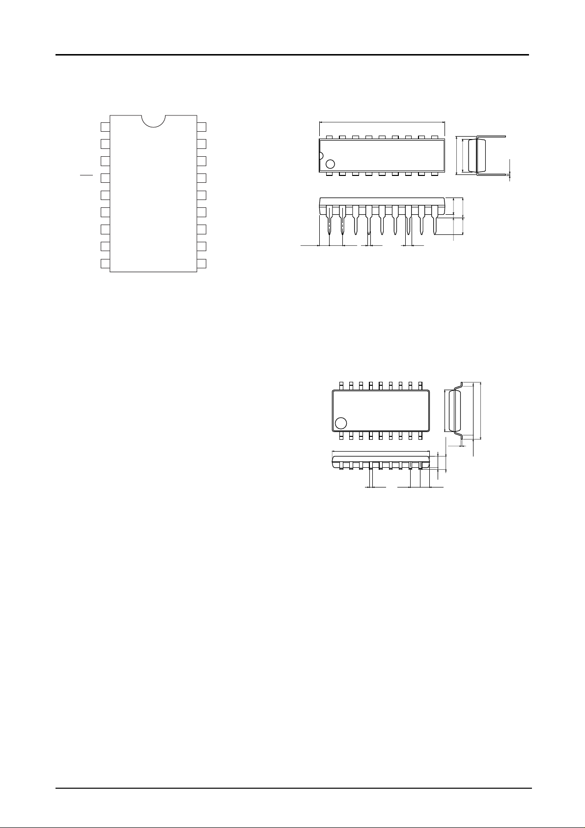
LC6527N/F/L, 6528N/F/L
Pin Assignment Package Dimentions
LC6527N / F / L unit : mm
LC6528N / F / L 3007B
OSC1
TEST
V
SS
RES
PA0
PA1
PA2
PA3
V
DD
1
2
3
4
5
6
7
8
9
Common to DIP • MFP
18
17
16
15
14
13
12
11
10
ILC00139
OSC2 / PH0
PD3
PD2
PD1
PD0
PC3
PC2
PC1
PC0
(1.84)
18
1
2.54
24.0
10
6.4
7.62
9
(3.25)
3.85max
3.3
1.20.5
0.51min
SANYO : DIP18(300mil)
0.25
• Do not immerse the package in the solder
dip tank when mounting the MFP on the substrate.
unit : mm
3095
18
1
12.6
0.35
10
5.4
6.35
9
1.27
1.22
1.5
0.1
0.15
1.8max
0.625
SANYO : MFP-18(300mil)
7.6
(Note) The package is the reference figure without the
description of the rank. Please inquire us for the
formal package.
No.4363-3/28
Page 4
Pin Name
OSC1, OSC2 : R, C or ceramic resonator for OSC PH0 : Input / output common port H 0
RES : Reset TEST : Test
PA 0-3 : Input / output common port A 0-3
PC 0-3 : Input / output common port C 0-3
PD 0-3 : Input / output common port D 0-3
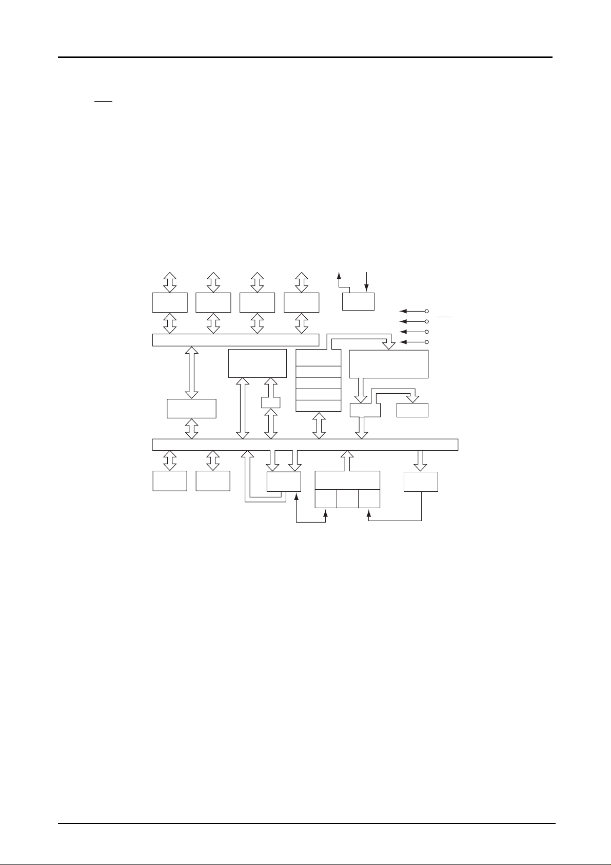
System Block Diagram
LC6527N/F/L, 6528N/F/L
LC6527N / F / L, LC6528N / F / L
PA0-3
Port A Port C Port D Port H
E A
PC0-3 PD0-3 PH0
I / O BUS
I / O Buffer
RAM
(Note 2)
DP
SYSTEM BUS
Note 1
PC
STACK1
STACK2
STACK3
STACK4
CF ZF
OSC2
STS
Note 1
OSC
OSC1
I.R
TMF
ROM
(Note 2)
I.DEC
TMALU
TEST
RES
V
DD
V
SS
ILC00140
Note1. The PH0 pin or OSC2 pin is selected by the mask option.
Note2. LC6527N / F / N ROM : 1024 bytes RAM : 64 words
LC6528N / F / N ROM : 512 bytes RAM : 32 words
No.4363-4/28
Page 5
LC6527N/F/L, 6528N/F/L
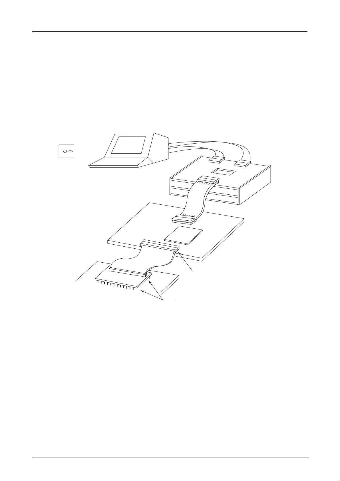
Development Support Tools
The following are available to support the program development for the LC6527, LC6528.
(1) User’s Manual
“LC6527, LC6528 User’s Manual” No. 24-6016 (’86.10.1.)
Note : Do not use “LC6523 Series User’s Manual” No.16A-7015 and No.16-9064.
(2) Development Tool Manual
For the EVA-800 or the EVA-850 system, refer to “EVA-800. LC6527, LC6528 Development Tool Manual”.
(3) Development Tools
A. For program evaluation
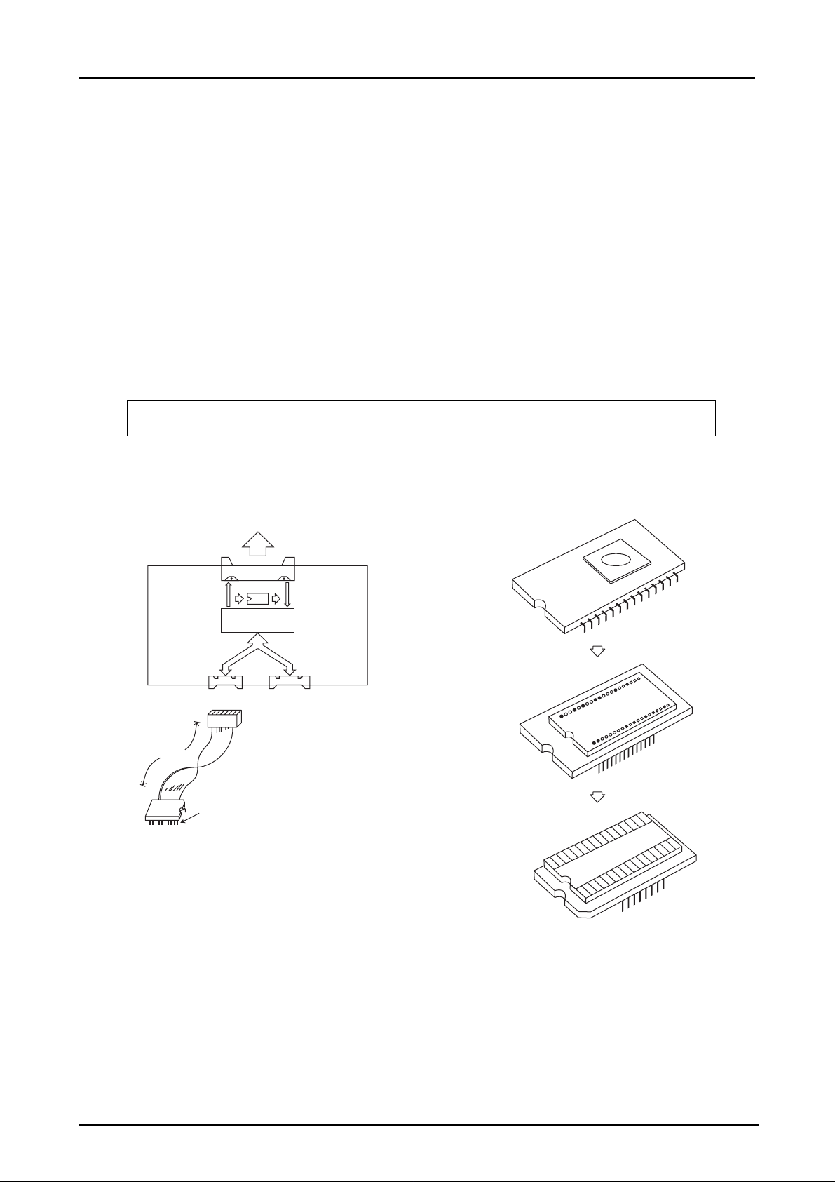
1. Piggy back (LC65PG23 / 26)
2. 23T27 ; The pin-to-pin conversion socket for the piggy back LC65PG23 / 26.
B. EVA-86000 system for program development is on development.
C. For program evaluation
microcontroller built-in EPROM (LC65E29)+conversion substrate (29T027)
Note. For notes for program evaluation, do not fail to refer to ‘4-3. Notes when evaluating programs’in
“LC6527, LC6528 User’s Manual”.
to EVA-410 or EVA-420
CN-1
EPROM
LC6596
FAP-20-03#2
CN-3
FAS-20-03B
45cm
FGP-20-01#2 removed the10 pin and 11 pin can be
used for the DIP18.
2.54mm pitch
flat cable
1 pin
2.54mm pitch
DIP18
FAP-40-03#2
NFP-30A-0112
(34A)
CN2
EPROM (2732, 2764)
Piggy back
LC65PG23 / 26
Conversion board
23T27
ILC00141
ILC00142
Fig.1 Evaluation kit terget board Fig. 2 Program evaluation
(EVA-TB6523C / 26C / 27C / 28C)
No.4363-5/28
Page 6
LC6527N/F/L, 6528N/F/L
D. For program development (EVA-800 or EVA-850 system)
1. MS-DOS for host system (Note 1)
2. Cross assembler......MS-DOS base cross assembler : <LC65S.EXE>
3. Host control program
4. Evaluation chip : LC6596
5. Emulator : EVA-800 or EVA-850 emulator and evaluation boards EVA800-TB6527 / 28
Appearance of Development Support System
• Host processor control program
• LC65S.EXE cross assembler
MS--DOS personal computer
EVA-800 or EVA-850
emulator (note 2)
CN1, CN2
LC6596
Evaluation chip board
CN3
CABLE9
FS-20
SAP20
1 pin
User's application board
Remove the 10 and 11 pin, and use for DIP18
EVA800-TB6527 / 28
ILC00143
(Note 1) MS-DOS : Trademark of Microsoft Corporation
(Note 2) The EVA-800, EVA-850 are general term for emulator. A suffix (A, B,...) is added at the end of EVA-800 and
EVA-850 as they are improved to be a newer version. Do not use the EVA-800 and EVA-850 with no suffix
added.
No.4363-6/28
Page 7

LC6527N/F/L, 6528N/F/L
Pin Description
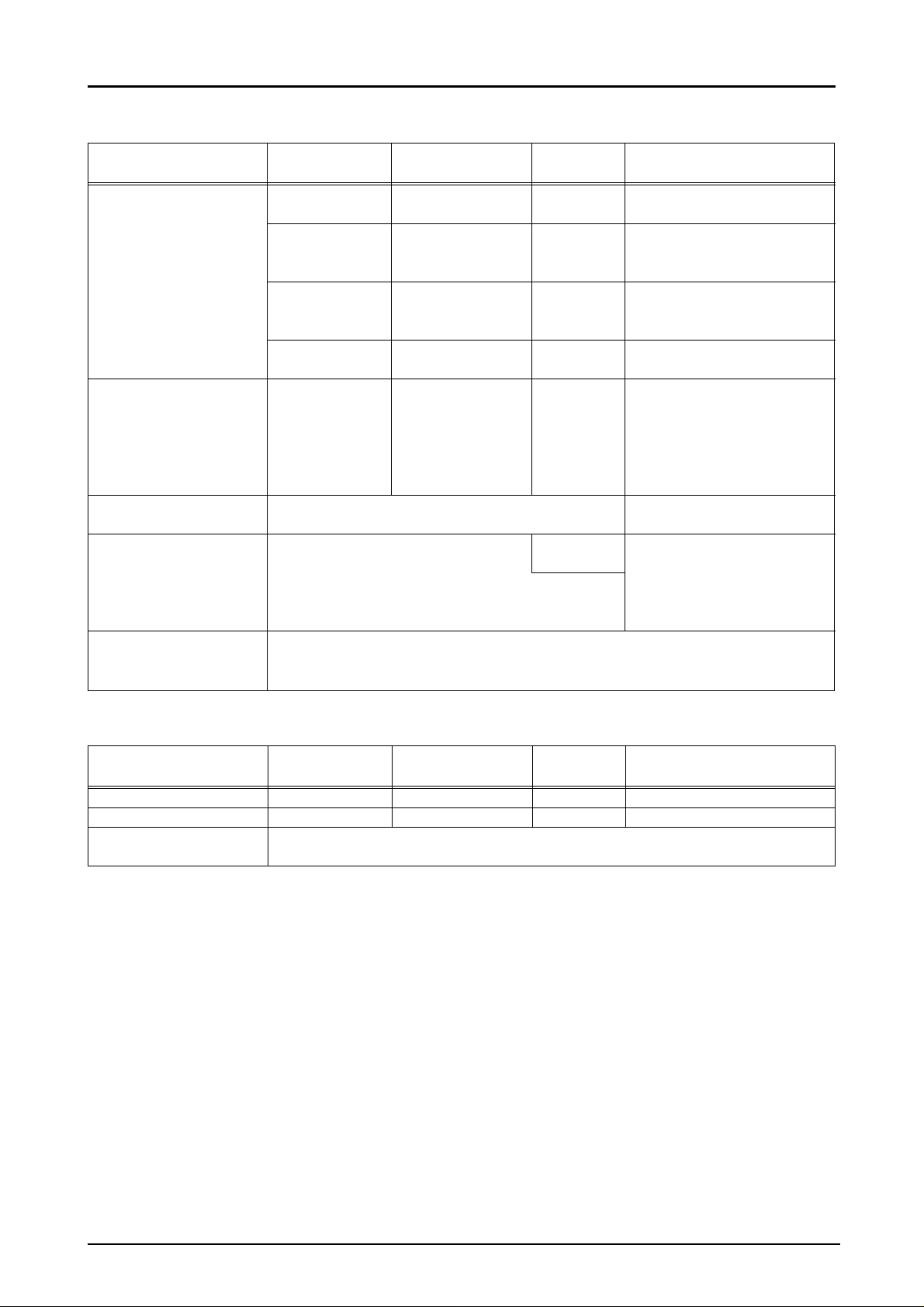
Pin name Pins I / O Function Option Reset Mode
V
DD
V
SS
OSC1 1 Input • Pin for externally connecting RC, 1) 1-pin external clock input –
PA 0 to 4 Input / • I / O port A0 to 3 1) Open drain type output • “H” output (Output
PA3 output 4-bit input (IP instruction) 2) With pull-up resistor Nch transistor : OFF)
PC0 to 4 Input / • I / O port C0 to 3 1) Open drain type output • “H” output
PC3 output same as for PA0 to 3 (Note) • “L” output
PD0 to 4 Input / • I / O port D0 to 3 Same as for PC0 to 3 Same as for PC0 to 3
PD3 output Same as for PC0 to 3
PH0 / 1 Input / • I / O port H0 Same as for PA0 to 3 Same as for PA0 to 3
OSC2 output Same as for PA0 to 3 (Note)
RES 1 Input • System reset input
TEST 1 Input • LSI test pin
1 – Power supply – –
1–
ceramic resonator for system 2) 2-pin RC OSC
clock generation. 3) 2-pin ceramic resonator
• For 1-pin external clock input, OSC
the PH0 / OSC2 pin is used as 4) Predivider option
I / O port PH0. 1. No predivider
• For 2-pin RC OSC, 2-pin ceramic 2. 1 / 3 predivider
resonator OSC, the PH0 / OSC2 3. 1 / 4 predivider
pin is used as OSC pin OSC2.
4-bit output (OP instruction) 1), 2) : Specified bit by bit
Single-bit decision (BP, BNP
instruction)
Single-bit set / reset (SPB, RPB
instruction)
• Standby is controlled by PA3.
• The PA3 pin must be free from
chattering during the HALT
instruction execution cycle.
• Option permits output at the reset 2) With pull-up resistor (Option-selectable)
mode to be “H” or “L”. 3) Output at reset mode : “H”
(Note) No standby control function 4) Output at reset mode : “L”
is provided. • 1), 2) : Specified bit by bit
• 3), 4) : Specified in a
group of 4 bits
• Single-bit configuration
• For 2-pin OSC, this pin is used as
the OSC2 pin, providing no
function as I / O port.
(Note) No standby control function
is provided
• For power-up reset, C is connected
externally.
• For reset restart, “L” level is
applied for 4 clock cycles or more.
Normally connected to V
SS
No.4363-7/28
Page 8

LC6527N/F/L, 6528N/F/L
Oscillator circuit option
Option Name Circuit Conditions, etc.
1. External clock The PH0 / OSC2 pin is used as port
2. 2-pin RC OSC The PH0 / OSC2 pin is used as OSC
Cext
OSC1
OSC1
PH0 / OSC2
PH0.
ILC00102
pin OSC2, providing no function
as port.
Rext
3. Ceramic resonator The PH0 / OSC2 pin is used as OSC
C1
OSC1
ILC00144
OSC pin OSC2, providing no function
Ceramic
resonator
C2
PH0 / OSC2
R
ILC00145
as port.
Predivider Option
Option Name Circuit Conditions, etc.
1. No predivider • Applicable to all of 3 OSC options.
(1 / 1) • The OSC frequency, external clock do not
fOSC
OSC circuit
Timing
ILC00105
2. 1 / 3 predivider • Applicable to only 2 OSC options of
fOSC
OSC circuit
1 / 3
predivider
fOSC
3
Timing
exceed 1444kHz. (LC6527N, 6528N)
• The OSC frequency, external clock do not
generator
exceed 4330kHz. (LC6527F, 6528F)
• The OSC frequency, external clock do not
exceed 1040kHz. (LC6527L, 6528L)
external clock, ceramic resonator OSC.
• The OSC frequency, external clock do not
exceed 4330kHz.
generator
ILC00106
3. 1 / 4 predivider • Applicable to only 2 OSC options of
fOSC
OSC circuit
1 / 4
predivider
fOSC
4
Timing
ILC00107
external clock, ceramic resonator OSC.
• The OSC frequency, external clock do not
exceed 4330kHz.
generator
Note : The OSC option and predivider option are summarized below. Full care must be exercised.
No.4363-8/28
Page 9
LC6527N/F/L, 6528N/F/L
Table of OSC, predivider Option of LC6527N / 28N, 27F / 28F and 27L / 28L
LC6527N, LC6528N
Circuit Configuration Frequency Predivider Option VDD Range
(Cycle time)
Ceramic resonator OSC 400kHz 1 / 1 (10µs) 3 to 6V Unusable with 1 / 3, 1 / 4
predivider
800kHz 1 / 1 (5µs) 4 to 6V
1 / 3 (15µs) 4 to 6V
1 / 4 (20µs) 4 to 6V
1MHz 1 / 1 (4µs) 4 to 6V
1 / 3 (12µs) 4 to 6V
1 / 4 (16µs) 4 to 6V
4kHz 1 / 3 (3µs) 4 to 6V Unusable with 1 / 1 predivider
1 / 4 (4µs) 4 to 6V
1-pin external clock 200k to 677kHz 1 / 1 (20 to 6µs) 3 to 6V
600k to 2000kHz 1 / 3 (20 to 6µs) 3 to 6V
800k to 2667kHz 1 / 4 (20 to 6µs) 3 to 6V
200k to 1444kHz 1 / 1 (20 to 2.77µs) 4 to 6V
600k to 4330kHz 1 / 3 (20 to 2.77µs) 4 to 6V
800k to 4330kHz 1 / 4 (20 to 3.70µs) 4 to 6V
External clock by 2-pin Same as above
RC OSC circuit
2-pin RC Used with 1 / 1 predivider, 3 to 6V
recommended constants. If used with 4 to 6V
other than recommended constants, the frequency,
predivider option, VDD range must be the same as for
1-pin external clock.
External clock input to the The ceramic oscillation circuit cannot be driven by external clock.
ceramic oscillation circuit To drive the circuit with external clock, select the external clock option or the 2-pin
RC option.
Remarks
LC6527F, LC6528F
Circuit Configuration Frequency Predivider Option VDD Range
(Cycle time)
Ceramic resonator OSC 4MHz 1 / 1 (1µs) 4.5 to 6V
1-pin external clock 200k to 4330kHz 1 / 1 (20 to 0.92µs) 4.5 to 6V
External clock input to the The ceramic oscillation circuit cannot be driven by external clock.
ceramic oscillation circuit To drive the circuit with external clock, select the external clock option.
Remarks
No.4363-9/28
Page 10

LC6527N/F/L, 6528N/F/L
LC6527L, LC6528L
Circuit Configuration Frequency Predivider Option VDD Range
(Cycle time)
Ceramic resonator OSC 400kHz 1 / 1 (10µs) 2.2 to 6V Unusable with 1 / 3, 1 / 4
predivider
800kHz 1 / 1 (5µs) 2.2 to 6V
1 / 3 (15µs) 2.2 to 6V
1 / 4 (20µs) 2.2 to 6V
1MHz 1 / 1 (4µs) 2.2 to 6V
1 / 3 (12µs) 2.2 to 6V
1 / 4 (16µs) 2.2 to 6V
4kHz 1 / 4 (4µs) 2.2 to 6V Unusable with 1 / 1, 1 / 3
predivider
1-pin external clock 200k to 1040kHz 1 / 1 (20 to 3.84µs) 2.2 to 6V
600k to 3120kHz 1 / 3 (20 to 3.84µs) 2.2 to 6V
800k to 4160kHz 1 / 4 (20 to 3.84µs) 2.2 to 6V
External clock by 2-pin Same as above
RC OSC circuit
2-pin RC Used with 1 / 1 predivider, 2.2 to 6V
recommended constants. If used with other than
recommended constants, the frequency, predivider
option, VDD range must be the same as for 1-pin
external clock.
External clock input to the The ceramic oscillation circuit cannot be driven by external clock.
ceramic oscillation circuit To drive the circuit with external clock, select the external clock option or the 2-pin
RC option.
Remarks
Option of ports C, D Output Level at the Reset Mode
For input / output common ports C, D either of the following two output levels may be selected in a group of 4 bits during
reset by option.
Option Name
Conditions, etc.
1. Output at the reset mode : “H”level All of 4 bits of ports C, D
2. Output at the reset mode : “L”level All of 4 bits of ports C, D
Option of port Output Configuration
For each input / output common port, either of the following two output configurations may be selected by option.
Option Name Circuit Conditions, etc.
1. Open drain output • Unapplicable to port PH0 / OSC2
when 2-pin RC OSC or ceramic
resonator OSC is selected.
ILC00236
2. Output with pull-up
resistor
ILC00237
No.4363-10/28
Page 11

LC6527N/F/L, 6528N/F/L
LC6527N, LC6528N
1. Absolute Maximum Ratings at Ta=25°C, VSS=0V
Parameter Symbol Pins Conditions Limits unit
Maximum VDD max V
supply voltage
Output voltage V
Input voltage VI(1) OSC1 (*1) -0.3 to VDD+0.3 V
Input / VIO(1) Port of OD type -0.3 to +15 V
output voltage VIO(2) Port of PU type -0.3 to VDD+0.3 V
Peak output I
current
Average output I
current 100ms
Allowable power
dissipation
Operating Topg
temperature
Storage Tstg
temperature
*······Under development. Do not immerse the package in the solder dip tank when mounting the MFP on the substrate.
O
VI(2) TEST, RES -0.3 to VDD+0.3 V
OP
OA
∑IOA(1)
∑IOA(2) PC0 to 3 PH0 Total current of PC0 to 3, -14 to +90 mA
Pd max(1)
Pd max(2)
DD
OSC2 Allowable up to voltage V
I / O port -2 to +20 mA
I / O port Per pin over the period of -2 to +20 mA
PA0 to 3
PD0 to 3 PD0 to 3 PH0 (*2)
Total current of PA0 to 3, -6 to +40 mA
(*2)
Ta=-40 to +85°C
(DIP package)
Ta=-40 to +85°C
(MFP package)*
-0.3 to +7.0V V
generated
300 mW
200 mW
-40 to +85
-55 to +125
°C
°C
2. Allowable Operating Conditions at Ta=-40°C to +85°C, VSS= 0V, VDD=3.0 to 6.0V
Parameter Symbol Pins Conditions
Operating V
supply voltage
Standby VST V
supply voltage (*3)
“H”-level input VIH(1) Port of OD type Output Nch Tr. OFF 0.7V
voltage (except H0)
“L”-level input VIL(1) Port Output Nch Tr. OFF
voltage VIL(2) Port Output Nch Tr. OFF
DD
VIH(2) Port of PU type Output Nch Tr. OFF 0.7V
VIH(3) H0 of OD type Output Nch Tr. OFF 0.8V
VIH(4) H0 of PU type Output Nch Tr. OFF 0.8V
VIH(5) RES 0.8V
VIH(6) OSC1 External clock mode 0.8V
VIL(3) OSC1 External clock mode
VIL(4) OSC1 External clock mode
VIL(5) TEST
VIL(6) TEST
VIL(7) RES
VIL(8) RES
V
DD
DD
(except H0)
RAM, register hold 1.8 6.0 V
VDD [V] min typ max
3.0 6.0 V
DD +13.5 V
DD
DD
DD
DD
DD
VDD=4 to 6
VDD=3 to 6
VDD=4 to 6
VDD=3 to 6
VDD=4 to 6
VDD=3 to 6
VDD=4 to 6
VDD=3 to 6
V
SS
V
SS
V
SS
V
SS
V
SS
V
SS
V
SS
V
SS
Ratings
V
DD V
+13.5
V
DD V
V
DD V
V
DD V
0.3V
0.25V
0.25V
0.2V
0.3V
0.25V
0.25V
0.2V
unit
V
DD V
DD V
DD V
DD V
DD V
DD V
DD V
DD V
No.4363-11/28
Page 12

LC6527N/F/L, 6528N/F/L
Parameter Symbol Pins Conditions
Operating fop When the 1 / 3 or
frequency (Tcyc) 1 / 4 predivider (20) (2.77) (µs)
(cycle time) option is selected, 200 667 kHz
clock must not (20) (6.0) (µs)
exceed 4.33MHz.
External clock
conditions Fig.1.
Frequency text OSC1 When clock exceeds
1.444MHz, the 1 / 3
Pulse width textH, textL OSC1 or 1 / 4 predivider
option is selected.
Rise / Fall time textR, textF OSC1
Oscillation guaranty constants
2-pin RC Cext OSC1, OSC2 Fig.2
oscillation Cext OSC1, OSC2 Fig.2
Rext OSC1, OSC2 Fig.2
Rext OSC1, OSC2 Fig.2
Ceramic Fig.3 Table 1
resonator OSC
VDD [V] min typ max
VDD=4 to 6
VDD=4 to 6
3 to 6
VDD=4 to 6
3 to 6
VDD=4 to 6
3 to 6
VDD=3 to 6
VDD=4 to 6
VDD=3 to 6
VDD=4 to 6
200 1444 kHz
200 4330 kHz
200 2667 kHz
69 ns
180 ns
Ratings
50 ns
100 ns
220±5% pF
220±5% pF
12±1% kΩ
4.7±1% kΩ
unit
3. Electrical Characteristics at Ta=-40°C to +85°C, VSS= 0V, VDD=3.0V to 6.0V
Parameter Symbol Pins Conditions
“H”-level input IIH(1) Port of OD type Output Nch Tr. OFF +5.0 µA
current (including OFF leak current
of Nch Tr.)
VIN=±13.5V
IIH(2) OSC1 External clock mode, +1.0 µA
VIN=V
“L”-level input IIL(1) Port of OD type Output Nch Tr. OFF -1.0 µA
current VIN=V
IIL(2) Port of PU type Output Nch Tr. OFF -1.3 -0.35 mA
VIN=V
IIL(3) RES VIN=V
IIL(4) OSC1 External clock mode, -1.0 µA
VIN=V
“H”-level output VOH(1) Port of PU type IOH=-50µA V
voltage VDD=4.0V to 6.0V
VOH(2) Port of PU type IOH=-10µA V
“L”-level output VOL(1) Port
voltage VOL(2) Port IOL=1.8mA, IOL of each port : 0.4 V
Hysteresis VHIS
voltage
RES, OSC1 of
schmitt type(*4)
IOL=10mA VDD=4.0V to 6.0V
1mA or less
DD
SS
SS
SS
SS
min typ max
-45 -10 µA
DD
DD
Ratings
-1.2 V
-0.5 V
1.5 V
0.1V
DD
unit
V
No.4363-12/28
Page 13

LC6527N/F/L, 6528N/F/L
Parameter Symbol Pins Conditions
Current Output Nch Tr. OFF at
dissipation operating, Port=V
2-pin RC
oscillation IDDOP(1) V
IDDOP(2) V
Ceramic IDDOP(3) V
resonator VDD=4 to 6V
oscillation IDDOP(4) V
IDDOP(5) V
IDDOP(6) V
External clock IDDOP(7) V
IDDOP(8) V
Standby mode IDDst V
Oscillation
characteristics
Ceramic OSC
Frequency fCFOSC OSC1, OSC2 Fig.3 fo=400kHz 384 400 416 kHz
(*5) OSC1, OSC2
Stable time tCFS Fig.4 fo=400kHz 10 ms
2-pin RC fMOSC OSC1, OSC2 Fig.2 Cext=220pF±5% 646 850 1117 kHz
oscillation Fig.2 Rext=4.7kΩ±1%
Frequency VDD=4 to 6V
DD
DD
DD
DD
DD
DD
DD
DD
DD
V
DD
OSC1, OSC2 Fig.3 fo=1MHz, VDD=4 to 6V 960 1000 1040 kHz
OSC1, OSC2
OSC1, OSC2 Fig.2 Cext=220pF±5% 304 400 580 kHz
Fig.2 fosc=850kHz (TYP) 1.5 4 mA
Fig.2 fosc=400kHz (TYP) 1.0 4 mA
Fig.3 4MHz, 1 / 3 predivider 2.0 5 mA
Fig.3 4MHz, 1 / 4 predivider 2.0 4 mA
Fig.3 400kHz 0.5 2 mA
Fig.3 800kHz VDD=4 to 6V 1.5 4 mA
200kHz to 667kHz, 1.5 4 mA
1 / 1 predivider
600kHz to 2000kHz,
1 / 3 predivider
800kHz to 2667kHz,
1 / 4 predivider
200kHz to 1444kHz, 2.0 5 mA
1 / 1 predivider
600kHz to 4330kHz,
1 / 3 predivider
800kHz to 4330kHz,
1 / 4 predivider VDD=4 to 6V
Output Nch Tr. OFF VDD=6V 0.05 10 µA
Port=V
DD
Fig.3 fo=800kHz, VDD=4 to 6V
Fig.3 fo=4MHz, 1 / 3 predivider
1 / 4 predivider, VDD=4 to 6V
Fig.4 fo=800kHz, 1MHz, 4MHz,
1 / 3 predivider, 1 / 4 predivider
Fig.2 Rext=12kΩ±1%
DD
VDD=4 to 6V
VDD=4 to 6V
VDD=3V 0.025 5 µA
VDD=4 to 6V
VDD=3 to 6V
min typ max
768 800 832 kHz
3840 4000 4160 kHz
Ratings
10 ms
unit
No.4363-13/28
Page 14

LC6527N/F/L, 6528N/F/L
Parameter Symbol Pins Conditions
Pull-up
resistance
I / O port pull-up RPP Port of PU type VDD=5V 14 kΩ
resistance
External reset
characteristics
Reset time tRST See Fig.5
Pin capacitance Cp f=1MHz Other than pins
to be tested, VIN=V
(*1) When oscillated internally under the oscillating conditions in Fig.3, up to the oscillation amplitude generated is
allowable.
(*2) Average over the period of 100ms.
(*3) Operating supply voltage VDD must be held until the standby mode is entered after the execution of the HALT
instruction. The PA3 pin must be free from chattering during the HALT instruction execution cycle.
(*4) The OSC1 pin can be schmitt-triggered when the 2-pin RC oscillation option or external clock oscillation option
has been selected.
(*5) fCFOSC : oscillation frequency. There is a tolerance of approximately 1% between the center frequency at the
ceramic resonator mode and the nominal value presented by the ceramic resonator supplier. For details, refer to the
specification for the ceramic resonator.
SS
min typ max
Ratings
10 pF
unit
No.4363-14/28
Page 15

LC6527N/F/L, 6528N/F/L
textF
OSC1
External clock
textL
textR
text
Fig. 1 External Clock Input Waveform
textH
(OSC2)
OPEN
V
DD
0.8V
DD
0.2VDD(VDD=3-4V)
0.25VDD(VDD=4-6V)
V
SS
ILC00146
*External clock can be used at selecting 2-pin RC option or 1-pin external clock option, and cannot be used at ceramic
resonator oscillation.
OSC1 OSC2
Rext
Cext
Fig. 2 2-pin RC Oscillation Circuit
V
DD
OSC
Unstabilized
OSC period
tCFS
OSC1 OSC2
Ceramic
C1
resonator
C2
Fig. 3 Ceramic Resonator Oscillation Circuit
Lower limit of
operating V
0V
Stabilized OSC
DD
ILC00147ILC00088
Fig. 4 Oscillation Stabilizing Period
ILC00148
No.4363-15/28
Page 16

LC6527N/F/L, 6528N/F/L
Table 1 Constants Guaranteed for
Ceramic Resonator OSC
4MHz (Murata) C1 33pF±10%
CSA4.00MG C2 33pF±10%
CST4.00MGW (built-in C) R 0Ω
4MHz (Kyocera) C1 33pF±10%
KBR4.0MSA C2 33pF±10%
KBR4.0MKS (built-in C) R 0Ω
1MHz (Murata) C1 100pF±10%
CSB1000J C2 100pF±10%
R 2.2Ω
1MHz (Kyocera) C1 100pF±10%
KBR1000F C2 100pF±10%
R0Ω
800kHz (Murata) C1 100pF±10%
CSB800J C2 100pF±10%
R 2.2Ω
800kHz (Kyocera) C1 100pF±10%
KBR800F C2 100pF±10%
R0Ω
400kHz (Murata) C1 220pF±10%
CSB400P C2 220pF±10%
R 2.2Ω
400kHz (Kyocera) C1 330pF±10%
KBR400BK C2 330pF±10%
R0Ω
RES
C
(=0.1µF)
RES
Fig. 5 Reset Circuit
(Note) When the rise time of the power supply is 0,
the reset time becomes 10ms to 100ms at
C
=0.1µF. If the rise time of the power supply
RES
is long, the value of C
so that the reset time becomes 10ms or more.
must be increased
RES
ILC00240
No.4363-16/28
Page 17

LC6527N/F/L, 6528N/F/L
RC Oscillation Characteristics of the LC6527N, LC6528N
Fig. 6 shows the RC oscillation characteristics of the LC6527N, LC6528N. For the variation range of RC OSC
frequency of the LC6527N, LC6528N, the following are guaranteed at the external constants only shown below.
1) VDD=3.0V to 6.0V, Ta=-40°C to +85°C
External constants Cext=220pF
Rext=12kΩ
304kHz≤fMOSC≤580kHz
2) VDD=4.0V to 6.0V, Ta=-40°C to +85°C
Cext=220pF
Rext=4.7kΩ
646kHz≤fMOSC≤1117kHz
If any other constants than specified above are used, the range of Rext=3kΩ to 20kΩ,
Cext=150pF to 390pF must be observed. (See Fig.6.)
(*6) : The oscillation frequency at VDD=5.0V, Ta=+25°C must be in the range of 350kHz to 750kHz.
(*7) : The oscillation frequency at VDD=4.0V to 6.0V, Ta=-40°C to +85°C and VDD=3.0V to 6.0V,
Ta=-40°C to 85°C must be within the operation clock frequency range.
f MOSC-Rext
1.5
These characteristic curves are
1000
9
8
7
6
5
4
3
f MOSC[kHz]
2
C=270pF
C=390pF
given for reference only without
guarantee.
C=150pF
VDD=5(V)
Ta=25(°C)
100
2345 2345
10 100
Rext [kΩ]
Fig. 6 RC Oscillation Frequency Data (Typ.)
ILC00149
No.4363-17/28
Page 18

LC6527N/F/L, 6528N/F/L
LC6527F, LC6528F
1. Absolute Maximum Ratings at Ta=25°C, VSS=0V
Parameter Symbol Pins Conditions Limits unit
Maximum VDD max V
supply voltage
Output voltage V
Input voltage VI(1) OSC1 (*1) -0.3 to VDD+0.3 V
Output voltage VIO(1) Port of OD type -0.3 to +15 V
Peak output I
current
Average output I
current 100ms
Allowable power
dissipation
Operating Topg
temperature
Storage Tstg
temperature
*······Under development. Do not immerse the package in the solder dip tank when mounting the MFP on the substrate.
O
VI(2) TEST, RES -0.3 to VDD+0.3 V
VIO(2) Port of PU type -0.3 to VDD+0.3 V
OP
OA
∑IOA(1)
∑IOA(2) PC0 to 3 PH0 Total current of PC0 to 3, -14 to +90 mA
Pd max(1)
Pd max(2)
DD
OSC2 Allowable up to voltage V
I / O port -2 to +20 mA
I / O port Per pin over the period of -2 to +20 mA
PA0 to 3
PD0 to 3 PD0 to 3, PH0 (*2)
Total current of PA0 to 3, -6 to +40 mA
(*2)
Ta=-40 to +85°C
(DIP package)
Ta=-40 to +85°C
(MFP package)*
-0.3 to +7.0V V
ganerated
300 mW
200 mW
-40 to +85
-55 to +125
°C
°C
2. Allowable Operating Conditions at Ta=-40°C to +85°C, VSS= 0V, VDD=4.5 to 6.0V
Parameter Symbol Pins Conditions
Operating V
supply voltage
Standby VST V
supply voltage
“H”-level input VIH(1) Port of OD type Output Nch Tr. OFF 0.7V
voltage (except H0)
“L”-level input VIL(1) Port Output Nch Tr. OFF V
voltage VIL(2) OSC1 External clock mode V
DD
VIH(2) Port of PU type Output Nch Tr. OFF 0.7V
VIH(3) H0 of OD type Output Nch Tr. OFF 0.8V
VIH(4) H0 of PU type Output Nch Tr. OFF 0.8V
VIH(5) RES 0.8V
VIH(6) OSC1 External clock mode 0.8V
VIL(3) TEST V
VIL(4) RES V
V
DD
DD
(except H0)
RAM, register hold (*3) 1.8 6.0 V
min typ max
4.5 6.0 V
DD
DD
DD
DD
DD
DD
SS
SS
SS
SS
Ratings
+13.5
V
DD V
+13.5
V
DD V
V
DD V
V
DD V
0.3V
0.25V
0.3V
0.25V
unit
V
V
DD V
DD V
DD V
DD V
No.4363-18/28
Page 19

LC6527N/F/L, 6528N/F/L
Parameter Symbol Pins Conditions
Operating fop 200 4330 kHz
frequency (Tcyc) (20) (0.92) (µs)
(Cycle time)
External clock
conditions
Frequency text OSC1 200 4330 kHz
Pulse width textH, textL OSC1 Fig.1 69 ns
Rise / Fall time textR, textF OSC1 50 ns
Oscillation guaranteed constants
ceramic Fig.2 See Table 1
resonator OSC
3. Electrical Characteristics at Ta=-40°C to +85°C, VSS= 0V, VDD=4.5V to 6.0V
Parameter Symbol Pins Conditions
“H”-level input IIH(1) Port of OD type Output Nch Tr. OFF +5.0 µA
current (including OFF leak current
of Nch Tr.)
VIN=±13.5V
IIH(2) OSC1 External clock mode, +1.0 µA
VIN=V
DD
“L”-level input IIL(1) Port of OD type Output Nch Tr. OFF -1.0 µA
current VIN=V
IIL(2) Port of PU type Output Nch Tr. OFF -1.3 -0.35 mA
IIL(3) RES VIN=V
IIL(4) OSC1 External clock mode, -1.0 µA
“H”-level output VOH(1) Port of PU type IOH=-50µA V
voltage VOH(2) Port of PU type IOH=-10µA V
“L”-level output VOL(1) Port
voltage VOL(2) Port IOL=1.8mA, IOL of each port : 0.4 V
Hysteresis VHIS
voltage
RES, OSC1 of
schmitt type(*4)
SS
VIN=V
SS
SS
VIN=V
SS
IOL=10mA
1mA or less
min typ max
min typ max
-45 -10 µA
DD
DD
Ratings
Ratings
-1.2 V
-0.5 V
1.5 V
0.1V
DD
unit
unit
V
No.4363-19/28
Page 20

LC6527N/F/L, 6528N/F/L
Parameter Symbol Pins Conditions
Current
dissipation
Ceramic IDDOP(1) V
resonator OSC *1
External clock IDDOP(2) V
Standby mode IDDst V
Oscillation
characteristics
Ceramic OSC
Frequency fCFOSC OSC1, OSC2 Fig.2 fo=4MHz (*5) 3840 4000 4160 kHz
Stable time tCFS Fig.3 fo=4MHz 10 ms
Pull-up
resistance
I / O port pull-up RPP Port of PU type VDD=5V 14 kΩ
resistance
External reset
characteristics
Reset time tRST See Fig.4
Pin capacitance Cp f=1MHz, other than pins 10 pF
DD
DD
DD
V
DD
Fig.2 4MHz 1.5 3.5 mA
200kHz to 4330kHz 1.5 3.5 mA
*1 Output Nch Tr.OFF at
Operating mode
Port=V
Output Nch Tr. OFF VDD=6V 0.05 10 µA
Port=V
to be tested, VIN=V
DD
VDD=3V 0.025 5 µA
SS
min typ max
DD
Ratings
unit
(*1) When oscillated internally under the oscillating conditions in Fig.2, up to the oscillation amplitude generated is
allowable.
(*2) Average over the period of 100ms.
(*3) Operating supply voltage VDD must be held until the standby mode is entered after the execution of the HALT
instruction. The PA3 pin must be free from chattering during the HALT instruction execution cycle.
(*4) The OSC1 pin can be schmitt-triggered when the external clock oscillation option has been selected.
(*5) fCFOSC : Oscillatable frequency.
No.4363-20/28
Page 21

LC6527N/F/L, 6528N/F/L
textF
(OSC2)
OPEN
textH
textL
OSC1
External clock
textR
text
Fig. 1 External Clock Input Waveform
V
DD
0.8V
DD
0.25V
DD
V
SS
ILC00150
V
DD
Lower limit of
operating V
DD
OSC1 OSC2
OSC
Ceramic
C1
Fig. 2 Ceramic Resonator OSC Circuit Fig. 3 OSC Stabilizing Period
resonator
C2
ILC00151
Unstabilized
OSC period
tCFS
Table 1 Constants Guaranteed for
Ceramic Resonator OSC
4MHz (Murarta) C1 33pF±10%
CSA4.00MG C2 33pF±10%
RES
CST4.00MGW (built-in C) R 0Ω
4MHz (Kyocera) C1 33pF±10%
C
RES
KBR4.0MSA C2 33pF±10%
KBR4.0MKS (built-in C) R 0Ω
Fig. 4 Reset Circuit
0V
Stabilized OSC
ILC00152
(=0.1µF)
ILC00153
(Note) When the rise time of the power supply is 0,
the reset time becomes 10ms to 100ms at
C
=0.1µF. If the rise time of the power
RES
supply is long, the value of C
RES
must be
increased so that the reset time becomes
10ms or more.
No.4363-21/28
Page 22

LC6527N/F/L, 6528N/F/L
LC6527L, LC6528L
1. Absolute Maximum Ratings at Ta=25°C, VSS=0V
Parameter Symbol Pins Conditions Limits unit
Maximum VDD max V
supply voltage
Output voltage V
Input voltage VI(1) OSC1 (*1) -0.3 to VDD+0.3 V
Input / VIO(1) Port of OD type -0.3 to +15 V
output voltage VIO(2) Port of PU type -0.3 to VDD+0.3 V
Peak output I
current
Average output I
current 100ms
Allowable power
dissipation
Operating Topg
temperature
Storage Tstg
temperature
*······Under development. Do not immerse the package in the solder dip tank when mounting the MFP on the substrate.
O
VI(2) TEST, RES -0.3 to VDD+0.3 V
OP
OA
∑IOA(1)
∑IOA(2) PC0 to 3 PH0 Total current of PC0 to 3, -14 to +90 mA
Pd max(1)
Pd max(2)
DD
OSC2 Allowable up to votage V
I / O port -2 to +20 mA
I / O port Per pin over the period of -2 to +20 mA
PA0 to 3
PD0 to 3 PD0 to 3 PH0 (*2)
Total current of PA0 to 3, -6 to +40 mA
(*2)
Ta=-40 to +85°C
(DIP package)
Ta=-40 to +85°C
(MFP package)*
-0.3 to +7.0 V
ganerated
250 mW
150 mW
-40 to +85
-55 to +125
°C
°C
2. Allowable Operating Conditions at Ta=-40°C to 85°C, VSS= 0V, VDD=2.2 to 6.0V
Parameter Symbol Pins Conditions
Operating V
supply voltage
Standby VST V
supply voltage
“H”-level input VIH(1) Port of OD type Output Nch Tr. OFF 0.7V
voltage (except H0)
“L”-level input VIL(1) Port Output Nch Tr. OFF V
voltage VIL(2) OSC1 External clock V
DD
VIH(2) Port of PU type Output Nch Tr. OFF 0.7V
VIH(3) H0 of OD type Output Nch Tr. OFF 0.8V
VIH(4) H0 of PU type Output Nch Tr. OFF 0.8V
VIH(5) RES 0.8V
VIH(6) OSC1 External clock 0.8V
VIL(3) TEST V
VIL(4) RES V
V
DD
DD
(except H0)
RAM, register hold (*3) 1.8 6.0 V
min typ max
2.2 6.0 V
DD
DD
DD
DD
DD
DD
SS
SS
SS
SS
Ratings
+13.5
V
DD V
+13.5
V
DD V
V
DD V
V
DD V
0.2V
0.15V
0.2V
0.15V
unit
V
V
DD V
DD V
DD V
DD V
No.4363-22/28
Page 23

LC6527N/F/L, 6528N/F/L
Parameter Symbol Pins Conditions
Operating fop When the 1 / 3 or 1 / 4 200 1040 kHz
frequency (Tcyc) predivider option is selected, (20) (3.84) (µs)
(cycle time) clock must not exceed
4.16MHz.
External clock
conditions
Frequency text OSC1 Fig.1 When clock exceeds 200 4160 kHz
Pulse width textH, textL OSC1 1.040MHz, the 1 / 3 or 1 / 4 100 ns
Rise / fall time textR, textF OSC1 predivider option is selected. 100 ns
Oscillation guaranteed constants
2-pin RC Cext OSC1, OSC2 Fig.2 220±5% pF
oscillation Rext 12±1% kΩ
Ceramic Fig.3 See Table 1.
oscillation
3. Electrical Characteristics at Ta=-40°C to +85°C, VSS= 0V, VDD=2.2V to 6.0V
Parameter Symbol Pins Conditions
“H”-level input IIH(1) Port of OD type Output Nch Tr. OFF +5.0 µA
current (including OFF leak current
of Nch Tr.)
VIN=±13.5V
IIH(2) OSC1 External clock mode, +1.0 µA
VIN=V
DD
“L”-level input IIL(1) Port of OD type Output Nch Tr. OFF -1.0 µA
current VIN=V
IIL(2) Port of PU type Output Nch Tr. OFF -1.3 -0.35 mA
IIL(3) RES VIN=V
IIL(4) OSC1 External clock mode, -1.0 µA
“H”-level output V
voltage
“L”-level output VOL(1) Port
voltage VOL(2) Port IOL=1mA, IOL of each port : 0.4 V
Hysteresis VHIS
voltage
OH
Port of PU type IOH=-10µA V
RES, OSC1 of
schmitt type(*4)
SS
VIN=V
SS
SS
VIN=V
SS
IOL=3mA
1mA or less
min typ max
min typ max
-45 -10 µA
DD
Ratings
Ratings
-0.5 V
1.5 V
0.1V
DD
unit
unit
V
No.4363-23/28
Page 24

LC6527N/F/L, 6528N/F/L
Parameter Symbol Pins Conditions
Current Output Nch Tr. OFF at
dissipation operating, Port=V
2-pin RC OSC IDDOP(1) V
Ceramic OSC IDDOP(2) V
IDDOP(3) V
IDDOP(4) V
IDDOP(5) V
External clock IDDOP(6) V
Standby mode IDDst V
Oscillation
characteristics
Ceramic OSC
Frequency fCFOSC OSC1, OSC2 Fig.3 fo=400kHz 384 400 416 kHz
(*5) OSC1, OSC2
Stable time tCFS Fig.4 fo=400kHz 10 ms
2-pin RC OSC fMOSC OSC1, OSC2 Fig.2 Cext=220pF±5% 281 400 580 kHz
Frequency Fig.2 Rext=12kΩ±1%
Pull-up
resistance
I / O port pull-up RPP Port of PU type VDD=5V 14 kΩ
resistance
External reset
characteristics
Reset time tRST See Fig.5.
Pin capacitance Cp f=1MHz Other than pins 10 pF
DD
DD
DD
DD
DD
DD
DD
V
DD
OSC1, OSC2 Fig.3 fo=1MHz 960 1000 1040 kHz
OSC1, OSC2
Fig.2 fOSC=400kHz (TYP) 0.8 2.5 mA
Fig.3 4MHz, 1 / 4 predivider 1.2 2.5 mA
Fig.3 4MHz, 1 / 4 predivider 0.5 1 mA
Fig.3 400kHz 0.5 2 mA
Fig.3 800kHz 1.0 2.5 mA
200kHz to 667kHz, 1.0 2.5 mA
1 / 1 predivider
600kHz to 2000kHz,
1 / 3 predivider
800kHz to 2667kHz,
1 / 4 predivider
Output Nch Tr. OFF VDD=6V 0.05 10 µA
Port=V
Fig.3 fo=800kHz
Fig.3 fo=4MHz
1 / 4 predivider
Fig.4 fo=800kHz, 1MHz, 10 ms
4MHz, 1 / 4 predivider
to be tested, VIN=V
DD
DD
VDD=2.2V
VDD=2.2V 0.025 5 µA
SS
min typ max
768 800 832 kHz
3840 4000 4160 kHz
Ratings
unit
(*1) When oscillated internally under the oscillating conditions in Fig.3, up to the oscillation amplitude generated is
allowable.
(*2) Average over the period of 100ms.
(*3) Operating supply voltage VDD must be held until the standby mode is entered after the execution of the HALT
instruction. The PA3 pin must be free from chattering during the HALT instruction execution cycle.
(*4) The OSC1 pin can be schmitt-triggered when the 2-pin RC oscillation option or external clock oscillation option
has been selected.
(*5) fCFOSC : Oscillatable frequency. There is a tolerance of approximately 1% between the center frequency at the
ceramic resonator mode and the nominal value presented by the ceramic resonator supplier. For details, refer to the
specification for the ceramic resonator.
No.4363-24/28
Page 25

LC6527N/F/L, 6528N/F/L
textF
OSC1
External clock
textL
textR
text
Fig. 1 External Clock Input Waveform
(OSC2)
OPEN
textH
V
DD
0.8V
0.15V
V
SS
ILC00154
DD
DD
*External clock can be used at selecting 2-pin RC option or 1-pin external clock option, and cannot be used at ceramic
resonator oscillation.
OSC1 OSC2
Rext
Cext
Fig. 2 2-pin RC Oscillation Circuit
ILC00088
V
DD
OSC
Unstabilized
OSC period
tCFS
OSC1 OSC2
Ceramic
C1
resonator
C2
Fig. 3 Ceramic Resonator Oscillation Circuit
Lower limit of
operating V
0V
Stabilized OSC
DD
ILC00147
Fig. 4 Oscillation Stabilizing Period
ILC00148
No.4363-25/28
Page 26

LC6527N/F/L, 6528N/F/L
Table 1 Constants Guaranteed for
Ceramic Resonator OSC
4MHz (Murata) C1 33pF±10%
CSA4.00MGU C2 33pF±10%
CST4.00MGWU (built-in C)
1MHz (Murata) C1 100pF±10%
CSB1000J C2 100pF±10%
1MHz (Kyocera) C1 100pF±10%
KBR1000F C2 100pF±10%
800kHz (Murata) C1 100pF±10%
CSB800J C2 100pF±10%
800kHz (Kyocera) C1 100pF±10%
KBR800F C2 100pF±10%
400kHz (Murata) C1 220pF±10%
CSB400P C2 220pF±10%
400kHz (Kyocera) C1 330pF±10%
KBR400BK C2 330pF±10%
R0Ω
R 2.2Ω
R0Ω
R 2.2Ω
R0Ω
R 2.2Ω
R0Ω
RES
C
(=0.1µF)
RES
Fig. 5 Reset Circuit
(Note) When the rise time of the power supply is 0,
the reset time becomes 10ms to 100ms at
C
=0.1µF. If the rise time of the power supply
RES
is long, the value of C
so that the reset time becomes 10ms or more.
must be increased
RES
ILC00240
No.4363-26/28
Page 27

LC6527N/F/L, 6528N/F/L
RC Oscillation Characteristic of the LC6527L, LC6528L
Fig. 6 shows the RC oscillation characteristic of the LC6527L, 6528L. For the variation range of RC OSC frequency of
the LC6527L, 6528L, the following are guaranteed at the external constants only shown below.
VDD=2.2V to 6.0V, Ta=-40°C to +85°C
External constants Cext=220pF
Rext=12kΩ
281kHz≤fMOSC≤580kHz
If any other constants than specified above are used, the range of Rext=3kΩ to 20kΩ,
Cext=150pF to 390pF must be observed. (See Fig.6.)
(*6) : The oscillation frequency at VDD=5.0V, Ta=+25°C must be in the range of 350kHz to 500kHz.
(*7) : The oscillation frequency at VDD=2.2V to 6.0V, Ta=-40°C to +85°C must be within the operation
clock frequency range.
f MOSC-Rext
1.5
These characteristic curves are
1000
9
8
7
6
5
4
3
f MOSC[kHz]
2
C=270pF
C=390pF
given for reference only without
guarantee.
C=150pF
VDD=5(V)
Ta=25(°C)
100
2345 2345
10 100
Rext [kΩ]
Fig. 6 RC Oscillation Frequency Data (Typ.)
ILC00149
No.4363-27/28
Page 28

LC6527N/F/L, 6528N/F/L
Specifications of any and all SANYO products described or contained herein stipulate the performance,
characteristics, and functions of the described products in the independent state, and are not guarantees
of the performance, characteristics, and functions of the described products as mounted in the customer's
products or equipment. To verify symptoms and states that cannot be evaluated in an independent device,
the customer should always evaluate and test devices mounted in the customer's products or equipment.
SANYO Electric Co., Ltd. strives to supply high-quality high-reliability products. However, any and all
semiconductor products fail with some probability. It is possible that these probabilistic failures could
give rise to accidents or events that could endanger human lives, that could give rise to smoke or fire,
or that could cause damage to other property. When designing equipment, adopt safety measures so
that these kinds of accidents or events cannot occur. Such measures include but are not limited to protective
circuits and error prevention circuits for safe design, redundant design, and structural design.
In the event that any or all SANYO products(including technical data,services) described or
contained herein are controlled under any of applicable local export control laws and regulations,
such products must not be exported without obtaining the export license from the authorities
concerned in accordance with the above law.
No part of this publication may be reproduced or transmitted in any form or by any means, electronic or
mechanical, including photocopying and recording, or any information storage or retrieval system,
or otherwise, without the prior written permission of SANYO Electric Co. , Ltd.
Any and all information described or contained herein are subject to change without notice due to
product/technology improvement, etc. When designing equipment, refer to the "Delivery Specification"
for the SANYO product that you intend to use.
Information (including circuit diagrams and circuit parameters) herein is for example only ; it is not
guaranteed for volume production. SANYO believes information herein is accurate and reliable, but
no guarantees are made or implied regarding its use or any infringements of intellectual property rights
or other rights of third parties.
This catalog provides information as of January, 2001. Specifications and information herein are subject to
change without notice.
PS
No.4363-28/28
 Loading...